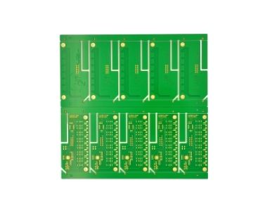
Excellent 12 Layer PCB Manufacturer from China
Excellent 12 Layer PCB Manufacturer from China
SMTFAB is a global brand in the PCB manufacturing industry. Featuring quality products made in China, we offer you the best price for the best quality 12 Layer PCB.
- Meet IPC Class 2 or 3 standard
- Professional engineering team
- Quick turn-around time, no delays
- Sales support services 24/4, on your time zone
- 100% customer satisfaction guaranteed
SMTFAB 12 Layer PCB to Fast Track Your Business
Your business depends on making the right decisions. Part of that is choosing quality products that are cost-effective.
SMTFAB has been in the PCB manufacturing industry for more than ten years. With this amount of time, we have perfected 12 Layer PCB fabrication.
Let’s accelerate your business growth. Why look for another supplier of PCBs when SMTFAB is clearly the best? We can custom make a product just for you.
Call us now for your 12 Layer PCB orders!
Types of 12 Layer PCBFor Your Specific Needs

The many uses of our 12 Layer Multilayer PCB span from digital technology to medical-related devices. Compact and lightweight, this type of PCB has increased functionality due Plated-Through Hole technology utilization.

A compound type of PCB stack-up, the 12 Layer HDI PCB can be found in satellites, 5G applications, and others. Like most advanced Multilayer PCBs, component interconnection should be done precisely.

For above 1GHz, the 12 Layer High-Frequency PCBs were developed. The demand on this PCB because of its ability to facilitate superb signal transmission. In order for this to happen, PTFE or FR-4 is the material used.

The special need for high temperature endurance necessitated the fabrication of the 12 Layer High-Tg PCB. SMTFAB can deliver this product to you by bulk, we have sufficient stock of ISOLA/Arlon material.

The Rigid 12 Layer PCB has durability and stability as main advantages. Most Rigid PCBs are used in industrial applications, like for most manufacturing machinery, telecommunication equipment, external antenna, etc.

SMTFAB’s 12 Layer Rigid-Flex PCB are folded into different types of structures inside many digital products. Rigid-Flex PCBs can be found inside smartphones and tablets since these types of devices require high-density circuit design.
SMTFAB is a Respected Supplier of 12 Layer PCBs
We’ve got a video to show you about how great SMTFAB will be for your business. After watching this, you will believe how capable we are in PCB fabrication.
Not only are we the best for 12 Layer PCB needs, we can make other types of PCBs for you. Bulk orders are not a problem for us.
You can see for yourself how professional and orderly SMTFAB workers are. We have full international certifications, so you will feel safe with our PCB products.

Related 12 Layer PCB


12 Layer PCB Production Details As Following Up
- Production Facility
- PCB Capabilities
- PCB Materials
- Shipping Methods
- Payment Methods
- Send Us Inquiry


| Item | Capability |
| Layer Count | 1-40layers |
| Base Material | KB、Shengyi、ShengyiSF305、FR408、FR408HR、IS410、FR406、GETEK、370HR、IT180A、Rogers4350B、Rogers4000、PTFE Laminates(Rogers series、Taconic series、Arlon series、Nelco series)、Rogers/Taconic/Arlon/Nelco laminate with FR-4 material(including partial Ro4350B hybrid laminating with FR-4) |
| Board Type | Backplane、HDI、High multi-layer 、blind&buried PCB、Embedded Capacitance、Embedded resistance board 、Heavy copper power PCB、Backdrill. |
| Board Thickness | 0.2-5.0mm |
| Copper Thickness | Min. 1/2 OZ, Max. 10 OZ |
| PTH Wall | 25um(1mil) |
| Maximum Board Size | 1100*500mm(43”*19”) |
| Min laser drilling size | 4mil |
| Min. Spacing/Tracing | 2.7mil/2.7mil |
| Solder Mask | Green, Black, Blue, Red, White, Yellow,Purple matte/glossy |
| Surface Treatment | Flash gold(electroplated gold)、ENIG、Hard gold、Flash gold、HASL Lead free、OSP、ENEPIG、Soft gold、Immersion silver、Immersion Tin、ENIG+OSP,ENIG+Gold finger,Flash gold(electroplated gold)+Gold finger,Immersion silver+Gold finger,Immersion Tin+Gold finger. |
| Min. Annular Ring | 3mil |
| Aspect ratio | 10:1(HASL Lead free、HASL Lead、ENIG、Immersion Tin、Immersion silver、ENEPIG);8:1(OSP) |
| Impedance control | ±5ohm(<50ohm), ±10%(≥50ohm) |
| Other Techniques | Blind/Buried Via |
| Gold Fingers | |
| Press Fit | |
| Via in Pad | |
| Electrical Test |
Here there’re many laminate material datasheets, they’re useful and helpful for you, please see them:
| SUPPLIER | PCB LAMINATE | TYPE | MATERIAL DATASHEET | TG | TD | DK(1MHZ) | DK(1GHZ) | DK(10GHZ) |
| KB | KB-6160 | FR4 | DOWNLOAD | 135 | 305 | 4.35 | – | – |
| KB-6160A | FR4 | DOWNLOAD | 135 | 305 | 4.35 | – | – | |
| KB-6160C | FR4 | DOWNLOAD | 135 | 314 | 4.7 | – | – | |
| KB-6150 KB-6150C | FR4 | DOWNLOAD | 132 | 305 | 4.6 | – | – | |
| KB-6164 | FR4 | DOWNLOAD | 142 | 330 | 4.8 | – | – | |
| KB-6164F | FR4 | DOWNLOAD | 145 | 340 | 4.8 | – | – | |
| KB-6165F | FR4 | DOWNLOAD | 150 | 346 | 4.8 | – | – | |
| KB-6167F | FR4 | DOWNLOAD | 170 | 349 | 4.8 | – | – | |
| SHENGYI | S1141 | FR4 | DOWNLOAD | 135 | 310 | 4.6 | – | – |
| S1141KF | FR4 | DOWNLOAD | 140 | 350 | 4.7 | – | – | |
| S1000 | FR4 | DOWNLOAD | 155 | 335 | 4.9 | – | – | |
| S1170 | FR4 | DOWNLOAD | 170 | 335 | 4.6 | – | – | |
| S1000-2 | FR4 | DOWNLOAD | 170 | 335 | 4.8 | – | – | |
| S1155 | FR4 | DOWNLOAD | 135 | 370 | 4.7 | – | – | |
| ITEQ | IT-158 | FR4 | DOWNLOAD | 150 | 340 | 4.6-4.8 | – | – |
| IT-180 | FR4 | DOWNLOAD | 180 | 350 | 4.5-4.7 | – | – | |
| TUC | TU-768 | FR4 | DOWNLOAD | 180 | 350 | – | 4.3-4.4 | 4.3 |
| TU-872 | Modified Epoxy | DOWNLOAD | 200 | 340 | – | 3.8-4.0 | 3.8 | |
| ROGERS | RO 3003 | Cer/PTFE | DOWNLOAD | – | 500 | – | – | 3 |
| RO 3010 | Cer/PTFE | DOWNLOAD | – | 500 | – | – | 10.2 | |
| RO 4003 | Hydrocarbon/Cer | DOWNLOAD | >280 | 425 | – | – | 3.38 | |
| RO 4350B | Hydrocarbon/Cer | DOWNLOAD | >280 | 390 | – | – | 3.48 | |
| RT/duroid 5880 | PTFE/Glass | DOWNLOAD | – | 500 | – | – | 2.2 | |
| ISOLA | Polyclad 370HR | FR4 | DOWNLOAD | 170 | 340 | 4.8-5.1 | – | – |
| FR406-HR | FR4 | DOWNLOAD | 190 | 325 | 3.91 | 3.86 | 3.81 | |
| FR408-HR | FR4 | DOWNLOAD | 200 | 360 | 3.72 | 3.69 | 3.65 | |
| P96 | Polyimide | DOWNLOAD | 260 | 416 | – | 3.78 | 3.73 | |
| Hitachi | MCL-BE- 67G | Modified Epoxy | DOWNLOAD | 140 | 340 | 4.9 | 4.4 | – |
| MCL-E-679F | FR4 | DOWNLOAD | 170 | 350 | 4.2-4.4 | 4.3-4.5 | – | |
| MCL-LX-67Y | Special Laminate | DOWNLOAD | 185-195 | 325-345 | – | 3.4-3.6 | – | |
| Nelco | N4000-13 | Modified Epoxy | DOWNLOAD | 210-240 | 365 | – | 3.7 | 3.6 |
| N4000-13EP | Modified Epoxy | DOWNLOAD | 210-240 | 350 | – | 3.4 | 3.2 | |
| N4000-13SI | Modified Epoxy | DOWNLOAD | 210-240 | 350 | – | 3.4 | 3.2 | |
| N4000-13EP SI | Modified Epoxy | DOWNLOAD | 210-240 | 350 | – | 3.4 | 3.2 | |
| Taconic | TLX-6 | PTFE | DOWNLOAD | – | – | – | – | 2.65 |
| TLX-7 | PTFE | DOWNLOAD | – | – | – | – | 2.6 | |
| TLX-8 | PTFE | DOWNLOAD | – | – | – | – | 2.55 | |
| TLX-9 | PTFE | DOWNLOAD | – | – | – | – | 2.45 | |
| RF35 | PTFE | DOWNLOAD | <315 | – | 3.5 | – | 3.5 | |
| TLC-27 | PTFE | DOWNLOAD | – | – | – | – | 2.75 | |
| TLC-30 | PTFE | DOWNLOAD | – | – | – | – | 3 | |
| TLC-32 | PTFE | DOWNLOAD | – | – | – | – | 3.2 | |
| Arlon | Arlon 25N | Cer | DOWNLOAD | 260 | – | – | – | 3.38 |
| Arlon 25FR | Cer | DOWNLOAD | 260 | – | – | – | 3.58 | |
| Arlon 33N | Polymide | DOWNLOAD | >250 | 353 | 4 | – | – | |
| Arlon 35N | Polymide | DOWNLOAD | >250 | 363 | 4.2 | – | – | |
| Arlon 85N | Polymide | DOWNLOAD | 250 | 387 | 4.2 | – | – | |
| Stablcor | ST325 | – | DOWNLOAD | Thermal conductivity:75w/m.k(with 1oz copper) | ||||
| ST10 | – | DOWNLOAD | Thermal conductivity:325w/m.k(with 1oz copper) | |||||
| Panasonic | R-1566W | FR4 | DOWNLOAD | 140 | 330 | 4.95 | 4.7 | 4.65 |
| Ventec | VT-901 | Polymide | DOWNLOAD | 250 | 390 | 4.2-4.5 | 4.0-4.3 | – |
| VT-90H | Polymide | DOWNLOAD | 250 | 390 | 4.2-4.5 | 4.0-4.3 | – | |
| Bergquist | ht-04503 | – | DOWNLOAD | Thermal conductivity:2.2w/m.k(with 1oz copper) | ||||
Delivery
SMTFAB offers flexible shipping methods for our customers, you may choose from one of the methods below.
1. DHL
DHL offers international express services in over 220 countries.
DHL partners with SMTFAB and offers very competitive rates to customers of SMTFAB.
It normally takes 3-7 business days for the package to be delivered around the world.

2. UPS
UPS gets the facts and figures about the world’s largest package delivery company and one of the leading global providers of specialized transportation and logistics services.
It normally takes 3-7 business days to deliver a package to most of the addresses in the world.

3. TNT
TNT has 56,000 employees in 61 countries.
It takes 4-9 business days to deliver the packages to the hands
of our customers.

4. FedEx
FedEx offers delivery solutions for customers around the world.
It takes 4-7 business days to deliver the packages to the hands
of our customers.

5. Air, Sea/Air, and Sea
If your order is of large volume with SMTFAB, you can also choose
to ship via air, sea/air combined, and sea when necessary.
Please contact your sales representative for shipping solutions.
Note: if you need others, please contact your sales representative for shipping solutions.
On our website you can use the following payment methods:
Telegraphic Transfer(TT): A telegraphic transfer (TT) is an electronic method of transferring funds utilized primarily for overseas wire transactions. It’s very convenient to transfer.
Bank/Wire transfer: To pay by wire transfer using your bank account, you need to visit your nearest bank branch with the wire transfer information. Your payment will be completed 3-5 business days after you have finished the money transfer.
Paypal: Pay easily, fast and secure with PayPal. many other credit and debit cards via PayPal.
Credit Card: You can pay with credit card: Visa, Visa Electron, MasterCard, Maestro.
[contact-form-7 id=”764″ title=”Quick Quote”]
Rely on SMTFAB for All Your 12 Layer PCB Requirements
Our 12 Layer PCB follows advanced manufacturing technology, with full ISO and UL certification. We use automated inspection and other testing methods such as X-ray tests and functional tests to assure you of the best quality 12 Layer PCB.
SMTFAB’s 12 Layer PCB can fully optimize your PCB projects.
- Choose from rigid, flexible, or rigid-flexible options
- Streamlined manufacturing process
- Compact and lightweight product
- Supports high wiring density
- Advanced material options (RoHS-compliant)
We have extensive knowledge and experience in manufacturing specialized PCBs. Our PCBs are used for hi-tech applications across many different industries. In fact, our facilities have the capacity to make HDI PCBs, Microvia PCBs, as well as 5G PCBs for today’s digital consumption.
Affordability is one of our selling points. As we are dedicated to making your business succeed, we give you the best-value products to boost your profit.
To make sure that you are happy with your 12 Layer PCB custom order, we will provide you with a free sample before any new, large quantity order. So, don’t worry about it!
If in any case, you need a third-party audit, we welcome that too. Customer trust is important. If you are doing business with us, we will gladly give you all the help you need.

Do you have other PCB needs? Then, just call us, and we’ll answer! Our sales team is well-trained to understand your requests. We will adjust to our time zone, whatever part of the world you are in.
Make the right choice with SMTFAB now.
12 Layer PCB: The Ultimate Guide
This is a complete guide to help you understand 12 layer PCBs. Whether you want to learn more about 12 layer PCBs or get accurate information about these PCBs to help you make a well-informed purchase decision, this guide will be super helpful to you.
Some of the things you will learn in this guide include the basics of 12-layer PCBs, their design and manufacturing processes, their applications in the modern world, some challenges in manufacturing them, and how to prevent them.
We will also dive into what factors to consider when choosing a reliable manufacturer and many more.
- What Are 12 Layer PCBs?
- What Is 12 layer PCB fabrication?
- What Are The Processes Involved In Manufacturing 12 Layer PCB?
- What Are The Advantages of 12 Layer PCB Over Single and Double Layer PCB?
- What Software Is Used For Designing 12 Layer PCB?
- What Are The Applications Of 12 Layer PCB?
- How Do You Design a 12 layer PCB Stack-up?
- What Are The Challenges In Manufacturing 12 Layer PCB?
- What Causes Bow And Twist In 12 Layer PCB?
- How Measures Do You Need To Take To Make 12 Layer PCB Cost-Effective?
- How Can You Import 12 Layer PCB From China?
What Are 12 Layer PCBs?
12 Layer PCBs are PCBs with 12 layers. They serve as the foundation on which modern automotive electronic circuits are built. You can use these PCBs for navigation systems, electronic lam driving, vehicle parts, and electronic ignition systems.

12 layer PCB
One of the unique properties of these boards is their ability to operate in high-temperature working environments. This is primarily because they are built with a base material called polyimide which has high heat resistance capacity. The 12 Layer PCBs have a heat sink that makes them capable of handling high thermal stresses of 288 °C and 20 sec. Another extraordinary feature of these PCBs is that they have active +10 impedance control tolerance.
The primary materials for producing 12 Layer circuit boards are prepreg and thickness. The prepreg used is made of resin glass. Prepeg plays two major roles on the board. It is employed to fill gap foils and also create a bond between the layers. The outer layer is designed with copper foils of different weights. In most cases, these boards are produced with a 1.6mm thick board.
What Is 12 layer PCB fabrication?
12 layer PCB fabrication involves assembling many PCB layers by applying insulating materials between them. The layers are then pressed together with a pressing machine to form a single unit.
There are several processes involved in the fabrication of 12 layer PCBs. Below are some of the fabrication techniques manufacturers use:
Imaging: Imaging is the process of converting virtual PCB designs onto physical boards.
Etching: This involves eliminating unwanted metals from a PCB by applying industrial solvents.
Machining: This fabrication process involves drilling through holes and vias on the board from the top layer to the bottom. This is done to interconnect the layers to each other. These holes are used to transmit electrical current between the layers.
Plating: Plating involves giving the PCB layer a suitable surface finish.

Fabrication of 12 layer PCB
What Are The Processes Involved In Manufacturing 12 Layer PCB?
Manufacturing a 12 layer PCB involves five main stages. These are
- Designing
- Structuring
- Lamination
- Inspection and Testing
Designing the PCB
The first step in the layer PCB manufacturing process is designing. Here, a professional designer uses designing software to create a blueprint for the circuit board. The designer creates a blueprint for every component and path of the PCB board.
The designer does this by creating a schematic design for the board. Among the vital components, the designer includes in the schematic design are resistors, through-holes, resistors, copper tracking layers, dielectrics, etc.
The schematic design is then converted into a soft format using a design software program. A professional engineer thoroughly reviews the design to verify if it meets all the requirements of the board. The real fabrication begins once the design is approved.

12 layer PCB design
Structuring the PCB layers
At this stage, the manufacturer maps out the layout information on the substrate. To do this, they use a laser to precisely draw the board’s conductive paths. This is done for all 12 layers.
Lamination the layers
Once structuring is done, the next stage is to laminate the layers. The first step in the lamination process is to use prepreg to insulate the conductive layers on the layers.
You then use a pressing machine to press the various layers together to form a single functioning board unit.
After this, a through-hole is created in the laminated layers. This process involves drilling a hole from the top layer to the bottom of the 12 layer PCB. Through-holes allow for electrical connection among all the layers. With through-holes, electric current can flow from one layer to another.

Manufacturing process of 12 layer PCB.
Testing the 12 layer PCB.
The last step of the board’s manufacturing process is testing. The board is tested to verify if it functions as required. Various testing equipment is used for this purpose.

Testing 12 layer PCB
What Are The Advantages of 12 Layer PCB Over Single and Double Layer PCB?
The 12 layer PCB has several advantages over single-sided, double-sided, and other multiple-layer PCBs. Below are some of their advantages:
It Has a Smaller Size
The unique design and arrangement of layers on the 12 layer PCBs make them small in size when compared with other boards having the same function. This gives these boards a huge advantage because the world is heading towards smaller gadgets like mobiles and laptops.
They are Lightweight.
The smaller size of 12 layers PCBs makes them lightweight. Many people in this technology era Prefer portable devices. The lightweight nature of these boards makes them ideal for these modern Portable devices.
They are Highly Durable
Another classic benefit of the 12 layer PCB is its high durability. These PCBs are subjected to massive heat and pressure when their layers are being compressed together. But they can accommodate this high pressure and heat that binds them together.
In addition, they can be used in devices that operate in environments with high pressure and temperature. This cannot be said of single and double-layer PCBs that can easily break down under extensive pressure and heat.

Durable 12 layer PCB
They are High-Quality PCBs
The 12 layers PCBs are more quality, reliable, and accurate than single-layer and double-layer PCBs. This is because of the tremendous planning and work that goes into the design and production of these boards.

high-quality 12 layer PCB
They are More Compact and Powerful
12 layer PCBs are designed and produced by assembling several layers into a compact single board. This makes them high-density boards with powerful functioning abilities.
They Have a Single Point of Connection and are Ideal for Making Modern Trend Devices.
These boards are designed in a way such that they function independently. This fosters a single connection point. This exceptional structure of the 12 layers PCBs makes them super connective.
One would assume that the small size of the 12-layer board would make them less powerful. But the opposite is true. Their unique arrangement rather makes them have a huge capacity and high speed. This makes them suitable for small electronic gadgets like laptops and mobiles.
What Software Is Used For Designing 12 Layer PCB?
Several designing software is used for designing the 12 layer PCB. Below are some of the common ones most manufacturers use:
- Altium software
- Fusion 60
- Design spark software
- Eagle software
- AutoCAD software
- PADS PCB design software
- Extended Gerber software
- Proteus software
- Sprint layout software
- CAD designing software
What Are The Applications Of 12 Layer PCB?
These boards are used for various industries. Below are some of their top applications:
Aerospace
These boards play a massive role in the aerospace industry. They are used for making electronic components of rockets and jets. They are also used for computers that control rockets and jets from the ground to the space cockpit.
The above applications are made possible because of the presence of heat sinks in 12-layer PCBs and their unique features like thickness. This makes them capable of handling the high pressure and temperature with which these rockets and jets operate. They also ensure these devices are not damaged.
Telecommunication
The high durability and precision of the 12 layer PCB make them favorable for making telecommunication devices. Some common applications are satellite applications, signal transmission, and GPS.
Computer electronics
One of the unique features of the 12 PCB layer is that 12 layers are compressed onto a single board. This helps to save space on these boards and make them highly functional and high-capacity boards. These unmatched features make them suitable for motherboards for almost all computing devices.
Medical devices

Medical device
The 12-layer PCBs are employed in several medical applications such as electronic devices for diagnosing and treating patients. Because of their small size, lightweight, precision, and exceptional capability, they are regarded as hot favorites for sensitive medical devices in the medical field. You can use 12 layer PCBs for CAT Scans, heat monitors and modern x-ray equipment, etc

Blood pressure checking device
Consumer electronics.
The 12-layer PCBs are used for consumer products like microwaves, laptops, phones, etc.

Tablet.
How Do You Design a 12 layer PCB Stack-up?
Having an accurate design is crucial for the successful production of 12 layer PCBs. Because of this, massive effort needs to be put into the design process and great care should be taken. Having an accurate design ensures the higher electric performance of the device, high functionality, and reliability.
Before you start with design, you need to gather all relevant information and requirements for the board.
With this information, a schematic drawing for the board is done. The schematic drawing is converted into a soft format – Gerber file – using designing software.
For a standard and accurate design, a professional designer should create the design. In addition, good design software should be used for the design.
Considerations before designing
Before you start designing the 12 layer PCB, you need to consider these:
First, you need to determine the arrangement of the board. There are different ways you can go about this. But some of the important things you can consider for excellent layer arrangement are:
- Employ minimum thickness microstrip for layers with high speed
- Avoid putting two signal layers in adjacent positions.
- Ensure there is an asymmetric arrangement from the top to the bottom of the board.
Secondly, you need to determine the type of material you would use for the board. Specifically, decide the appropriate material for the substrate, conductive, and surface finish material based on the requirement of the board.
Substrate
The substrate forms the main structure of the 12-layer PCB stack-up. The best material for the substrate is glass epoxy. Glass epoxy is ideal for the substrate because it has a high transition temperature and excellent insulation properties. The alternative material you can use for the epoxy is FR-4.
Surface finishing material
Among the surface finishing materials, you can use for the 12-layer PCB are gold, silver, Tin, etc. Gold surface finishing is more expensive than silver but gold is more durable. Choose a surface finishing material based on your budget and board requirements.
Conductive materials
Several materials are used as conductive material for the 12 layer PCB. Copper, gold, nickel, and silver are the commonly used materials but copper is the most common due to its exceptional conductivity and low cost.
Last but not least, you need to decide on the vias and routing. For vias, you can either use the through-hole vias or buried vias.
Aside from choosing the routing and vias, you need to determine where you will place the board’s parts.
What Are The Challenges In Manufacturing 12 Layer PCB?
When manufacturing these boards, manufacturers encounter various problems. Below are some common ones and how they can be solved:
Bow and Twist:
This is a situation whereby the 12 layer PCB is not flat as a result of some deformation problems. When a bow occurs on the board, it creates a cylindrical shape on the various corners of the PCB. This normally causes the four corners of the board to be on the same plane.
On the other hand, a twist occurs when the corners of the board are positioned parallel to its diagonal.
Solution
Now let’s look at how bow and twist can be avoided.
- Manufacturers should precisely calculate the stress the board can withstand before pressing the layers together
- Avoid using materials from different suppliers.
- Always ensure that the material used meets RoHS standards.
Pressing the 12 layer PCB
Another challenge most manufacturers encounter is the pressing of the 12 layers together into a single circuit board.
A sure way to overcome this challenge is to use a standard multilayer pressing machine. Manufacturers should do well to use the correct laminate material.
Contamination
Another disturbing challenge manufacturers encounter is the contamination of the board. Here, the board is exposed to various contaminants like moisture, oil, dust, fingerprints, and an oxidation layer.
These contaminants can cause damages to the board and eventually increase the production cost of the board. Why? This is simply because new materials would be required to replace damaged components. Repairing damaged boards would in turn lead to delays.
To avoid contamination, manufacturers should keep their laboratories neat. They should also avoid touching the board with dirty hands. A hand glove should be worn when working on the board. The board should be kept in air-tight packages.
Heat Dissipation.
Heat dissipation is another challenge manufacturers have to battle with during the fabrication of 12 layer PCB. This is because heat normally leaves hot objects to nearby cold components. Heat is transferred through methods like radiation, convection, and conduction.
To avoid this, manufacturers need to separate hot components from cold ones during design. Also, manufacturers need to use heat dissipation materials like aluminum.
Failure Testing
One crucial aspect of the 12 layer PCB manufacturing process is testing of the board. This is because testing helps manufacturers to know and correct defects on the board that may cause it to fail. But conducting these tests may cause damages to the board if not done right.
To eliminate any complications during testing, you need to use the best testing methods and equipment. You need to choose the appropriate testing technique and equipment that suits the board.
Depending on the application of the board, manufacturers can use methods like the bare-board test, in-circuit test, assembly level tests, and functional tests.
What Causes Bow And Twist In 12 Layer PCB?
A bow and twist occur when manufacturers:
- Don’t precisely determine the stress the board can withstand before pressing the layers together
- Use materials from different suppliers.
- Use material that doesn’t meet RoHS standards.
How Measures Do You Need To Take To Make 12 Layer PCB Cost-Effective?
To help reduce the cost of your PCB layer you need to consider several factors. Below are some of the important measures to help reduce the cost of your board:
- Use the right materials for your board. You need to understand the demands and requirements of the board’s device. This will help you choose a suitable material for the board.
- Use simple and smaller geometry for the board. Big and complex board geometry increases the cost of the board.
- You need to use only specifications that are needed for the board. Unnecessary specifications may make your board more expensive.
- Ensure to use only twelve layers for this board. Using more layers than required leads to material wastage and eventually increases the cost of the board.
- Always conduct electrical tests on the board to eliminate short circuits. This will help avoid frequent repairs that come with a cost.
- You can reduce the cost of the 12 layer PCB by employing antipodes. Antipodes warrant vias clearance through inner layers.
How Can You Import 12 Layer PCB From China?
For you to successfully import 12 layer PCBs from China, follow the tips below.
Agree with the manufacturer by signing a contract.
When you settle on your preferred 12 layer PCB manufacturer, you need to agree to terms with them by signing a contract.
This contract will help you resolve any disagreements between you and the manufacturer should any arise. Among the important information that the contract should include is the specification of the board, the quantity, warranty, after-sale service, mode of payment, how the board would be transported.
Declare your Import
Here, you need to provide vital information to the manufacturer to help facilitate the importation process. You need to find out from your local authorities the requirements for importing from China. Provide this information to the manufacturer so that they can use it to process your boards for import.
Determine your import duty
Importing from China to your country requires some importation fee. You need to determine the amount involved and make plans to pay once the goods reach your country’s port. Import fee varies, so you need to find out from your local authorities.
Receive Vital Import Documents.
Before you can have access to your boards at your local import, you need some important legal documents. Some of these documents are the packing list, sales contract, and bill of lading documents. Request the manufacturer to send you all these documents. You should have these documents before the PCBs get to your country.
Obtain Delivery Codes
Depending on your country’s import regulation, you may be required to provide a delivery code for the release of your 12 layer boards at your local port.
In this guide, you’ve been presented with detailed information that has helped you understand12 layer PCBs. We looked at the design and manufacturing processes of 12 layer PCBs. You also learned about their applications, some of the challenges involved in manufacturing 12 layer PCBs and how to avoid them. We further dived into how to select a reliable manufacturer and how you can import these boards from China.
Final Thought
If you are looking for reliable and accurate PCBs for your automotive electronics and other modern electronic devices, 12 layer PCBs are your best choice.
If you want high-quality and reliable 12 layer PCBs, SMTFAB is your best manufacturer. We supply you with the best boards that meet your requirements at an affordable price. As a leading PCB manufacturer in China, SMTFAB has a highly experienced workforce and experts who produce reliable and efficient 12 layer boards for various modern electronic devices. Contact us today to order your boards.
Excellent 12 Layer PCB Manufacturer from China
SMTFAB is a global brand in the PCB manufacturing industry. Featuring quality products made in China, we offer you the best price for the best quality 12 Layer PCB.
- Meet IPC Class 2 or 3 standard
- Professional engineering team
- Quick turn-around time, no delays
- Sales support services 24/4, on your time zone
- 100% customer satisfaction guaranteed
SMTFAB 12 Layer PCB to Fast Track Your Business
Your business depends on making the right decisions. Part of that is choosing quality products that are cost-effective.
SMTFAB has been in the PCB manufacturing industry for more than ten years. With this amount of time, we have perfected 12 Layer PCB fabrication.
Let’s accelerate your business growth. Why look for another supplier of PCBs when SMTFAB is clearly the best? We can custom make a product just for you.
Call us now for your 12 Layer PCB orders!
Types of 12 Layer PCBFor Your Specific Needs
The many uses of our 12 Layer Multilayer PCB span from digital technology to medical-related devices. Compact and lightweight, this type of PCB has increased functionality due Plated-Through Hole technology utilization.
A compound type of PCB stack-up, the 12 Layer HDI PCB can be found in satellites, 5G applications, and others. Like most advanced Multilayer PCBs, component interconnection should be done precisely.
For above 1GHz, the 12 Layer High-Frequency PCBs were developed. The demand on this PCB because of its ability to facilitate superb signal transmission. In order for this to happen, PTFE or FR-4 is the material used.
The special need for high temperature endurance necessitated the fabrication of the 12 Layer High-Tg PCB. SMTFAB can deliver this product to you by bulk, we have sufficient stock of ISOLA/Arlon material.
The Rigid 12 Layer PCB has durability and stability as main advantages. Most Rigid PCBs are used in industrial applications, like for most manufacturing machinery, telecommunication equipment, external antenna, etc.
SMTFAB’s 12 Layer Rigid-Flex PCB are folded into different types of structures inside many digital products. Rigid-Flex PCBs can be found inside smartphones and tablets since these types of devices require high-density circuit design.
SMTFAB is a Respected Supplier of 12 Layer PCBs
We’ve got a video to show you about how great SMTFAB will be for your business. After watching this, you will believe how capable we are in PCB fabrication.
Not only are we the best for 12 Layer PCB needs, we can make other types of PCBs for you. Bulk orders are not a problem for us.
You can see for yourself how professional and orderly SMTFAB workers are. We have full international certifications, so you will feel safe with our PCB products.
Related 12 Layer PCB
12 Layer PCB Production Details As Following Up
- Production Facility
- PCB Capabilities
- PCB Materials
- Shipping Methods
- Payment Methods
- Send Us Inquiry
| Item | Capability |
| Layer Count | 1-40layers |
| Base Material | KB、Shengyi、ShengyiSF305、FR408、FR408HR、IS410、FR406、GETEK、370HR、IT180A、Rogers4350B、Rogers4000、PTFE Laminates(Rogers series、Taconic series、Arlon series、Nelco series)、Rogers/Taconic/Arlon/Nelco laminate with FR-4 material(including partial Ro4350B hybrid laminating with FR-4) |
| Board Type | Backplane、HDI、High multi-layer 、blind&buried PCB、Embedded Capacitance、Embedded resistance board 、Heavy copper power PCB、Backdrill. |
| Board Thickness | 0.2-5.0mm |
| Copper Thickness | Min. 1/2 OZ, Max. 10 OZ |
| PTH Wall | 25um(1mil) |
| Maximum Board Size | 1100*500mm(43”*19”) |
| Min laser drilling size | 4mil |
| Min. Spacing/Tracing | 2.7mil/2.7mil |
| Solder Mask | Green, Black, Blue, Red, White, Yellow,Purple matte/glossy |
| Surface Treatment | Flash gold(electroplated gold)、ENIG、Hard gold、Flash gold、HASL Lead free、OSP、ENEPIG、Soft gold、Immersion silver、Immersion Tin、ENIG+OSP,ENIG+Gold finger,Flash gold(electroplated gold)+Gold finger,Immersion silver+Gold finger,Immersion Tin+Gold finger. |
| Min. Annular Ring | 3mil |
| Aspect ratio | 10:1(HASL Lead free、HASL Lead、ENIG、Immersion Tin、Immersion silver、ENEPIG);8:1(OSP) |
| Impedance control | ±5ohm(<50ohm), ±10%(≥50ohm) |
| Other Techniques | Blind/Buried Via |
| Gold Fingers | |
| Press Fit | |
| Via in Pad | |
| Electrical Test |
Here there’re many laminate material datasheets, they’re useful and helpful for you, please see them:
| SUPPLIER | PCB LAMINATE | TYPE | MATERIAL DATASHEET | TG | TD | DK(1MHZ) | DK(1GHZ) | DK(10GHZ) |
| KB | KB-6160 | FR4 | DOWNLOAD | 135 | 305 | 4.35 | – | – |
| KB-6160A | FR4 | DOWNLOAD | 135 | 305 | 4.35 | – | – | |
| KB-6160C | FR4 | DOWNLOAD | 135 | 314 | 4.7 | – | – | |
| KB-6150 KB-6150C | FR4 | DOWNLOAD | 132 | 305 | 4.6 | – | – | |
| KB-6164 | FR4 | DOWNLOAD | 142 | 330 | 4.8 | – | – | |
| KB-6164F | FR4 | DOWNLOAD | 145 | 340 | 4.8 | – | – | |
| KB-6165F | FR4 | DOWNLOAD | 150 | 346 | 4.8 | – | – | |
| KB-6167F | FR4 | DOWNLOAD | 170 | 349 | 4.8 | – | – | |
| SHENGYI | S1141 | FR4 | DOWNLOAD | 135 | 310 | 4.6 | – | – |
| S1141KF | FR4 | DOWNLOAD | 140 | 350 | 4.7 | – | – | |
| S1000 | FR4 | DOWNLOAD | 155 | 335 | 4.9 | – | – | |
| S1170 | FR4 | DOWNLOAD | 170 | 335 | 4.6 | – | – | |
| S1000-2 | FR4 | DOWNLOAD | 170 | 335 | 4.8 | – | – | |
| S1155 | FR4 | DOWNLOAD | 135 | 370 | 4.7 | – | – | |
| ITEQ | IT-158 | FR4 | DOWNLOAD | 150 | 340 | 4.6-4.8 | – | – |
| IT-180 | FR4 | DOWNLOAD | 180 | 350 | 4.5-4.7 | – | – | |
| TUC | TU-768 | FR4 | DOWNLOAD | 180 | 350 | – | 4.3-4.4 | 4.3 |
| TU-872 | Modified Epoxy | DOWNLOAD | 200 | 340 | – | 3.8-4.0 | 3.8 | |
| ROGERS | RO 3003 | Cer/PTFE | DOWNLOAD | – | 500 | – | – | 3 |
| RO 3010 | Cer/PTFE | DOWNLOAD | – | 500 | – | – | 10.2 | |
| RO 4003 | Hydrocarbon/Cer | DOWNLOAD | >280 | 425 | – | – | 3.38 | |
| RO 4350B | Hydrocarbon/Cer | DOWNLOAD | >280 | 390 | – | – | 3.48 | |
| RT/duroid 5880 | PTFE/Glass | DOWNLOAD | – | 500 | – | – | 2.2 | |
| ISOLA | Polyclad 370HR | FR4 | DOWNLOAD | 170 | 340 | 4.8-5.1 | – | – |
| FR406-HR | FR4 | DOWNLOAD | 190 | 325 | 3.91 | 3.86 | 3.81 | |
| FR408-HR | FR4 | DOWNLOAD | 200 | 360 | 3.72 | 3.69 | 3.65 | |
| P96 | Polyimide | DOWNLOAD | 260 | 416 | – | 3.78 | 3.73 | |
| Hitachi | MCL-BE- 67G | Modified Epoxy | DOWNLOAD | 140 | 340 | 4.9 | 4.4 | – |
| MCL-E-679F | FR4 | DOWNLOAD | 170 | 350 | 4.2-4.4 | 4.3-4.5 | – | |
| MCL-LX-67Y | Special Laminate | DOWNLOAD | 185-195 | 325-345 | – | 3.4-3.6 | – | |
| Nelco | N4000-13 | Modified Epoxy | DOWNLOAD | 210-240 | 365 | – | 3.7 | 3.6 |
| N4000-13EP | Modified Epoxy | DOWNLOAD | 210-240 | 350 | – | 3.4 | 3.2 | |
| N4000-13SI | Modified Epoxy | DOWNLOAD | 210-240 | 350 | – | 3.4 | 3.2 | |
| N4000-13EP SI | Modified Epoxy | DOWNLOAD | 210-240 | 350 | – | 3.4 | 3.2 | |
| Taconic | TLX-6 | PTFE | DOWNLOAD | – | – | – | – | 2.65 |
| TLX-7 | PTFE | DOWNLOAD | – | – | – | – | 2.6 | |
| TLX-8 | PTFE | DOWNLOAD | – | – | – | – | 2.55 | |
| TLX-9 | PTFE | DOWNLOAD | – | – | – | – | 2.45 | |
| RF35 | PTFE | DOWNLOAD | <315 | – | 3.5 | – | 3.5 | |
| TLC-27 | PTFE | DOWNLOAD | – | – | – | – | 2.75 | |
| TLC-30 | PTFE | DOWNLOAD | – | – | – | – | 3 | |
| TLC-32 | PTFE | DOWNLOAD | – | – | – | – | 3.2 | |
| Arlon | Arlon 25N | Cer | DOWNLOAD | 260 | – | – | – | 3.38 |
| Arlon 25FR | Cer | DOWNLOAD | 260 | – | – | – | 3.58 | |
| Arlon 33N | Polymide | DOWNLOAD | >250 | 353 | 4 | – | – | |
| Arlon 35N | Polymide | DOWNLOAD | >250 | 363 | 4.2 | – | – | |
| Arlon 85N | Polymide | DOWNLOAD | 250 | 387 | 4.2 | – | – | |
| Stablcor | ST325 | – | DOWNLOAD | Thermal conductivity:75w/m.k(with 1oz copper) | ||||
| ST10 | – | DOWNLOAD | Thermal conductivity:325w/m.k(with 1oz copper) | |||||
| Panasonic | R-1566W | FR4 | DOWNLOAD | 140 | 330 | 4.95 | 4.7 | 4.65 |
| Ventec | VT-901 | Polymide | DOWNLOAD | 250 | 390 | 4.2-4.5 | 4.0-4.3 | – |
| VT-90H | Polymide | DOWNLOAD | 250 | 390 | 4.2-4.5 | 4.0-4.3 | – | |
| Bergquist | ht-04503 | – | DOWNLOAD | Thermal conductivity:2.2w/m.k(with 1oz copper) | ||||
Delivery
SMTFAB offers flexible shipping methods for our customers, you may choose from one of the methods below.
1. DHL
DHL offers international express services in over 220 countries.
DHL partners with SMTFAB and offers very competitive rates to customers of SMTFAB.
It normally takes 3-7 business days for the package to be delivered around the world.
2. UPS
UPS gets the facts and figures about the world’s largest package delivery company and one of the leading global providers of specialized transportation and logistics services.
It normally takes 3-7 business days to deliver a package to most of the addresses in the world.
3. TNT
TNT has 56,000 employees in 61 countries.
It takes 4-9 business days to deliver the packages to the hands
of our customers.
4. FedEx
FedEx offers delivery solutions for customers around the world.
It takes 4-7 business days to deliver the packages to the hands
of our customers.
5. Air, Sea/Air, and Sea
If your order is of large volume with SMTFAB, you can also choose
to ship via air, sea/air combined, and sea when necessary.
Please contact your sales representative for shipping solutions.
Note: if you need others, please contact your sales representative for shipping solutions.
On our website you can use the following payment methods:
Telegraphic Transfer(TT): A telegraphic transfer (TT) is an electronic method of transferring funds utilized primarily for overseas wire transactions. It’s very convenient to transfer.
Bank/Wire transfer: To pay by wire transfer using your bank account, you need to visit your nearest bank branch with the wire transfer information. Your payment will be completed 3-5 business days after you have finished the money transfer.
Paypal: Pay easily, fast and secure with PayPal. many other credit and debit cards via PayPal.
Credit Card: You can pay with credit card: Visa, Visa Electron, MasterCard, Maestro.
[contact-form-7 id=”764″ title=”Quick Quote”]
Rely on SMTFAB for All Your 12 Layer PCB Requirements
Our 12 Layer PCB follows advanced manufacturing technology, with full ISO and UL certification. We use automated inspection and other testing methods such as X-ray tests and functional tests to assure you of the best quality 12 Layer PCB.
SMTFAB’s 12 Layer PCB can fully optimize your PCB projects.
- Choose from rigid, flexible, or rigid-flexible options
- Streamlined manufacturing process
- Compact and lightweight product
- Supports high wiring density
- Advanced material options (RoHS-compliant)
We have extensive knowledge and experience in manufacturing specialized PCBs. Our PCBs are used for hi-tech applications across many different industries. In fact, our facilities have the capacity to make HDI PCBs, Microvia PCBs, as well as 5G PCBs for today’s digital consumption.
Affordability is one of our selling points. As we are dedicated to making your business succeed, we give you the best-value products to boost your profit.
To make sure that you are happy with your 12 Layer PCB custom order, we will provide you with a free sample before any new, large quantity order. So, don’t worry about it!
If in any case, you need a third-party audit, we welcome that too. Customer trust is important. If you are doing business with us, we will gladly give you all the help you need.
Do you have other PCB needs? Then, just call us, and we’ll answer! Our sales team is well-trained to understand your requests. We will adjust to our time zone, whatever part of the world you are in.
Make the right choice with SMTFAB now.
12 Layer PCB: The Ultimate Guide
This is a complete guide to help you understand 12 layer PCBs. Whether you want to learn more about 12 layer PCBs or get accurate information about these PCBs to help you make a well-informed purchase decision, this guide will be super helpful to you.
Some of the things you will learn in this guide include the basics of 12-layer PCBs, their design and manufacturing processes, their applications in the modern world, some challenges in manufacturing them, and how to prevent them.
We will also dive into what factors to consider when choosing a reliable manufacturer and many more.
- What Are 12 Layer PCBs?
- What Is 12 layer PCB fabrication?
- What Are The Processes Involved In Manufacturing 12 Layer PCB?
- What Are The Advantages of 12 Layer PCB Over Single and Double Layer PCB?
- What Software Is Used For Designing 12 Layer PCB?
- What Are The Applications Of 12 Layer PCB?
- How Do You Design a 12 layer PCB Stack-up?
- What Are The Challenges In Manufacturing 12 Layer PCB?
- What Causes Bow And Twist In 12 Layer PCB?
- How Measures Do You Need To Take To Make 12 Layer PCB Cost-Effective?
- How Can You Import 12 Layer PCB From China?
What Are 12 Layer PCBs?
12 Layer PCBs are PCBs with 12 layers. They serve as the foundation on which modern automotive electronic circuits are built. You can use these PCBs for navigation systems, electronic lam driving, vehicle parts, and electronic ignition systems.
12 layer PCB
One of the unique properties of these boards is their ability to operate in high-temperature working environments. This is primarily because they are built with a base material called polyimide which has high heat resistance capacity. The 12 Layer PCBs have a heat sink that makes them capable of handling high thermal stresses of 288 °C and 20 sec. Another extraordinary feature of these PCBs is that they have active +10 impedance control tolerance.
The primary materials for producing 12 Layer circuit boards are prepreg and thickness. The prepreg used is made of resin glass. Prepeg plays two major roles on the board. It is employed to fill gap foils and also create a bond between the layers. The outer layer is designed with copper foils of different weights. In most cases, these boards are produced with a 1.6mm thick board.
What Is 12 layer PCB fabrication?
12 layer PCB fabrication involves assembling many PCB layers by applying insulating materials between them. The layers are then pressed together with a pressing machine to form a single unit.
There are several processes involved in the fabrication of 12 layer PCBs. Below are some of the fabrication techniques manufacturers use:
Imaging: Imaging is the process of converting virtual PCB designs onto physical boards.
Etching: This involves eliminating unwanted metals from a PCB by applying industrial solvents.
Machining: This fabrication process involves drilling through holes and vias on the board from the top layer to the bottom. This is done to interconnect the layers to each other. These holes are used to transmit electrical current between the layers.
Plating: Plating involves giving the PCB layer a suitable surface finish.
Fabrication of 12 layer PCB
What Are The Processes Involved In Manufacturing 12 Layer PCB?
Manufacturing a 12 layer PCB involves five main stages. These are
- Designing
- Structuring
- Lamination
- Inspection and Testing
Designing the PCB
The first step in the layer PCB manufacturing process is designing. Here, a professional designer uses designing software to create a blueprint for the circuit board. The designer creates a blueprint for every component and path of the PCB board.
The designer does this by creating a schematic design for the board. Among the vital components, the designer includes in the schematic design are resistors, through-holes, resistors, copper tracking layers, dielectrics, etc.
The schematic design is then converted into a soft format using a design software program. A professional engineer thoroughly reviews the design to verify if it meets all the requirements of the board. The real fabrication begins once the design is approved.
12 layer PCB design
Structuring the PCB layers
At this stage, the manufacturer maps out the layout information on the substrate. To do this, they use a laser to precisely draw the board’s conductive paths. This is done for all 12 layers.
Lamination the layers
Once structuring is done, the next stage is to laminate the layers. The first step in the lamination process is to use prepreg to insulate the conductive layers on the layers.
You then use a pressing machine to press the various layers together to form a single functioning board unit.
After this, a through-hole is created in the laminated layers. This process involves drilling a hole from the top layer to the bottom of the 12 layer PCB. Through-holes allow for electrical connection among all the layers. With through-holes, electric current can flow from one layer to another.
Manufacturing process of 12 layer PCB.
Testing the 12 layer PCB.
The last step of the board’s manufacturing process is testing. The board is tested to verify if it functions as required. Various testing equipment is used for this purpose.
Testing 12 layer PCB
What Are The Advantages of 12 Layer PCB Over Single and Double Layer PCB?
The 12 layer PCB has several advantages over single-sided, double-sided, and other multiple-layer PCBs. Below are some of their advantages:
It Has a Smaller Size
The unique design and arrangement of layers on the 12 layer PCBs make them small in size when compared with other boards having the same function. This gives these boards a huge advantage because the world is heading towards smaller gadgets like mobiles and laptops.
They are Lightweight.
The smaller size of 12 layers PCBs makes them lightweight. Many people in this technology era Prefer portable devices. The lightweight nature of these boards makes them ideal for these modern Portable devices.
They are Highly Durable
Another classic benefit of the 12 layer PCB is its high durability. These PCBs are subjected to massive heat and pressure when their layers are being compressed together. But they can accommodate this high pressure and heat that binds them together.
In addition, they can be used in devices that operate in environments with high pressure and temperature. This cannot be said of single and double-layer PCBs that can easily break down under extensive pressure and heat.
Durable 12 layer PCB
They are High-Quality PCBs
The 12 layers PCBs are more quality, reliable, and accurate than single-layer and double-layer PCBs. This is because of the tremendous planning and work that goes into the design and production of these boards.
high-quality 12 layer PCB
They are More Compact and Powerful
12 layer PCBs are designed and produced by assembling several layers into a compact single board. This makes them high-density boards with powerful functioning abilities.
They Have a Single Point of Connection and are Ideal for Making Modern Trend Devices.
These boards are designed in a way such that they function independently. This fosters a single connection point. This exceptional structure of the 12 layers PCBs makes them super connective.
One would assume that the small size of the 12-layer board would make them less powerful. But the opposite is true. Their unique arrangement rather makes them have a huge capacity and high speed. This makes them suitable for small electronic gadgets like laptops and mobiles.
What Software Is Used For Designing 12 Layer PCB?
Several designing software is used for designing the 12 layer PCB. Below are some of the common ones most manufacturers use:
- Altium software
- Fusion 60
- Design spark software
- Eagle software
- AutoCAD software
- PADS PCB design software
- Extended Gerber software
- Proteus software
- Sprint layout software
- CAD designing software
What Are The Applications Of 12 Layer PCB?
These boards are used for various industries. Below are some of their top applications:
Aerospace
These boards play a massive role in the aerospace industry. They are used for making electronic components of rockets and jets. They are also used for computers that control rockets and jets from the ground to the space cockpit.
The above applications are made possible because of the presence of heat sinks in 12-layer PCBs and their unique features like thickness. This makes them capable of handling the high pressure and temperature with which these rockets and jets operate. They also ensure these devices are not damaged.
Telecommunication
The high durability and precision of the 12 layer PCB make them favorable for making telecommunication devices. Some common applications are satellite applications, signal transmission, and GPS.
Computer electronics
One of the unique features of the 12 PCB layer is that 12 layers are compressed onto a single board. This helps to save space on these boards and make them highly functional and high-capacity boards. These unmatched features make them suitable for motherboards for almost all computing devices.
Medical devices
Medical device
The 12-layer PCBs are employed in several medical applications such as electronic devices for diagnosing and treating patients. Because of their small size, lightweight, precision, and exceptional capability, they are regarded as hot favorites for sensitive medical devices in the medical field. You can use 12 layer PCBs for CAT Scans, heat monitors and modern x-ray equipment, etc
Blood pressure checking device
Consumer electronics.
The 12-layer PCBs are used for consumer products like microwaves, laptops, phones, etc.
Tablet.
How Do You Design a 12 layer PCB Stack-up?
Having an accurate design is crucial for the successful production of 12 layer PCBs. Because of this, massive effort needs to be put into the design process and great care should be taken. Having an accurate design ensures the higher electric performance of the device, high functionality, and reliability.
Before you start with design, you need to gather all relevant information and requirements for the board.
With this information, a schematic drawing for the board is done. The schematic drawing is converted into a soft format – Gerber file – using designing software.
For a standard and accurate design, a professional designer should create the design. In addition, good design software should be used for the design.
Considerations before designing
Before you start designing the 12 layer PCB, you need to consider these:
First, you need to determine the arrangement of the board. There are different ways you can go about this. But some of the important things you can consider for excellent layer arrangement are:
- Employ minimum thickness microstrip for layers with high speed
- Avoid putting two signal layers in adjacent positions.
- Ensure there is an asymmetric arrangement from the top to the bottom of the board.
Secondly, you need to determine the type of material you would use for the board. Specifically, decide the appropriate material for the substrate, conductive, and surface finish material based on the requirement of the board.
Substrate
The substrate forms the main structure of the 12-layer PCB stack-up. The best material for the substrate is glass epoxy. Glass epoxy is ideal for the substrate because it has a high transition temperature and excellent insulation properties. The alternative material you can use for the epoxy is FR-4.
Surface finishing material
Among the surface finishing materials, you can use for the 12-layer PCB are gold, silver, Tin, etc. Gold surface finishing is more expensive than silver but gold is more durable. Choose a surface finishing material based on your budget and board requirements.
Conductive materials
Several materials are used as conductive material for the 12 layer PCB. Copper, gold, nickel, and silver are the commonly used materials but copper is the most common due to its exceptional conductivity and low cost.
Last but not least, you need to decide on the vias and routing. For vias, you can either use the through-hole vias or buried vias.
Aside from choosing the routing and vias, you need to determine where you will place the board’s parts.
What Are The Challenges In Manufacturing 12 Layer PCB?
When manufacturing these boards, manufacturers encounter various problems. Below are some common ones and how they can be solved:
Bow and Twist:
This is a situation whereby the 12 layer PCB is not flat as a result of some deformation problems. When a bow occurs on the board, it creates a cylindrical shape on the various corners of the PCB. This normally causes the four corners of the board to be on the same plane.
On the other hand, a twist occurs when the corners of the board are positioned parallel to its diagonal.
Solution
Now let’s look at how bow and twist can be avoided.
- Manufacturers should precisely calculate the stress the board can withstand before pressing the layers together
- Avoid using materials from different suppliers.
- Always ensure that the material used meets RoHS standards.
Pressing the 12 layer PCB
Another challenge most manufacturers encounter is the pressing of the 12 layers together into a single circuit board.
A sure way to overcome this challenge is to use a standard multilayer pressing machine. Manufacturers should do well to use the correct laminate material.
Contamination
Another disturbing challenge manufacturers encounter is the contamination of the board. Here, the board is exposed to various contaminants like moisture, oil, dust, fingerprints, and an oxidation layer.
These contaminants can cause damages to the board and eventually increase the production cost of the board. Why? This is simply because new materials would be required to replace damaged components. Repairing damaged boards would in turn lead to delays.
To avoid contamination, manufacturers should keep their laboratories neat. They should also avoid touching the board with dirty hands. A hand glove should be worn when working on the board. The board should be kept in air-tight packages.
Heat Dissipation.
Heat dissipation is another challenge manufacturers have to battle with during the fabrication of 12 layer PCB. This is because heat normally leaves hot objects to nearby cold components. Heat is transferred through methods like radiation, convection, and conduction.
To avoid this, manufacturers need to separate hot components from cold ones during design. Also, manufacturers need to use heat dissipation materials like aluminum.
Failure Testing
One crucial aspect of the 12 layer PCB manufacturing process is testing of the board. This is because testing helps manufacturers to know and correct defects on the board that may cause it to fail. But conducting these tests may cause damages to the board if not done right.
To eliminate any complications during testing, you need to use the best testing methods and equipment. You need to choose the appropriate testing technique and equipment that suits the board.
Depending on the application of the board, manufacturers can use methods like the bare-board test, in-circuit test, assembly level tests, and functional tests.
What Causes Bow And Twist In 12 Layer PCB?
A bow and twist occur when manufacturers:
- Don’t precisely determine the stress the board can withstand before pressing the layers together
- Use materials from different suppliers.
- Use material that doesn’t meet RoHS standards.
How Measures Do You Need To Take To Make 12 Layer PCB Cost-Effective?
To help reduce the cost of your PCB layer you need to consider several factors. Below are some of the important measures to help reduce the cost of your board:
- Use the right materials for your board. You need to understand the demands and requirements of the board’s device. This will help you choose a suitable material for the board.
- Use simple and smaller geometry for the board. Big and complex board geometry increases the cost of the board.
- You need to use only specifications that are needed for the board. Unnecessary specifications may make your board more expensive.
- Ensure to use only twelve layers for this board. Using more layers than required leads to material wastage and eventually increases the cost of the board.
- Always conduct electrical tests on the board to eliminate short circuits. This will help avoid frequent repairs that come with a cost.
- You can reduce the cost of the 12 layer PCB by employing antipodes. Antipodes warrant vias clearance through inner layers.
How Can You Import 12 Layer PCB From China?
For you to successfully import 12 layer PCBs from China, follow the tips below.
Agree with the manufacturer by signing a contract.
When you settle on your preferred 12 layer PCB manufacturer, you need to agree to terms with them by signing a contract.
This contract will help you resolve any disagreements between you and the manufacturer should any arise. Among the important information that the contract should include is the specification of the board, the quantity, warranty, after-sale service, mode of payment, how the board would be transported.
Declare your Import
Here, you need to provide vital information to the manufacturer to help facilitate the importation process. You need to find out from your local authorities the requirements for importing from China. Provide this information to the manufacturer so that they can use it to process your boards for import.
Determine your import duty
Importing from China to your country requires some importation fee. You need to determine the amount involved and make plans to pay once the goods reach your country’s port. Import fee varies, so you need to find out from your local authorities.
Receive Vital Import Documents.
Before you can have access to your boards at your local import, you need some important legal documents. Some of these documents are the packing list, sales contract, and bill of lading documents. Request the manufacturer to send you all these documents. You should have these documents before the PCBs get to your country.
Obtain Delivery Codes
Depending on your country’s import regulation, you may be required to provide a delivery code for the release of your 12 layer boards at your local port.
In this guide, you’ve been presented with detailed information that has helped you understand12 layer PCBs. We looked at the design and manufacturing processes of 12 layer PCBs. You also learned about their applications, some of the challenges involved in manufacturing 12 layer PCBs and how to avoid them. We further dived into how to select a reliable manufacturer and how you can import these boards from China.
Final Thought
If you are looking for reliable and accurate PCBs for your automotive electronics and other modern electronic devices, 12 layer PCBs are your best choice.
If you want high-quality and reliable 12 layer PCBs, SMTFAB is your best manufacturer. We supply you with the best boards that meet your requirements at an affordable price. As a leading PCB manufacturer in China, SMTFAB has a highly experienced workforce and experts who produce reliable and efficient 12 layer boards for various modern electronic devices. Contact us today to order your boards.
Excellent 12 Layer PCB Manufacturer from China
SMTFAB is a global brand in the PCB manufacturing industry. Featuring quality products made in China, we offer you the best price for the best quality 12 Layer PCB.
- Meet IPC Class 2 or 3 standard
- Professional engineering team
- Quick turn-around time, no delays
- Sales support services 24/4, on your time zone
- 100% customer satisfaction guaranteed
SMTFAB 12 Layer PCB to Fast Track Your Business
Your business depends on making the right decisions. Part of that is choosing quality products that are cost-effective.
SMTFAB has been in the PCB manufacturing industry for more than ten years. With this amount of time, we have perfected 12 Layer PCB fabrication.
Let’s accelerate your business growth. Why look for another supplier of PCBs when SMTFAB is clearly the best? We can custom make a product just for you.
Call us now for your 12 Layer PCB orders!
Types of 12 Layer PCBFor Your Specific Needs
The many uses of our 12 Layer Multilayer PCB span from digital technology to medical-related devices. Compact and lightweight, this type of PCB has increased functionality due Plated-Through Hole technology utilization.
A compound type of PCB stack-up, the 12 Layer HDI PCB can be found in satellites, 5G applications, and others. Like most advanced Multilayer PCBs, component interconnection should be done precisely.
For above 1GHz, the 12 Layer High-Frequency PCBs were developed. The demand on this PCB because of its ability to facilitate superb signal transmission. In order for this to happen, PTFE or FR-4 is the material used.
The special need for high temperature endurance necessitated the fabrication of the 12 Layer High-Tg PCB. SMTFAB can deliver this product to you by bulk, we have sufficient stock of ISOLA/Arlon material.
The Rigid 12 Layer PCB has durability and stability as main advantages. Most Rigid PCBs are used in industrial applications, like for most manufacturing machinery, telecommunication equipment, external antenna, etc.
SMTFAB’s 12 Layer Rigid-Flex PCB are folded into different types of structures inside many digital products. Rigid-Flex PCBs can be found inside smartphones and tablets since these types of devices require high-density circuit design.
Types of 12 Layer PCBFor Your Specific Needs
Types of 12 Layer PCBFor Your Specific Needs
The many uses of our 12 Layer Multilayer PCB span from digital technology to medical-related devices. Compact and lightweight, this type of PCB has increased functionality due Plated-Through Hole technology utilization.
The many uses of our 12 Layer Multilayer PCB span from digital technology to medical-related devices. Compact and lightweight, this type of PCB has increased functionality due Plated-Through Hole technology utilization.
The many uses of our 12 Layer Multilayer PCB span from digital technology to medical-related devices. Compact and lightweight, this type of PCB has increased functionality due Plated-Through Hole technology utilization.
The many uses of our 12 Layer Multilayer PCB span from digital technology to medical-related devices. Compact and lightweight, this type of PCB has increased functionality due Plated-Through Hole technology utilization.
A compound type of PCB stack-up, the 12 Layer HDI PCB can be found in satellites, 5G applications, and others. Like most advanced Multilayer PCBs, component interconnection should be done precisely.
A compound type of PCB stack-up, the 12 Layer HDI PCB can be found in satellites, 5G applications, and others. Like most advanced Multilayer PCBs, component interconnection should be done precisely.
A compound type of PCB stack-up, the 12 Layer HDI PCB can be found in satellites, 5G applications, and others. Like most advanced Multilayer PCBs, component interconnection should be done precisely.
A compound type of PCB stack-up, the 12 Layer HDI PCB can be found in satellites, 5G applications, and others. Like most advanced Multilayer PCBs, component interconnection should be done precisely.
For above 1GHz, the 12 Layer High-Frequency PCBs were developed. The demand on this PCB because of its ability to facilitate superb signal transmission. In order for this to happen, PTFE or FR-4 is the material used.
For above 1GHz, the 12 Layer High-Frequency PCBs were developed. The demand on this PCB because of its ability to facilitate superb signal transmission. In order for this to happen, PTFE or FR-4 is the material used.
For above 1GHz, the 12 Layer High-Frequency PCBs were developed. The demand on this PCB because of its ability to facilitate superb signal transmission. In order for this to happen, PTFE or FR-4 is the material used.
For above 1GHz, the 12 Layer High-Frequency PCBs were developed. The demand on this PCB because of its ability to facilitate superb signal transmission. In order for this to happen, PTFE or FR-4 is the material used.
The special need for high temperature endurance necessitated the fabrication of the 12 Layer High-Tg PCB. SMTFAB can deliver this product to you by bulk, we have sufficient stock of ISOLA/Arlon material.
The special need for high temperature endurance necessitated the fabrication of the 12 Layer High-Tg PCB. SMTFAB can deliver this product to you by bulk, we have sufficient stock of ISOLA/Arlon material.
The special need for high temperature endurance necessitated the fabrication of the 12 Layer High-Tg PCB. SMTFAB can deliver this product to you by bulk, we have sufficient stock of ISOLA/Arlon material.
The special need for high temperature endurance necessitated the fabrication of the 12 Layer High-Tg PCB. SMTFAB can deliver this product to you by bulk, we have sufficient stock of ISOLA/Arlon material.
The Rigid 12 Layer PCB has durability and stability as main advantages. Most Rigid PCBs are used in industrial applications, like for most manufacturing machinery, telecommunication equipment, external antenna, etc.
The Rigid 12 Layer PCB has durability and stability as main advantages. Most Rigid PCBs are used in industrial applications, like for most manufacturing machinery, telecommunication equipment, external antenna, etc.
The Rigid 12 Layer PCB has durability and stability as main advantages. Most Rigid PCBs are used in industrial applications, like for most manufacturing machinery, telecommunication equipment, external antenna, etc.
The Rigid 12 Layer PCB has durability and stability as main advantages. Most Rigid PCBs are used in industrial applications, like for most manufacturing machinery, telecommunication equipment, external antenna, etc.
SMTFAB’s 12 Layer Rigid-Flex PCB are folded into different types of structures inside many digital products. Rigid-Flex PCBs can be found inside smartphones and tablets since these types of devices require high-density circuit design.
SMTFAB’s 12 Layer Rigid-Flex PCB are folded into different types of structures inside many digital products. Rigid-Flex PCBs can be found inside smartphones and tablets since these types of devices require high-density circuit design.
SMTFAB’s 12 Layer Rigid-Flex PCB are folded into different types of structures inside many digital products. Rigid-Flex PCBs can be found inside smartphones and tablets since these types of devices require high-density circuit design.
SMTFAB’s 12 Layer Rigid-Flex PCB are folded into different types of structures inside many digital products. Rigid-Flex PCBs can be found inside smartphones and tablets since these types of devices require high-density circuit design.
SMTFAB is a Respected Supplier of 12 Layer PCBs
We’ve got a video to show you about how great SMTFAB will be for your business. After watching this, you will believe how capable we are in PCB fabrication.
Not only are we the best for 12 Layer PCB needs, we can make other types of PCBs for you. Bulk orders are not a problem for us.
You can see for yourself how professional and orderly SMTFAB workers are. We have full international certifications, so you will feel safe with our PCB products.
Related 12 Layer PCB
Related 12 Layer PCB
Related 12 Layer PCB
12 Layer PCB Production Details As Following Up
- Production Facility
- PCB Capabilities
- PCB Materials
- Shipping Methods
- Payment Methods
- Send Us Inquiry
| Item | Capability |
| Layer Count | 1-40layers |
| Base Material | KB、Shengyi、ShengyiSF305、FR408、FR408HR、IS410、FR406、GETEK、370HR、IT180A、Rogers4350B、Rogers4000、PTFE Laminates(Rogers series、Taconic series、Arlon series、Nelco series)、Rogers/Taconic/Arlon/Nelco laminate with FR-4 material(including partial Ro4350B hybrid laminating with FR-4) |
| Board Type | Backplane、HDI、High multi-layer 、blind&buried PCB、Embedded Capacitance、Embedded resistance board 、Heavy copper power PCB、Backdrill. |
| Board Thickness | 0.2-5.0mm |
| Copper Thickness | Min. 1/2 OZ, Max. 10 OZ |
| PTH Wall | 25um(1mil) |
| Maximum Board Size | 1100*500mm(43”*19”) |
| Min laser drilling size | 4mil |
| Min. Spacing/Tracing | 2.7mil/2.7mil |
| Solder Mask | Green, Black, Blue, Red, White, Yellow,Purple matte/glossy |
| Surface Treatment | Flash gold(electroplated gold)、ENIG、Hard gold、Flash gold、HASL Lead free、OSP、ENEPIG、Soft gold、Immersion silver、Immersion Tin、ENIG+OSP,ENIG+Gold finger,Flash gold(electroplated gold)+Gold finger,Immersion silver+Gold finger,Immersion Tin+Gold finger. |
| Min. Annular Ring | 3mil |
| Aspect ratio | 10:1(HASL Lead free、HASL Lead、ENIG、Immersion Tin、Immersion silver、ENEPIG);8:1(OSP) |
| Impedance control | ±5ohm(<50ohm), ±10%(≥50ohm) |
| Other Techniques | Blind/Buried Via |
| Gold Fingers | |
| Press Fit | |
| Via in Pad | |
| Electrical Test |
Here there’re many laminate material datasheets, they’re useful and helpful for you, please see them:
| SUPPLIER | PCB LAMINATE | TYPE | MATERIAL DATASHEET | TG | TD | DK(1MHZ) | DK(1GHZ) | DK(10GHZ) |
| KB | KB-6160 | FR4 | DOWNLOAD | 135 | 305 | 4.35 | – | – |
| KB-6160A | FR4 | DOWNLOAD | 135 | 305 | 4.35 | – | – | |
| KB-6160C | FR4 | DOWNLOAD | 135 | 314 | 4.7 | – | – | |
| KB-6150 KB-6150C | FR4 | DOWNLOAD | 132 | 305 | 4.6 | – | – | |
| KB-6164 | FR4 | DOWNLOAD | 142 | 330 | 4.8 | – | – | |
| KB-6164F | FR4 | DOWNLOAD | 145 | 340 | 4.8 | – | – | |
| KB-6165F | FR4 | DOWNLOAD | 150 | 346 | 4.8 | – | – | |
| KB-6167F | FR4 | DOWNLOAD | 170 | 349 | 4.8 | – | – | |
| SHENGYI | S1141 | FR4 | DOWNLOAD | 135 | 310 | 4.6 | – | – |
| S1141KF | FR4 | DOWNLOAD | 140 | 350 | 4.7 | – | – | |
| S1000 | FR4 | DOWNLOAD | 155 | 335 | 4.9 | – | – | |
| S1170 | FR4 | DOWNLOAD | 170 | 335 | 4.6 | – | – | |
| S1000-2 | FR4 | DOWNLOAD | 170 | 335 | 4.8 | – | – | |
| S1155 | FR4 | DOWNLOAD | 135 | 370 | 4.7 | – | – | |
| ITEQ | IT-158 | FR4 | DOWNLOAD | 150 | 340 | 4.6-4.8 | – | – |
| IT-180 | FR4 | DOWNLOAD | 180 | 350 | 4.5-4.7 | – | – | |
| TUC | TU-768 | FR4 | DOWNLOAD | 180 | 350 | – | 4.3-4.4 | 4.3 |
| TU-872 | Modified Epoxy | DOWNLOAD | 200 | 340 | – | 3.8-4.0 | 3.8 | |
| ROGERS | RO 3003 | Cer/PTFE | DOWNLOAD | – | 500 | – | – | 3 |
| RO 3010 | Cer/PTFE | DOWNLOAD | – | 500 | – | – | 10.2 | |
| RO 4003 | Hydrocarbon/Cer | DOWNLOAD | >280 | 425 | – | – | 3.38 | |
| RO 4350B | Hydrocarbon/Cer | DOWNLOAD | >280 | 390 | – | – | 3.48 | |
| RT/duroid 5880 | PTFE/Glass | DOWNLOAD | – | 500 | – | – | 2.2 | |
| ISOLA | Polyclad 370HR | FR4 | DOWNLOAD | 170 | 340 | 4.8-5.1 | – | – |
| FR406-HR | FR4 | DOWNLOAD | 190 | 325 | 3.91 | 3.86 | 3.81 | |
| FR408-HR | FR4 | DOWNLOAD | 200 | 360 | 3.72 | 3.69 | 3.65 | |
| P96 | Polyimide | DOWNLOAD | 260 | 416 | – | 3.78 | 3.73 | |
| Hitachi | MCL-BE- 67G | Modified Epoxy | DOWNLOAD | 140 | 340 | 4.9 | 4.4 | – |
| MCL-E-679F | FR4 | DOWNLOAD | 170 | 350 | 4.2-4.4 | 4.3-4.5 | – | |
| MCL-LX-67Y | Special Laminate | DOWNLOAD | 185-195 | 325-345 | – | 3.4-3.6 | – | |
| Nelco | N4000-13 | Modified Epoxy | DOWNLOAD | 210-240 | 365 | – | 3.7 | 3.6 |
| N4000-13EP | Modified Epoxy | DOWNLOAD | 210-240 | 350 | – | 3.4 | 3.2 | |
| N4000-13SI | Modified Epoxy | DOWNLOAD | 210-240 | 350 | – | 3.4 | 3.2 | |
| N4000-13EP SI | Modified Epoxy | DOWNLOAD | 210-240 | 350 | – | 3.4 | 3.2 | |
| Taconic | TLX-6 | PTFE | DOWNLOAD | – | – | – | – | 2.65 |
| TLX-7 | PTFE | DOWNLOAD | – | – | – | – | 2.6 | |
| TLX-8 | PTFE | DOWNLOAD | – | – | – | – | 2.55 | |
| TLX-9 | PTFE | DOWNLOAD | – | – | – | – | 2.45 | |
| RF35 | PTFE | DOWNLOAD | <315 | – | 3.5 | – | 3.5 | |
| TLC-27 | PTFE | DOWNLOAD | – | – | – | – | 2.75 | |
| TLC-30 | PTFE | DOWNLOAD | – | – | – | – | 3 | |
| TLC-32 | PTFE | DOWNLOAD | – | – | – | – | 3.2 | |
| Arlon | Arlon 25N | Cer | DOWNLOAD | 260 | – | – | – | 3.38 |
| Arlon 25FR | Cer | DOWNLOAD | 260 | – | – | – | 3.58 | |
| Arlon 33N | Polymide | DOWNLOAD | >250 | 353 | 4 | – | – | |
| Arlon 35N | Polymide | DOWNLOAD | >250 | 363 | 4.2 | – | – | |
| Arlon 85N | Polymide | DOWNLOAD | 250 | 387 | 4.2 | – | – | |
| Stablcor | ST325 | – | DOWNLOAD | Thermal conductivity:75w/m.k(with 1oz copper) | ||||
| ST10 | – | DOWNLOAD | Thermal conductivity:325w/m.k(with 1oz copper) | |||||
| Panasonic | R-1566W | FR4 | DOWNLOAD | 140 | 330 | 4.95 | 4.7 | 4.65 |
| Ventec | VT-901 | Polymide | DOWNLOAD | 250 | 390 | 4.2-4.5 | 4.0-4.3 | – |
| VT-90H | Polymide | DOWNLOAD | 250 | 390 | 4.2-4.5 | 4.0-4.3 | – | |
| Bergquist | ht-04503 | – | DOWNLOAD | Thermal conductivity:2.2w/m.k(with 1oz copper) | ||||
Delivery
SMTFAB offers flexible shipping methods for our customers, you may choose from one of the methods below.
1. DHL
DHL offers international express services in over 220 countries.
DHL partners with SMTFAB and offers very competitive rates to customers of SMTFAB.
It normally takes 3-7 business days for the package to be delivered around the world.
2. UPS
UPS gets the facts and figures about the world’s largest package delivery company and one of the leading global providers of specialized transportation and logistics services.
It normally takes 3-7 business days to deliver a package to most of the addresses in the world.
3. TNT
TNT has 56,000 employees in 61 countries.
It takes 4-9 business days to deliver the packages to the hands
of our customers.
4. FedEx
FedEx offers delivery solutions for customers around the world.
It takes 4-7 business days to deliver the packages to the hands
of our customers.
5. Air, Sea/Air, and Sea
If your order is of large volume with SMTFAB, you can also choose
to ship via air, sea/air combined, and sea when necessary.
Please contact your sales representative for shipping solutions.
Note: if you need others, please contact your sales representative for shipping solutions.
On our website you can use the following payment methods:
Telegraphic Transfer(TT): A telegraphic transfer (TT) is an electronic method of transferring funds utilized primarily for overseas wire transactions. It’s very convenient to transfer.
Bank/Wire transfer: To pay by wire transfer using your bank account, you need to visit your nearest bank branch with the wire transfer information. Your payment will be completed 3-5 business days after you have finished the money transfer.
Paypal: Pay easily, fast and secure with PayPal. many other credit and debit cards via PayPal.
Credit Card: You can pay with credit card: Visa, Visa Electron, MasterCard, Maestro.
[contact-form-7 id=”764″ title=”Quick Quote”]
12 Layer PCB Production Details As Following Up
12 Layer PCB Production Details As Following Up
- Production Facility
- PCB Capabilities
- PCB Materials
- Shipping Methods
- Payment Methods
- Send Us Inquiry
| Item | Capability |
| Layer Count | 1-40layers |
| Base Material | KB、Shengyi、ShengyiSF305、FR408、FR408HR、IS410、FR406、GETEK、370HR、IT180A、Rogers4350B、Rogers4000、PTFE Laminates(Rogers series、Taconic series、Arlon series、Nelco series)、Rogers/Taconic/Arlon/Nelco laminate with FR-4 material(including partial Ro4350B hybrid laminating with FR-4) |
| Board Type | Backplane、HDI、High multi-layer 、blind&buried PCB、Embedded Capacitance、Embedded resistance board 、Heavy copper power PCB、Backdrill. |
| Board Thickness | 0.2-5.0mm |
| Copper Thickness | Min. 1/2 OZ, Max. 10 OZ |
| PTH Wall | 25um(1mil) |
| Maximum Board Size | 1100*500mm(43”*19”) |
| Min laser drilling size | 4mil |
| Min. Spacing/Tracing | 2.7mil/2.7mil |
| Solder Mask | Green, Black, Blue, Red, White, Yellow,Purple matte/glossy |
| Surface Treatment | Flash gold(electroplated gold)、ENIG、Hard gold、Flash gold、HASL Lead free、OSP、ENEPIG、Soft gold、Immersion silver、Immersion Tin、ENIG+OSP,ENIG+Gold finger,Flash gold(electroplated gold)+Gold finger,Immersion silver+Gold finger,Immersion Tin+Gold finger. |
| Min. Annular Ring | 3mil |
| Aspect ratio | 10:1(HASL Lead free、HASL Lead、ENIG、Immersion Tin、Immersion silver、ENEPIG);8:1(OSP) |
| Impedance control | ±5ohm(<50ohm), ±10%(≥50ohm) |
| Other Techniques | Blind/Buried Via |
| Gold Fingers | |
| Press Fit | |
| Via in Pad | |
| Electrical Test |
Here there’re many laminate material datasheets, they’re useful and helpful for you, please see them:
| SUPPLIER | PCB LAMINATE | TYPE | MATERIAL DATASHEET | TG | TD | DK(1MHZ) | DK(1GHZ) | DK(10GHZ) |
| KB | KB-6160 | FR4 | DOWNLOAD | 135 | 305 | 4.35 | – | – |
| KB-6160A | FR4 | DOWNLOAD | 135 | 305 | 4.35 | – | – | |
| KB-6160C | FR4 | DOWNLOAD | 135 | 314 | 4.7 | – | – | |
| KB-6150 KB-6150C | FR4 | DOWNLOAD | 132 | 305 | 4.6 | – | – | |
| KB-6164 | FR4 | DOWNLOAD | 142 | 330 | 4.8 | – | – | |
| KB-6164F | FR4 | DOWNLOAD | 145 | 340 | 4.8 | – | – | |
| KB-6165F | FR4 | DOWNLOAD | 150 | 346 | 4.8 | – | – | |
| KB-6167F | FR4 | DOWNLOAD | 170 | 349 | 4.8 | – | – | |
| SHENGYI | S1141 | FR4 | DOWNLOAD | 135 | 310 | 4.6 | – | – |
| S1141KF | FR4 | DOWNLOAD | 140 | 350 | 4.7 | – | – | |
| S1000 | FR4 | DOWNLOAD | 155 | 335 | 4.9 | – | – | |
| S1170 | FR4 | DOWNLOAD | 170 | 335 | 4.6 | – | – | |
| S1000-2 | FR4 | DOWNLOAD | 170 | 335 | 4.8 | – | – | |
| S1155 | FR4 | DOWNLOAD | 135 | 370 | 4.7 | – | – | |
| ITEQ | IT-158 | FR4 | DOWNLOAD | 150 | 340 | 4.6-4.8 | – | – |
| IT-180 | FR4 | DOWNLOAD | 180 | 350 | 4.5-4.7 | – | – | |
| TUC | TU-768 | FR4 | DOWNLOAD | 180 | 350 | – | 4.3-4.4 | 4.3 |
| TU-872 | Modified Epoxy | DOWNLOAD | 200 | 340 | – | 3.8-4.0 | 3.8 | |
| ROGERS | RO 3003 | Cer/PTFE | DOWNLOAD | – | 500 | – | – | 3 |
| RO 3010 | Cer/PTFE | DOWNLOAD | – | 500 | – | – | 10.2 | |
| RO 4003 | Hydrocarbon/Cer | DOWNLOAD | >280 | 425 | – | – | 3.38 | |
| RO 4350B | Hydrocarbon/Cer | DOWNLOAD | >280 | 390 | – | – | 3.48 | |
| RT/duroid 5880 | PTFE/Glass | DOWNLOAD | – | 500 | – | – | 2.2 | |
| ISOLA | Polyclad 370HR | FR4 | DOWNLOAD | 170 | 340 | 4.8-5.1 | – | – |
| FR406-HR | FR4 | DOWNLOAD | 190 | 325 | 3.91 | 3.86 | 3.81 | |
| FR408-HR | FR4 | DOWNLOAD | 200 | 360 | 3.72 | 3.69 | 3.65 | |
| P96 | Polyimide | DOWNLOAD | 260 | 416 | – | 3.78 | 3.73 | |
| Hitachi | MCL-BE- 67G | Modified Epoxy | DOWNLOAD | 140 | 340 | 4.9 | 4.4 | – |
| MCL-E-679F | FR4 | DOWNLOAD | 170 | 350 | 4.2-4.4 | 4.3-4.5 | – | |
| MCL-LX-67Y | Special Laminate | DOWNLOAD | 185-195 | 325-345 | – | 3.4-3.6 | – | |
| Nelco | N4000-13 | Modified Epoxy | DOWNLOAD | 210-240 | 365 | – | 3.7 | 3.6 |
| N4000-13EP | Modified Epoxy | DOWNLOAD | 210-240 | 350 | – | 3.4 | 3.2 | |
| N4000-13SI | Modified Epoxy | DOWNLOAD | 210-240 | 350 | – | 3.4 | 3.2 | |
| N4000-13EP SI | Modified Epoxy | DOWNLOAD | 210-240 | 350 | – | 3.4 | 3.2 | |
| Taconic | TLX-6 | PTFE | DOWNLOAD | – | – | – | – | 2.65 |
| TLX-7 | PTFE | DOWNLOAD | – | – | – | – | 2.6 | |
| TLX-8 | PTFE | DOWNLOAD | – | – | – | – | 2.55 | |
| TLX-9 | PTFE | DOWNLOAD | – | – | – | – | 2.45 | |
| RF35 | PTFE | DOWNLOAD | <315 | – | 3.5 | – | 3.5 | |
| TLC-27 | PTFE | DOWNLOAD | – | – | – | – | 2.75 | |
| TLC-30 | PTFE | DOWNLOAD | – | – | – | – | 3 | |
| TLC-32 | PTFE | DOWNLOAD | – | – | – | – | 3.2 | |
| Arlon | Arlon 25N | Cer | DOWNLOAD | 260 | – | – | – | 3.38 |
| Arlon 25FR | Cer | DOWNLOAD | 260 | – | – | – | 3.58 | |
| Arlon 33N | Polymide | DOWNLOAD | >250 | 353 | 4 | – | – | |
| Arlon 35N | Polymide | DOWNLOAD | >250 | 363 | 4.2 | – | – | |
| Arlon 85N | Polymide | DOWNLOAD | 250 | 387 | 4.2 | – | – | |
| Stablcor | ST325 | – | DOWNLOAD | Thermal conductivity:75w/m.k(with 1oz copper) | ||||
| ST10 | – | DOWNLOAD | Thermal conductivity:325w/m.k(with 1oz copper) | |||||
| Panasonic | R-1566W | FR4 | DOWNLOAD | 140 | 330 | 4.95 | 4.7 | 4.65 |
| Ventec | VT-901 | Polymide | DOWNLOAD | 250 | 390 | 4.2-4.5 | 4.0-4.3 | – |
| VT-90H | Polymide | DOWNLOAD | 250 | 390 | 4.2-4.5 | 4.0-4.3 | – | |
| Bergquist | ht-04503 | – | DOWNLOAD | Thermal conductivity:2.2w/m.k(with 1oz copper) | ||||
Delivery
SMTFAB offers flexible shipping methods for our customers, you may choose from one of the methods below.
1. DHL
DHL offers international express services in over 220 countries.
DHL partners with SMTFAB and offers very competitive rates to customers of SMTFAB.
It normally takes 3-7 business days for the package to be delivered around the world.
2. UPS
UPS gets the facts and figures about the world’s largest package delivery company and one of the leading global providers of specialized transportation and logistics services.
It normally takes 3-7 business days to deliver a package to most of the addresses in the world.
3. TNT
TNT has 56,000 employees in 61 countries.
It takes 4-9 business days to deliver the packages to the hands
of our customers.
4. FedEx
FedEx offers delivery solutions for customers around the world.
It takes 4-7 business days to deliver the packages to the hands
of our customers.
5. Air, Sea/Air, and Sea
If your order is of large volume with SMTFAB, you can also choose
to ship via air, sea/air combined, and sea when necessary.
Please contact your sales representative for shipping solutions.
Note: if you need others, please contact your sales representative for shipping solutions.
On our website you can use the following payment methods:
Telegraphic Transfer(TT): A telegraphic transfer (TT) is an electronic method of transferring funds utilized primarily for overseas wire transactions. It’s very convenient to transfer.
Bank/Wire transfer: To pay by wire transfer using your bank account, you need to visit your nearest bank branch with the wire transfer information. Your payment will be completed 3-5 business days after you have finished the money transfer.
Paypal: Pay easily, fast and secure with PayPal. many other credit and debit cards via PayPal.
Credit Card: You can pay with credit card: Visa, Visa Electron, MasterCard, Maestro.
[contact-form-7 id=”764″ title=”Quick Quote”]
- Production Facility
- PCB Capabilities
- PCB Materials
- Shipping Methods
- Payment Methods
- Send Us Inquiry
| Item | Capability |
| Layer Count | 1-40layers |
| Base Material | KB、Shengyi、ShengyiSF305、FR408、FR408HR、IS410、FR406、GETEK、370HR、IT180A、Rogers4350B、Rogers4000、PTFE Laminates(Rogers series、Taconic series、Arlon series、Nelco series)、Rogers/Taconic/Arlon/Nelco laminate with FR-4 material(including partial Ro4350B hybrid laminating with FR-4) |
| Board Type | Backplane、HDI、High multi-layer 、blind&buried PCB、Embedded Capacitance、Embedded resistance board 、Heavy copper power PCB、Backdrill. |
| Board Thickness | 0.2-5.0mm |
| Copper Thickness | Min. 1/2 OZ, Max. 10 OZ |
| PTH Wall | 25um(1mil) |
| Maximum Board Size | 1100*500mm(43”*19”) |
| Min laser drilling size | 4mil |
| Min. Spacing/Tracing | 2.7mil/2.7mil |
| Solder Mask | Green, Black, Blue, Red, White, Yellow,Purple matte/glossy |
| Surface Treatment | Flash gold(electroplated gold)、ENIG、Hard gold、Flash gold、HASL Lead free、OSP、ENEPIG、Soft gold、Immersion silver、Immersion Tin、ENIG+OSP,ENIG+Gold finger,Flash gold(electroplated gold)+Gold finger,Immersion silver+Gold finger,Immersion Tin+Gold finger. |
| Min. Annular Ring | 3mil |
| Aspect ratio | 10:1(HASL Lead free、HASL Lead、ENIG、Immersion Tin、Immersion silver、ENEPIG);8:1(OSP) |
| Impedance control | ±5ohm(<50ohm), ±10%(≥50ohm) |
| Other Techniques | Blind/Buried Via |
| Gold Fingers | |
| Press Fit | |
| Via in Pad | |
| Electrical Test |
Here there’re many laminate material datasheets, they’re useful and helpful for you, please see them:
| SUPPLIER | PCB LAMINATE | TYPE | MATERIAL DATASHEET | TG | TD | DK(1MHZ) | DK(1GHZ) | DK(10GHZ) |
| KB | KB-6160 | FR4 | DOWNLOAD | 135 | 305 | 4.35 | – | – |
| KB-6160A | FR4 | DOWNLOAD | 135 | 305 | 4.35 | – | – | |
| KB-6160C | FR4 | DOWNLOAD | 135 | 314 | 4.7 | – | – | |
| KB-6150 KB-6150C | FR4 | DOWNLOAD | 132 | 305 | 4.6 | – | – | |
| KB-6164 | FR4 | DOWNLOAD | 142 | 330 | 4.8 | – | – | |
| KB-6164F | FR4 | DOWNLOAD | 145 | 340 | 4.8 | – | – | |
| KB-6165F | FR4 | DOWNLOAD | 150 | 346 | 4.8 | – | – | |
| KB-6167F | FR4 | DOWNLOAD | 170 | 349 | 4.8 | – | – | |
| SHENGYI | S1141 | FR4 | DOWNLOAD | 135 | 310 | 4.6 | – | – |
| S1141KF | FR4 | DOWNLOAD | 140 | 350 | 4.7 | – | – | |
| S1000 | FR4 | DOWNLOAD | 155 | 335 | 4.9 | – | – | |
| S1170 | FR4 | DOWNLOAD | 170 | 335 | 4.6 | – | – | |
| S1000-2 | FR4 | DOWNLOAD | 170 | 335 | 4.8 | – | – | |
| S1155 | FR4 | DOWNLOAD | 135 | 370 | 4.7 | – | – | |
| ITEQ | IT-158 | FR4 | DOWNLOAD | 150 | 340 | 4.6-4.8 | – | – |
| IT-180 | FR4 | DOWNLOAD | 180 | 350 | 4.5-4.7 | – | – | |
| TUC | TU-768 | FR4 | DOWNLOAD | 180 | 350 | – | 4.3-4.4 | 4.3 |
| TU-872 | Modified Epoxy | DOWNLOAD | 200 | 340 | – | 3.8-4.0 | 3.8 | |
| ROGERS | RO 3003 | Cer/PTFE | DOWNLOAD | – | 500 | – | – | 3 |
| RO 3010 | Cer/PTFE | DOWNLOAD | – | 500 | – | – | 10.2 | |
| RO 4003 | Hydrocarbon/Cer | DOWNLOAD | >280 | 425 | – | – | 3.38 | |
| RO 4350B | Hydrocarbon/Cer | DOWNLOAD | >280 | 390 | – | – | 3.48 | |
| RT/duroid 5880 | PTFE/Glass | DOWNLOAD | – | 500 | – | – | 2.2 | |
| ISOLA | Polyclad 370HR | FR4 | DOWNLOAD | 170 | 340 | 4.8-5.1 | – | – |
| FR406-HR | FR4 | DOWNLOAD | 190 | 325 | 3.91 | 3.86 | 3.81 | |
| FR408-HR | FR4 | DOWNLOAD | 200 | 360 | 3.72 | 3.69 | 3.65 | |
| P96 | Polyimide | DOWNLOAD | 260 | 416 | – | 3.78 | 3.73 | |
| Hitachi | MCL-BE- 67G | Modified Epoxy | DOWNLOAD | 140 | 340 | 4.9 | 4.4 | – |
| MCL-E-679F | FR4 | DOWNLOAD | 170 | 350 | 4.2-4.4 | 4.3-4.5 | – | |
| MCL-LX-67Y | Special Laminate | DOWNLOAD | 185-195 | 325-345 | – | 3.4-3.6 | – | |
| Nelco | N4000-13 | Modified Epoxy | DOWNLOAD | 210-240 | 365 | – | 3.7 | 3.6 |
| N4000-13EP | Modified Epoxy | DOWNLOAD | 210-240 | 350 | – | 3.4 | 3.2 | |
| N4000-13SI | Modified Epoxy | DOWNLOAD | 210-240 | 350 | – | 3.4 | 3.2 | |
| N4000-13EP SI | Modified Epoxy | DOWNLOAD | 210-240 | 350 | – | 3.4 | 3.2 | |
| Taconic | TLX-6 | PTFE | DOWNLOAD | – | – | – | – | 2.65 |
| TLX-7 | PTFE | DOWNLOAD | – | – | – | – | 2.6 | |
| TLX-8 | PTFE | DOWNLOAD | – | – | – | – | 2.55 | |
| TLX-9 | PTFE | DOWNLOAD | – | – | – | – | 2.45 | |
| RF35 | PTFE | DOWNLOAD | <315 | – | 3.5 | – | 3.5 | |
| TLC-27 | PTFE | DOWNLOAD | – | – | – | – | 2.75 | |
| TLC-30 | PTFE | DOWNLOAD | – | – | – | – | 3 | |
| TLC-32 | PTFE | DOWNLOAD | – | – | – | – | 3.2 | |
| Arlon | Arlon 25N | Cer | DOWNLOAD | 260 | – | – | – | 3.38 |
| Arlon 25FR | Cer | DOWNLOAD | 260 | – | – | – | 3.58 | |
| Arlon 33N | Polymide | DOWNLOAD | >250 | 353 | 4 | – | – | |
| Arlon 35N | Polymide | DOWNLOAD | >250 | 363 | 4.2 | – | – | |
| Arlon 85N | Polymide | DOWNLOAD | 250 | 387 | 4.2 | – | – | |
| Stablcor | ST325 | – | DOWNLOAD | Thermal conductivity:75w/m.k(with 1oz copper) | ||||
| ST10 | – | DOWNLOAD | Thermal conductivity:325w/m.k(with 1oz copper) | |||||
| Panasonic | R-1566W | FR4 | DOWNLOAD | 140 | 330 | 4.95 | 4.7 | 4.65 |
| Ventec | VT-901 | Polymide | DOWNLOAD | 250 | 390 | 4.2-4.5 | 4.0-4.3 | – |
| VT-90H | Polymide | DOWNLOAD | 250 | 390 | 4.2-4.5 | 4.0-4.3 | – | |
| Bergquist | ht-04503 | – | DOWNLOAD | Thermal conductivity:2.2w/m.k(with 1oz copper) | ||||
Delivery
SMTFAB offers flexible shipping methods for our customers, you may choose from one of the methods below.
1. DHL
DHL offers international express services in over 220 countries.
DHL partners with SMTFAB and offers very competitive rates to customers of SMTFAB.
It normally takes 3-7 business days for the package to be delivered around the world.
2. UPS
UPS gets the facts and figures about the world’s largest package delivery company and one of the leading global providers of specialized transportation and logistics services.
It normally takes 3-7 business days to deliver a package to most of the addresses in the world.
3. TNT
TNT has 56,000 employees in 61 countries.
It takes 4-9 business days to deliver the packages to the hands
of our customers.
4. FedEx
FedEx offers delivery solutions for customers around the world.
It takes 4-7 business days to deliver the packages to the hands
of our customers.
5. Air, Sea/Air, and Sea
If your order is of large volume with SMTFAB, you can also choose
to ship via air, sea/air combined, and sea when necessary.
Please contact your sales representative for shipping solutions.
Note: if you need others, please contact your sales representative for shipping solutions.
SMTFAB offers flexible shipping methods for our customers, you may choose from one of the methods below.
DHL offers international express services in over 220 countries.
DHL partners with SMTFAB and offers very competitive rates to customers of SMTFAB.
It normally takes 3-7 business days for the package to be delivered around the world.
UPS gets the facts and figures about the world’s largest package delivery company and one of the leading global providers of specialized transportation and logistics services.
It normally takes 3-7 business days to deliver a package to most of the addresses in the world.
TNT has 56,000 employees in 61 countries.
It takes 4-9 business days to deliver the packages to the hands
of our customers.
FedEx offers delivery solutions for customers around the world.
It takes 4-7 business days to deliver the packages to the hands
of our customers.
5. Air, Sea/Air, and Sea
If your order is of large volume with SMTFAB, you can also choose
to ship via air, sea/air combined, and sea when necessary.
Please contact your sales representative for shipping solutions.
Note: if you need others, please contact your sales representative for shipping solutions.
On our website you can use the following payment methods:
Telegraphic Transfer(TT): A telegraphic transfer (TT) is an electronic method of transferring funds utilized primarily for overseas wire transactions. It’s very convenient to transfer.
Bank/Wire transfer: To pay by wire transfer using your bank account, you need to visit your nearest bank branch with the wire transfer information. Your payment will be completed 3-5 business days after you have finished the money transfer.
Paypal: Pay easily, fast and secure with PayPal. many other credit and debit cards via PayPal.
Credit Card: You can pay with credit card: Visa, Visa Electron, MasterCard, Maestro.
[contact-form-7 id=”764″ title=”Quick Quote”]
[contact-form-7 id=”764″ title=”Quick Quote”]
Rely on SMTFAB for All Your 12 Layer PCB Requirements
Our 12 Layer PCB follows advanced manufacturing technology, with full ISO and UL certification. We use automated inspection and other testing methods such as X-ray tests and functional tests to assure you of the best quality 12 Layer PCB.
SMTFAB’s 12 Layer PCB can fully optimize your PCB projects.
- Choose from rigid, flexible, or rigid-flexible options
- Streamlined manufacturing process
- Compact and lightweight product
- Supports high wiring density
- Advanced material options (RoHS-compliant)
We have extensive knowledge and experience in manufacturing specialized PCBs. Our PCBs are used for hi-tech applications across many different industries. In fact, our facilities have the capacity to make HDI PCBs, Microvia PCBs, as well as 5G PCBs for today’s digital consumption.
Affordability is one of our selling points. As we are dedicated to making your business succeed, we give you the best-value products to boost your profit.
To make sure that you are happy with your 12 Layer PCB custom order, we will provide you with a free sample before any new, large quantity order. So, don’t worry about it!
If in any case, you need a third-party audit, we welcome that too. Customer trust is important. If you are doing business with us, we will gladly give you all the help you need.
Do you have other PCB needs? Then, just call us, and we’ll answer! Our sales team is well-trained to understand your requests. We will adjust to our time zone, whatever part of the world you are in.
Make the right choice with SMTFAB now.
12 Layer PCB: The Ultimate Guide
This is a complete guide to help you understand 12 layer PCBs. Whether you want to learn more about 12 layer PCBs or get accurate information about these PCBs to help you make a well-informed purchase decision, this guide will be super helpful to you.
Some of the things you will learn in this guide include the basics of 12-layer PCBs, their design and manufacturing processes, their applications in the modern world, some challenges in manufacturing them, and how to prevent them.
We will also dive into what factors to consider when choosing a reliable manufacturer and many more.
- What Are 12 Layer PCBs?
- What Is 12 layer PCB fabrication?
- What Are The Processes Involved In Manufacturing 12 Layer PCB?
- What Are The Advantages of 12 Layer PCB Over Single and Double Layer PCB?
- What Software Is Used For Designing 12 Layer PCB?
- What Are The Applications Of 12 Layer PCB?
- How Do You Design a 12 layer PCB Stack-up?
- What Are The Challenges In Manufacturing 12 Layer PCB?
- What Causes Bow And Twist In 12 Layer PCB?
- How Measures Do You Need To Take To Make 12 Layer PCB Cost-Effective?
- How Can You Import 12 Layer PCB From China?
What Are 12 Layer PCBs?
12 Layer PCBs are PCBs with 12 layers. They serve as the foundation on which modern automotive electronic circuits are built. You can use these PCBs for navigation systems, electronic lam driving, vehicle parts, and electronic ignition systems.
12 layer PCB
One of the unique properties of these boards is their ability to operate in high-temperature working environments. This is primarily because they are built with a base material called polyimide which has high heat resistance capacity. The 12 Layer PCBs have a heat sink that makes them capable of handling high thermal stresses of 288 °C and 20 sec. Another extraordinary feature of these PCBs is that they have active +10 impedance control tolerance.
The primary materials for producing 12 Layer circuit boards are prepreg and thickness. The prepreg used is made of resin glass. Prepeg plays two major roles on the board. It is employed to fill gap foils and also create a bond between the layers. The outer layer is designed with copper foils of different weights. In most cases, these boards are produced with a 1.6mm thick board.
What Is 12 layer PCB fabrication?
12 layer PCB fabrication involves assembling many PCB layers by applying insulating materials between them. The layers are then pressed together with a pressing machine to form a single unit.
There are several processes involved in the fabrication of 12 layer PCBs. Below are some of the fabrication techniques manufacturers use:
Imaging: Imaging is the process of converting virtual PCB designs onto physical boards.
Etching: This involves eliminating unwanted metals from a PCB by applying industrial solvents.
Machining: This fabrication process involves drilling through holes and vias on the board from the top layer to the bottom. This is done to interconnect the layers to each other. These holes are used to transmit electrical current between the layers.
Plating: Plating involves giving the PCB layer a suitable surface finish.
Fabrication of 12 layer PCB
What Are The Processes Involved In Manufacturing 12 Layer PCB?
Manufacturing a 12 layer PCB involves five main stages. These are
- Designing
- Structuring
- Lamination
- Inspection and Testing
Designing the PCB
The first step in the layer PCB manufacturing process is designing. Here, a professional designer uses designing software to create a blueprint for the circuit board. The designer creates a blueprint for every component and path of the PCB board.
The designer does this by creating a schematic design for the board. Among the vital components, the designer includes in the schematic design are resistors, through-holes, resistors, copper tracking layers, dielectrics, etc.
The schematic design is then converted into a soft format using a design software program. A professional engineer thoroughly reviews the design to verify if it meets all the requirements of the board. The real fabrication begins once the design is approved.
12 layer PCB design
Structuring the PCB layers
At this stage, the manufacturer maps out the layout information on the substrate. To do this, they use a laser to precisely draw the board’s conductive paths. This is done for all 12 layers.
Lamination the layers
Once structuring is done, the next stage is to laminate the layers. The first step in the lamination process is to use prepreg to insulate the conductive layers on the layers.
You then use a pressing machine to press the various layers together to form a single functioning board unit.
After this, a through-hole is created in the laminated layers. This process involves drilling a hole from the top layer to the bottom of the 12 layer PCB. Through-holes allow for electrical connection among all the layers. With through-holes, electric current can flow from one layer to another.
Manufacturing process of 12 layer PCB.
Testing the 12 layer PCB.
The last step of the board’s manufacturing process is testing. The board is tested to verify if it functions as required. Various testing equipment is used for this purpose.
Testing 12 layer PCB
What Are The Advantages of 12 Layer PCB Over Single and Double Layer PCB?
The 12 layer PCB has several advantages over single-sided, double-sided, and other multiple-layer PCBs. Below are some of their advantages:
It Has a Smaller Size
The unique design and arrangement of layers on the 12 layer PCBs make them small in size when compared with other boards having the same function. This gives these boards a huge advantage because the world is heading towards smaller gadgets like mobiles and laptops.
They are Lightweight.
The smaller size of 12 layers PCBs makes them lightweight. Many people in this technology era Prefer portable devices. The lightweight nature of these boards makes them ideal for these modern Portable devices.
They are Highly Durable
Another classic benefit of the 12 layer PCB is its high durability. These PCBs are subjected to massive heat and pressure when their layers are being compressed together. But they can accommodate this high pressure and heat that binds them together.
In addition, they can be used in devices that operate in environments with high pressure and temperature. This cannot be said of single and double-layer PCBs that can easily break down under extensive pressure and heat.
Durable 12 layer PCB
They are High-Quality PCBs
The 12 layers PCBs are more quality, reliable, and accurate than single-layer and double-layer PCBs. This is because of the tremendous planning and work that goes into the design and production of these boards.
high-quality 12 layer PCB
They are More Compact and Powerful
12 layer PCBs are designed and produced by assembling several layers into a compact single board. This makes them high-density boards with powerful functioning abilities.
They Have a Single Point of Connection and are Ideal for Making Modern Trend Devices.
These boards are designed in a way such that they function independently. This fosters a single connection point. This exceptional structure of the 12 layers PCBs makes them super connective.
One would assume that the small size of the 12-layer board would make them less powerful. But the opposite is true. Their unique arrangement rather makes them have a huge capacity and high speed. This makes them suitable for small electronic gadgets like laptops and mobiles.
What Software Is Used For Designing 12 Layer PCB?
Several designing software is used for designing the 12 layer PCB. Below are some of the common ones most manufacturers use:
- Altium software
- Fusion 60
- Design spark software
- Eagle software
- AutoCAD software
- PADS PCB design software
- Extended Gerber software
- Proteus software
- Sprint layout software
- CAD designing software
What Are The Applications Of 12 Layer PCB?
These boards are used for various industries. Below are some of their top applications:
Aerospace
These boards play a massive role in the aerospace industry. They are used for making electronic components of rockets and jets. They are also used for computers that control rockets and jets from the ground to the space cockpit.
The above applications are made possible because of the presence of heat sinks in 12-layer PCBs and their unique features like thickness. This makes them capable of handling the high pressure and temperature with which these rockets and jets operate. They also ensure these devices are not damaged.
Telecommunication
The high durability and precision of the 12 layer PCB make them favorable for making telecommunication devices. Some common applications are satellite applications, signal transmission, and GPS.
Computer electronics
One of the unique features of the 12 PCB layer is that 12 layers are compressed onto a single board. This helps to save space on these boards and make them highly functional and high-capacity boards. These unmatched features make them suitable for motherboards for almost all computing devices.
Medical devices
Medical device
The 12-layer PCBs are employed in several medical applications such as electronic devices for diagnosing and treating patients. Because of their small size, lightweight, precision, and exceptional capability, they are regarded as hot favorites for sensitive medical devices in the medical field. You can use 12 layer PCBs for CAT Scans, heat monitors and modern x-ray equipment, etc
Blood pressure checking device
Consumer electronics.
The 12-layer PCBs are used for consumer products like microwaves, laptops, phones, etc.
Tablet.
How Do You Design a 12 layer PCB Stack-up?
Having an accurate design is crucial for the successful production of 12 layer PCBs. Because of this, massive effort needs to be put into the design process and great care should be taken. Having an accurate design ensures the higher electric performance of the device, high functionality, and reliability.
Before you start with design, you need to gather all relevant information and requirements for the board.
With this information, a schematic drawing for the board is done. The schematic drawing is converted into a soft format – Gerber file – using designing software.
For a standard and accurate design, a professional designer should create the design. In addition, good design software should be used for the design.
Considerations before designing
Before you start designing the 12 layer PCB, you need to consider these:
First, you need to determine the arrangement of the board. There are different ways you can go about this. But some of the important things you can consider for excellent layer arrangement are:
- Employ minimum thickness microstrip for layers with high speed
- Avoid putting two signal layers in adjacent positions.
- Ensure there is an asymmetric arrangement from the top to the bottom of the board.
Secondly, you need to determine the type of material you would use for the board. Specifically, decide the appropriate material for the substrate, conductive, and surface finish material based on the requirement of the board.
Substrate
The substrate forms the main structure of the 12-layer PCB stack-up. The best material for the substrate is glass epoxy. Glass epoxy is ideal for the substrate because it has a high transition temperature and excellent insulation properties. The alternative material you can use for the epoxy is FR-4.
Surface finishing material
Among the surface finishing materials, you can use for the 12-layer PCB are gold, silver, Tin, etc. Gold surface finishing is more expensive than silver but gold is more durable. Choose a surface finishing material based on your budget and board requirements.
Conductive materials
Several materials are used as conductive material for the 12 layer PCB. Copper, gold, nickel, and silver are the commonly used materials but copper is the most common due to its exceptional conductivity and low cost.
Last but not least, you need to decide on the vias and routing. For vias, you can either use the through-hole vias or buried vias.
Aside from choosing the routing and vias, you need to determine where you will place the board’s parts.
What Are The Challenges In Manufacturing 12 Layer PCB?
When manufacturing these boards, manufacturers encounter various problems. Below are some common ones and how they can be solved:
Bow and Twist:
This is a situation whereby the 12 layer PCB is not flat as a result of some deformation problems. When a bow occurs on the board, it creates a cylindrical shape on the various corners of the PCB. This normally causes the four corners of the board to be on the same plane.
On the other hand, a twist occurs when the corners of the board are positioned parallel to its diagonal.
Solution
Now let’s look at how bow and twist can be avoided.
- Manufacturers should precisely calculate the stress the board can withstand before pressing the layers together
- Avoid using materials from different suppliers.
- Always ensure that the material used meets RoHS standards.
Pressing the 12 layer PCB
Another challenge most manufacturers encounter is the pressing of the 12 layers together into a single circuit board.
A sure way to overcome this challenge is to use a standard multilayer pressing machine. Manufacturers should do well to use the correct laminate material.
Contamination
Another disturbing challenge manufacturers encounter is the contamination of the board. Here, the board is exposed to various contaminants like moisture, oil, dust, fingerprints, and an oxidation layer.
These contaminants can cause damages to the board and eventually increase the production cost of the board. Why? This is simply because new materials would be required to replace damaged components. Repairing damaged boards would in turn lead to delays.
To avoid contamination, manufacturers should keep their laboratories neat. They should also avoid touching the board with dirty hands. A hand glove should be worn when working on the board. The board should be kept in air-tight packages.
Heat Dissipation.
Heat dissipation is another challenge manufacturers have to battle with during the fabrication of 12 layer PCB. This is because heat normally leaves hot objects to nearby cold components. Heat is transferred through methods like radiation, convection, and conduction.
To avoid this, manufacturers need to separate hot components from cold ones during design. Also, manufacturers need to use heat dissipation materials like aluminum.
Failure Testing
One crucial aspect of the 12 layer PCB manufacturing process is testing of the board. This is because testing helps manufacturers to know and correct defects on the board that may cause it to fail. But conducting these tests may cause damages to the board if not done right.
To eliminate any complications during testing, you need to use the best testing methods and equipment. You need to choose the appropriate testing technique and equipment that suits the board.
Depending on the application of the board, manufacturers can use methods like the bare-board test, in-circuit test, assembly level tests, and functional tests.
What Causes Bow And Twist In 12 Layer PCB?
A bow and twist occur when manufacturers:
- Don’t precisely determine the stress the board can withstand before pressing the layers together
- Use materials from different suppliers.
- Use material that doesn’t meet RoHS standards.
How Measures Do You Need To Take To Make 12 Layer PCB Cost-Effective?
To help reduce the cost of your PCB layer you need to consider several factors. Below are some of the important measures to help reduce the cost of your board:
- Use the right materials for your board. You need to understand the demands and requirements of the board’s device. This will help you choose a suitable material for the board.
- Use simple and smaller geometry for the board. Big and complex board geometry increases the cost of the board.
- You need to use only specifications that are needed for the board. Unnecessary specifications may make your board more expensive.
- Ensure to use only twelve layers for this board. Using more layers than required leads to material wastage and eventually increases the cost of the board.
- Always conduct electrical tests on the board to eliminate short circuits. This will help avoid frequent repairs that come with a cost.
- You can reduce the cost of the 12 layer PCB by employing antipodes. Antipodes warrant vias clearance through inner layers.
How Can You Import 12 Layer PCB From China?
For you to successfully import 12 layer PCBs from China, follow the tips below.
Agree with the manufacturer by signing a contract.
When you settle on your preferred 12 layer PCB manufacturer, you need to agree to terms with them by signing a contract.
This contract will help you resolve any disagreements between you and the manufacturer should any arise. Among the important information that the contract should include is the specification of the board, the quantity, warranty, after-sale service, mode of payment, how the board would be transported.
Declare your Import
Here, you need to provide vital information to the manufacturer to help facilitate the importation process. You need to find out from your local authorities the requirements for importing from China. Provide this information to the manufacturer so that they can use it to process your boards for import.
Determine your import duty
Importing from China to your country requires some importation fee. You need to determine the amount involved and make plans to pay once the goods reach your country’s port. Import fee varies, so you need to find out from your local authorities.
Receive Vital Import Documents.
Before you can have access to your boards at your local import, you need some important legal documents. Some of these documents are the packing list, sales contract, and bill of lading documents. Request the manufacturer to send you all these documents. You should have these documents before the PCBs get to your country.
Obtain Delivery Codes
Depending on your country’s import regulation, you may be required to provide a delivery code for the release of your 12 layer boards at your local port.
In this guide, you’ve been presented with detailed information that has helped you understand12 layer PCBs. We looked at the design and manufacturing processes of 12 layer PCBs. You also learned about their applications, some of the challenges involved in manufacturing 12 layer PCBs and how to avoid them. We further dived into how to select a reliable manufacturer and how you can import these boards from China.
Final Thought
If you are looking for reliable and accurate PCBs for your automotive electronics and other modern electronic devices, 12 layer PCBs are your best choice.
If you want high-quality and reliable 12 layer PCBs, SMTFAB is your best manufacturer. We supply you with the best boards that meet your requirements at an affordable price. As a leading PCB manufacturer in China, SMTFAB has a highly experienced workforce and experts who produce reliable and efficient 12 layer boards for various modern electronic devices. Contact us today to order your boards.
Rely on SMTFAB for All Your 12 Layer PCB Requirements
Our 12 Layer PCB follows advanced manufacturing technology, with full ISO and UL certification. We use automated inspection and other testing methods such as X-ray tests and functional tests to assure you of the best quality 12 Layer PCB.
SMTFAB’s 12 Layer PCB can fully optimize your PCB projects.
- Choose from rigid, flexible, or rigid-flexible options
- Streamlined manufacturing process
- Compact and lightweight product
- Supports high wiring density
- Advanced material options (RoHS-compliant)
We have extensive knowledge and experience in manufacturing specialized PCBs. Our PCBs are used for hi-tech applications across many different industries. In fact, our facilities have the capacity to make HDI PCBs, Microvia PCBs, as well as 5G PCBs for today’s digital consumption.
Affordability is one of our selling points. As we are dedicated to making your business succeed, we give you the best-value products to boost your profit.
To make sure that you are happy with your 12 Layer PCB custom order, we will provide you with a free sample before any new, large quantity order. So, don’t worry about it!
If in any case, you need a third-party audit, we welcome that too. Customer trust is important. If you are doing business with us, we will gladly give you all the help you need.
Do you have other PCB needs? Then, just call us, and we’ll answer! Our sales team is well-trained to understand your requests. We will adjust to our time zone, whatever part of the world you are in.
Make the right choice with SMTFAB now.
12 Layer PCB: The Ultimate Guide
This is a complete guide to help you understand 12 layer PCBs. Whether you want to learn more about 12 layer PCBs or get accurate information about these PCBs to help you make a well-informed purchase decision, this guide will be super helpful to you.
Some of the things you will learn in this guide include the basics of 12-layer PCBs, their design and manufacturing processes, their applications in the modern world, some challenges in manufacturing them, and how to prevent them.
We will also dive into what factors to consider when choosing a reliable manufacturer and many more.
- What Are 12 Layer PCBs?
- What Is 12 layer PCB fabrication?
- What Are The Processes Involved In Manufacturing 12 Layer PCB?
- What Are The Advantages of 12 Layer PCB Over Single and Double Layer PCB?
- What Software Is Used For Designing 12 Layer PCB?
- What Are The Applications Of 12 Layer PCB?
- How Do You Design a 12 layer PCB Stack-up?
- What Are The Challenges In Manufacturing 12 Layer PCB?
- What Causes Bow And Twist In 12 Layer PCB?
- How Measures Do You Need To Take To Make 12 Layer PCB Cost-Effective?
- How Can You Import 12 Layer PCB From China?
What Are 12 Layer PCBs?
12 Layer PCBs are PCBs with 12 layers. They serve as the foundation on which modern automotive electronic circuits are built. You can use these PCBs for navigation systems, electronic lam driving, vehicle parts, and electronic ignition systems.
One of the unique properties of these boards is their ability to operate in high-temperature working environments. This is primarily because they are built with a base material called polyimide which has high heat resistance capacity. The 12 Layer PCBs have a heat sink that makes them capable of handling high thermal stresses of 288 °C and 20 sec. Another extraordinary feature of these PCBs is that they have active +10 impedance control tolerance.
The primary materials for producing 12 Layer circuit boards are prepreg and thickness. The prepreg used is made of resin glass. Prepeg plays two major roles on the board. It is employed to fill gap foils and also create a bond between the layers. The outer layer is designed with copper foils of different weights. In most cases, these boards are produced with a 1.6mm thick board.
What Is 12 layer PCB fabrication?
12 layer PCB fabrication involves assembling many PCB layers by applying insulating materials between them. The layers are then pressed together with a pressing machine to form a single unit.
There are several processes involved in the fabrication of 12 layer PCBs. Below are some of the fabrication techniques manufacturers use:
Imaging: Imaging is the process of converting virtual PCB designs onto physical boards.
Etching: This involves eliminating unwanted metals from a PCB by applying industrial solvents.
Machining: This fabrication process involves drilling through holes and vias on the board from the top layer to the bottom. This is done to interconnect the layers to each other. These holes are used to transmit electrical current between the layers.
Plating: Plating involves giving the PCB layer a suitable surface finish.
Fabrication of 12 layer PCB
What Are The Processes Involved In Manufacturing 12 Layer PCB?
Manufacturing a 12 layer PCB involves five main stages. These are
- Designing
- Structuring
- Lamination
- Inspection and Testing
The first step in the layer PCB manufacturing process is designing. Here, a professional designer uses designing software to create a blueprint for the circuit board. The designer creates a blueprint for every component and path of the PCB board.
The designer does this by creating a schematic design for the board. Among the vital components, the designer includes in the schematic design are resistors, through-holes, resistors, copper tracking layers, dielectrics, etc.
The schematic design is then converted into a soft format using a design software program. A professional engineer thoroughly reviews the design to verify if it meets all the requirements of the board. The real fabrication begins once the design is approved.
Structuring the PCB layers
At this stage, the manufacturer maps out the layout information on the substrate. To do this, they use a laser to precisely draw the board’s conductive paths. This is done for all 12 layers.
Lamination the layers
Once structuring is done, the next stage is to laminate the layers. The first step in the lamination process is to use prepreg to insulate the conductive layers on the layers.
You then use a pressing machine to press the various layers together to form a single functioning board unit.
After this, a through-hole is created in the laminated layers. This process involves drilling a hole from the top layer to the bottom of the 12 layer PCB. Through-holes allow for electrical connection among all the layers. With through-holes, electric current can flow from one layer to another.
Manufacturing process of 12 layer PCB.
Testing the 12 layer PCB.
The last step of the board’s manufacturing process is testing. The board is tested to verify if it functions as required. Various testing equipment is used for this purpose.
What Are The Advantages of 12 Layer PCB Over Single and Double Layer PCB?
The 12 layer PCB has several advantages over single-sided, double-sided, and other multiple-layer PCBs. Below are some of their advantages:
It Has a Smaller Size
The unique design and arrangement of layers on the 12 layer PCBs make them small in size when compared with other boards having the same function. This gives these boards a huge advantage because the world is heading towards smaller gadgets like mobiles and laptops.
They are Lightweight.
The smaller size of 12 layers PCBs makes them lightweight. Many people in this technology era Prefer portable devices. The lightweight nature of these boards makes them ideal for these modern Portable devices.
They are Highly Durable
Another classic benefit of the 12 layer PCB is its high durability. These PCBs are subjected to massive heat and pressure when their layers are being compressed together. But they can accommodate this high pressure and heat that binds them together.
In addition, they can be used in devices that operate in environments with high pressure and temperature. This cannot be said of single and double-layer PCBs that can easily break down under extensive pressure and heat.
They are High-Quality PCBs
The 12 layers PCBs are more quality, reliable, and accurate than single-layer and double-layer PCBs. This is because of the tremendous planning and work that goes into the design and production of these boards.
high-quality 12 layer PCB
They are More Compact and Powerful
12 layer PCBs are designed and produced by assembling several layers into a compact single board. This makes them high-density boards with powerful functioning abilities.
They Have a Single Point of Connection and are Ideal for Making Modern Trend Devices.
These boards are designed in a way such that they function independently. This fosters a single connection point. This exceptional structure of the 12 layers PCBs makes them super connective.
One would assume that the small size of the 12-layer board would make them less powerful. But the opposite is true. Their unique arrangement rather makes them have a huge capacity and high speed. This makes them suitable for small electronic gadgets like laptops and mobiles.
What Software Is Used For Designing 12 Layer PCB?
Several designing software is used for designing the 12 layer PCB. Below are some of the common ones most manufacturers use:
- Altium software
- Fusion 60
- Design spark software
- Eagle software
- AutoCAD software
- PADS PCB design software
- Extended Gerber software
- Proteus software
- Sprint layout software
- CAD designing software
What Are The Applications Of 12 Layer PCB?
These boards are used for various industries. Below are some of their top applications:
These boards play a massive role in the aerospace industry. They are used for making electronic components of rockets and jets. They are also used for computers that control rockets and jets from the ground to the space cockpit.
The above applications are made possible because of the presence of heat sinks in 12-layer PCBs and their unique features like thickness. This makes them capable of handling the high pressure and temperature with which these rockets and jets operate. They also ensure these devices are not damaged.
The high durability and precision of the 12 layer PCB make them favorable for making telecommunication devices. Some common applications are satellite applications, signal transmission, and GPS.
One of the unique features of the 12 PCB layer is that 12 layers are compressed onto a single board. This helps to save space on these boards and make them highly functional and high-capacity boards. These unmatched features make them suitable for motherboards for almost all computing devices.
The 12-layer PCBs are employed in several medical applications such as electronic devices for diagnosing and treating patients. Because of their small size, lightweight, precision, and exceptional capability, they are regarded as hot favorites for sensitive medical devices in the medical field. You can use 12 layer PCBs for CAT Scans, heat monitors and modern x-ray equipment, etc
Blood pressure checking device
Consumer electronics.
The 12-layer PCBs are used for consumer products like microwaves, laptops, phones, etc.
How Do You Design a 12 layer PCB Stack-up?
Having an accurate design is crucial for the successful production of 12 layer PCBs. Because of this, massive effort needs to be put into the design process and great care should be taken. Having an accurate design ensures the higher electric performance of the device, high functionality, and reliability.
Before you start with design, you need to gather all relevant information and requirements for the board.
With this information, a schematic drawing for the board is done. The schematic drawing is converted into a soft format – Gerber file – using designing software.
For a standard and accurate design, a professional designer should create the design. In addition, good design software should be used for the design.
Considerations before designing
Before you start designing the 12 layer PCB, you need to consider these:
First, you need to determine the arrangement of the board. There are different ways you can go about this. But some of the important things you can consider for excellent layer arrangement are:
- Employ minimum thickness microstrip for layers with high speed
- Avoid putting two signal layers in adjacent positions.
- Ensure there is an asymmetric arrangement from the top to the bottom of the board.
Secondly, you need to determine the type of material you would use for the board. Specifically, decide the appropriate material for the substrate, conductive, and surface finish material based on the requirement of the board.
The substrate forms the main structure of the 12-layer PCB stack-up. The best material for the substrate is glass epoxy. Glass epoxy is ideal for the substrate because it has a high transition temperature and excellent insulation properties. The alternative material you can use for the epoxy is FR-4.
Surface finishing material
Among the surface finishing materials, you can use for the 12-layer PCB are gold, silver, Tin, etc. Gold surface finishing is more expensive than silver but gold is more durable. Choose a surface finishing material based on your budget and board requirements.
Several materials are used as conductive material for the 12 layer PCB. Copper, gold, nickel, and silver are the commonly used materials but copper is the most common due to its exceptional conductivity and low cost.
Last but not least, you need to decide on the vias and routing. For vias, you can either use the through-hole vias or buried vias.
Aside from choosing the routing and vias, you need to determine where you will place the board’s parts.
What Are The Challenges In Manufacturing 12 Layer PCB?
When manufacturing these boards, manufacturers encounter various problems. Below are some common ones and how they can be solved:
This is a situation whereby the 12 layer PCB is not flat as a result of some deformation problems. When a bow occurs on the board, it creates a cylindrical shape on the various corners of the PCB. This normally causes the four corners of the board to be on the same plane.
On the other hand, a twist occurs when the corners of the board are positioned parallel to its diagonal.
Now let’s look at how bow and twist can be avoided.
- Manufacturers should precisely calculate the stress the board can withstand before pressing the layers together
- Avoid using materials from different suppliers.
- Always ensure that the material used meets RoHS standards.
Pressing the 12 layer PCB
Another challenge most manufacturers encounter is the pressing of the 12 layers together into a single circuit board.
A sure way to overcome this challenge is to use a standard multilayer pressing machine. Manufacturers should do well to use the correct laminate material.
Another disturbing challenge manufacturers encounter is the contamination of the board. Here, the board is exposed to various contaminants like moisture, oil, dust, fingerprints, and an oxidation layer.
These contaminants can cause damages to the board and eventually increase the production cost of the board. Why? This is simply because new materials would be required to replace damaged components. Repairing damaged boards would in turn lead to delays.
To avoid contamination, manufacturers should keep their laboratories neat. They should also avoid touching the board with dirty hands. A hand glove should be worn when working on the board. The board should be kept in air-tight packages.
Heat dissipation is another challenge manufacturers have to battle with during the fabrication of 12 layer PCB. This is because heat normally leaves hot objects to nearby cold components. Heat is transferred through methods like radiation, convection, and conduction.
To avoid this, manufacturers need to separate hot components from cold ones during design. Also, manufacturers need to use heat dissipation materials like aluminum.
One crucial aspect of the 12 layer PCB manufacturing process is testing of the board. This is because testing helps manufacturers to know and correct defects on the board that may cause it to fail. But conducting these tests may cause damages to the board if not done right.
To eliminate any complications during testing, you need to use the best testing methods and equipment. You need to choose the appropriate testing technique and equipment that suits the board.
Depending on the application of the board, manufacturers can use methods like the bare-board test, in-circuit test, assembly level tests, and functional tests.
What Causes Bow And Twist In 12 Layer PCB?
A bow and twist occur when manufacturers:
- Don’t precisely determine the stress the board can withstand before pressing the layers together
- Use materials from different suppliers.
- Use material that doesn’t meet RoHS standards.
How Measures Do You Need To Take To Make 12 Layer PCB Cost-Effective?
To help reduce the cost of your PCB layer you need to consider several factors. Below are some of the important measures to help reduce the cost of your board:
- Use the right materials for your board. You need to understand the demands and requirements of the board’s device. This will help you choose a suitable material for the board.
- Use simple and smaller geometry for the board. Big and complex board geometry increases the cost of the board.
- You need to use only specifications that are needed for the board. Unnecessary specifications may make your board more expensive.
- Ensure to use only twelve layers for this board. Using more layers than required leads to material wastage and eventually increases the cost of the board.
- Always conduct electrical tests on the board to eliminate short circuits. This will help avoid frequent repairs that come with a cost.
- You can reduce the cost of the 12 layer PCB by employing antipodes. Antipodes warrant vias clearance through inner layers.
How Can You Import 12 Layer PCB From China?
For you to successfully import 12 layer PCBs from China, follow the tips below.
Agree with the manufacturer by signing a contract.
When you settle on your preferred 12 layer PCB manufacturer, you need to agree to terms with them by signing a contract.
This contract will help you resolve any disagreements between you and the manufacturer should any arise. Among the important information that the contract should include is the specification of the board, the quantity, warranty, after-sale service, mode of payment, how the board would be transported.
Here, you need to provide vital information to the manufacturer to help facilitate the importation process. You need to find out from your local authorities the requirements for importing from China. Provide this information to the manufacturer so that they can use it to process your boards for import.
Determine your import duty
Importing from China to your country requires some importation fee. You need to determine the amount involved and make plans to pay once the goods reach your country’s port. Import fee varies, so you need to find out from your local authorities.
Receive Vital Import Documents.
Before you can have access to your boards at your local import, you need some important legal documents. Some of these documents are the packing list, sales contract, and bill of lading documents. Request the manufacturer to send you all these documents. You should have these documents before the PCBs get to your country.
Obtain Delivery Codes
Depending on your country’s import regulation, you may be required to provide a delivery code for the release of your 12 layer boards at your local port.
In this guide, you’ve been presented with detailed information that has helped you understand12 layer PCBs. We looked at the design and manufacturing processes of 12 layer PCBs. You also learned about their applications, some of the challenges involved in manufacturing 12 layer PCBs and how to avoid them. We further dived into how to select a reliable manufacturer and how you can import these boards from China.
If you are looking for reliable and accurate PCBs for your automotive electronics and other modern electronic devices, 12 layer PCBs are your best choice.
If you want high-quality and reliable 12 layer PCBs, SMTFAB is your best manufacturer. We supply you with the best boards that meet your requirements at an affordable price. As a leading PCB manufacturer in China, SMTFAB has a highly experienced workforce and experts who produce reliable and efficient 12 layer boards for various modern electronic devices. Contact us today to order your boards.
Technical Specifications
| 0 | { |
| 1 | " |
| 2 | I |
| 3 | t |
| 4 | e |
| 5 | m |
| 6 | " |
| 7 | : |
| 8 | " |
| 9 | C |
| 10 | a |
| 11 | p |
| 12 | a |
| 13 | b |
| 14 | i |
| 15 | l |
| 16 | i |
| 17 | t |
| 18 | y |
| 19 | " |
| 20 | , |
| 21 | " |
| 22 | L |
| 23 | a |
| 24 | y |
| 25 | e |
| 26 | r |
| 27 | |
| 28 | C |
| 29 | o |
| 30 | u |
| 31 | n |
| 32 | t |
| 33 | " |
| 34 | : |
| 35 | " |
| 36 | 1 |
| 37 | - |
| 38 | 4 |
| 39 | 0 |
| 40 | l |
| 41 | a |
| 42 | y |
| 43 | e |
| 44 | r |
| 45 | s |
| 46 | " |
| 47 | , |
| 48 | " |
| 49 | B |
| 50 | a |
| 51 | s |
| 52 | e |
| 53 | |
| 54 | M |
| 55 | a |
| 56 | t |
| 57 | e |
| 58 | r |
| 59 | i |
| 60 | a |
| 61 | l |
| 62 | " |
| 63 | : |
| 64 | " |
| 65 | K |
| 66 | B |
| 67 | |
| 68 | 、 |
| 69 | |
| 70 | S |
| 71 | h |
| 72 | e |
| 73 | n |
| 74 | g |
| 75 | y |
| 76 | i |
| 77 | |
| 78 | 、 |
| 79 | |
| 80 | S |
| 81 | h |
| 82 | e |
| 83 | n |
| 84 | g |
| 85 | y |
| 86 | i |
| 87 | S |
| 88 | F |
| 89 | 3 |
| 90 | 0 |
| 91 | 5 |
| 92 | |
| 93 | 、 |
| 94 | |
| 95 | F |
| 96 | R |
| 97 | 4 |
| 98 | 0 |
| 99 | 8 |
| 100 | |
| 101 | 、 |
| 102 | |
| 103 | F |
| 104 | R |
| 105 | 4 |
| 106 | 0 |
| 107 | 8 |
| 108 | H |
| 109 | R |
| 110 | |
| 111 | 、 |
| 112 | |
| 113 | I |
| 114 | S |
| 115 | 4 |
| 116 | 1 |
| 117 | 0 |
| 118 | |
| 119 | 、 |
| 120 | |
| 121 | F |
| 122 | R |
| 123 | 4 |
| 124 | 0 |
| 125 | 6 |
| 126 | |
| 127 | 、 |
| 128 | |
| 129 | G |
| 130 | E |
| 131 | T |
| 132 | E |
| 133 | K |
| 134 | |
| 135 | 、 |
| 136 | |
| 137 | 3 |
| 138 | 7 |
| 139 | 0 |
| 140 | H |
| 141 | R |
| 142 | |
| 143 | 、 |
| 144 | |
| 145 | I |
| 146 | T |
| 147 | 1 |
| 148 | 8 |
| 149 | 0 |
| 150 | A |
| 151 | |
| 152 | 、 |
| 153 | |
| 154 | R |
| 155 | o |
| 156 | g |
| 157 | e |
| 158 | r |
| 159 | s |
| 160 | 4 |
| 161 | 3 |
| 162 | 5 |
| 163 | 0 |
| 164 | B |
| 165 | |
| 166 | 、 |
| 167 | |
| 168 | R |
| 169 | o |
| 170 | g |
| 171 | e |
| 172 | r |
| 173 | s |
| 174 | 4 |
| 175 | 0 |
| 176 | 0 |
| 177 | 0 |
| 178 | |
| 179 | 、 |
| 180 | |
| 181 | P |
| 182 | T |
| 183 | F |
| 184 | E |
| 185 | |
| 186 | L |
| 187 | a |
| 188 | m |
| 189 | i |
| 190 | n |
| 191 | a |
| 192 | t |
| 193 | e |
| 194 | s |
| 195 | ( |
| 196 | R |
| 197 | o |
| 198 | g |
| 199 | e |
| 200 | r |
| 201 | s |
| 202 | |
| 203 | s |
| 204 | e |
| 205 | r |
| 206 | i |
| 207 | e |
| 208 | s |
| 209 | |
| 210 | 、 |
| 211 | |
| 212 | T |
| 213 | a |
| 214 | c |
| 215 | o |
| 216 | n |
| 217 | i |
| 218 | c |
| 219 | |
| 220 | s |
| 221 | e |
| 222 | r |
| 223 | i |
| 224 | e |
| 225 | s |
| 226 | |
| 227 | 、 |
| 228 | |
| 229 | A |
| 230 | r |
| 231 | l |
| 232 | o |
| 233 | n |
| 234 | |
| 235 | s |
| 236 | e |
| 237 | r |
| 238 | i |
| 239 | e |
| 240 | s |
| 241 | |
| 242 | 、 |
| 243 | |
| 244 | N |
| 245 | e |
| 246 | l |
| 247 | c |
| 248 | o |
| 249 | |
| 250 | s |
| 251 | e |
| 252 | r |
| 253 | i |
| 254 | e |
| 255 | s |
| 256 | ) |
| 257 | |
| 258 | 、 |
| 259 | |
| 260 | R |
| 261 | o |
| 262 | g |
| 263 | e |
| 264 | r |
| 265 | s |
| 266 | / |
| 267 | T |
| 268 | a |
| 269 | c |
| 270 | o |
| 271 | n |
| 272 | i |
| 273 | c |
| 274 | / |
| 275 | A |
| 276 | r |
| 277 | l |
| 278 | o |
| 279 | n |
| 280 | / |
| 281 | N |
| 282 | e |
| 283 | l |
| 284 | c |
| 285 | o |
| 286 | |
| 287 | l |
| 288 | a |
| 289 | m |
| 290 | i |
| 291 | n |
| 292 | a |
| 293 | t |
| 294 | e |
| 295 | |
| 296 | w |
| 297 | i |
| 298 | t |
| 299 | h |
| 300 | |
| 301 | F |
| 302 | R |
| 303 | - |
| 304 | 4 |
| 305 | |
| 306 | m |
| 307 | a |
| 308 | t |
| 309 | e |
| 310 | r |
| 311 | i |
| 312 | a |
| 313 | l |
| 314 | ( |
| 315 | i |
| 316 | n |
| 317 | c |
| 318 | l |
| 319 | u |
| 320 | d |
| 321 | i |
| 322 | n |
| 323 | g |
| 324 | |
| 325 | p |
| 326 | a |
| 327 | r |
| 328 | t |
| 329 | i |
| 330 | a |
| 331 | l |
| 332 | |
| 333 | R |
| 334 | o |
| 335 | 4 |
| 336 | 3 |
| 337 | 5 |
| 338 | 0 |
| 339 | B |
| 340 | |
| 341 | h |
| 342 | y |
| 343 | b |
| 344 | r |
| 345 | i |
| 346 | d |
| 347 | |
| 348 | l |
| 349 | a |
| 350 | m |
| 351 | i |
| 352 | n |
| 353 | a |
| 354 | t |
| 355 | i |
| 356 | n |
| 357 | g |
| 358 | |
| 359 | w |
| 360 | i |
| 361 | t |
| 362 | h |
| 363 | |
| 364 | F |
| 365 | R |
| 366 | - |
| 367 | 4 |
| 368 | ) |
| 369 | " |
| 370 | , |
| 371 | " |
| 372 | B |
| 373 | o |
| 374 | a |
| 375 | r |
| 376 | d |
| 377 | |
| 378 | T |
| 379 | y |
| 380 | p |
| 381 | e |
| 382 | " |
| 383 | : |
| 384 | " |
| 385 | B |
| 386 | a |
| 387 | c |
| 388 | k |
| 389 | p |
| 390 | l |
| 391 | a |
| 392 | n |
| 393 | e |
| 394 | 、 |
| 395 | H |
| 396 | D |
| 397 | I |
| 398 | 、 |
| 399 | H |
| 400 | i |
| 401 | g |
| 402 | h |
| 403 | |
| 404 | m |
| 405 | u |
| 406 | l |
| 407 | t |
| 408 | i |
| 409 | - |
| 410 | l |
| 411 | a |
| 412 | y |
| 413 | e |
| 414 | r |
| 415 | |
| 416 | 、 |
| 417 | b |
| 418 | l |
| 419 | i |
| 420 | n |
| 421 | d |
| 422 | & |
| 423 | b |
| 424 | u |
| 425 | r |
| 426 | i |
| 427 | e |
| 428 | d |
| 429 | |
| 430 | P |
| 431 | C |
| 432 | B |
| 433 | 、 |
| 434 | E |
| 435 | m |
| 436 | b |
| 437 | e |
| 438 | d |
| 439 | d |
| 440 | e |
| 441 | d |
| 442 | |
| 443 | C |
| 444 | a |
| 445 | p |
| 446 | a |
| 447 | c |
| 448 | i |
| 449 | t |
| 450 | a |
| 451 | n |
| 452 | c |
| 453 | e |
| 454 | 、 |
| 455 | E |
| 456 | m |
| 457 | b |
| 458 | e |
| 459 | d |
| 460 | d |
| 461 | e |
| 462 | d |
| 463 | |
| 464 | r |
| 465 | e |
| 466 | s |
| 467 | i |
| 468 | s |
| 469 | t |
| 470 | a |
| 471 | n |
| 472 | c |
| 473 | e |
| 474 | |
| 475 | b |
| 476 | o |
| 477 | a |
| 478 | r |
| 479 | d |
| 480 | |
| 481 | 、 |
| 482 | H |
| 483 | e |
| 484 | a |
| 485 | v |
| 486 | y |
| 487 | |
| 488 | c |
| 489 | o |
| 490 | p |
| 491 | p |
| 492 | e |
| 493 | r |
| 494 | |
| 495 | p |
| 496 | o |
| 497 | w |
| 498 | e |
| 499 | r |
| 500 | |
| 501 | P |
| 502 | C |
| 503 | B |
| 504 | 、 |
| 505 | B |
| 506 | a |
| 507 | c |
| 508 | k |
| 509 | d |
| 510 | r |
| 511 | i |
| 512 | l |
| 513 | l |
| 514 | . |
| 515 | " |
| 516 | , |
| 517 | " |
| 518 | B |
| 519 | o |
| 520 | a |
| 521 | r |
| 522 | d |
| 523 | |
| 524 | T |
| 525 | h |
| 526 | i |
| 527 | c |
| 528 | k |
| 529 | n |
| 530 | e |
| 531 | s |
| 532 | s |
| 533 | " |
| 534 | : |
| 535 | " |
| 536 | 0 |
| 537 | . |
| 538 | 2 |
| 539 | - |
| 540 | 5 |
| 541 | . |
| 542 | 0 |
| 543 | m |
| 544 | m |
| 545 | " |
| 546 | , |
| 547 | " |
| 548 | C |
| 549 | o |
| 550 | p |
| 551 | p |
| 552 | e |
| 553 | r |
| 554 | |
| 555 | T |
| 556 | h |
| 557 | i |
| 558 | c |
| 559 | k |
| 560 | n |
| 561 | e |
| 562 | s |
| 563 | s |
| 564 | " |
| 565 | : |
| 566 | " |
| 567 | M |
| 568 | i |
| 569 | n |
| 570 | . |
| 571 | |
| 572 | 1 |
| 573 | / |
| 574 | 2 |
| 575 | |
| 576 | O |
| 577 | Z |
| 578 | , |
| 579 | |
| 580 | M |
| 581 | a |
| 582 | x |
| 583 | . |
| 584 | |
| 585 | 1 |
| 586 | 0 |
| 587 | |
| 588 | O |
| 589 | Z |
| 590 | " |
| 591 | , |
| 592 | " |
| 593 | P |
| 594 | T |
| 595 | H |
| 596 | |
| 597 | W |
| 598 | a |
| 599 | l |
| 600 | l |
| 601 | " |
| 602 | : |
| 603 | " |
| 604 | 2 |
| 605 | 5 |
| 606 | u |
| 607 | m |
| 608 | ( |
| 609 | 1 |
| 610 | m |
| 611 | i |
| 612 | l |
| 613 | ) |
| 614 | " |
| 615 | , |
| 616 | " |
| 617 | M |
| 618 | a |
| 619 | x |
| 620 | i |
| 621 | m |
| 622 | u |
| 623 | m |
| 624 | |
| 625 | B |
| 626 | o |
| 627 | a |
| 628 | r |
| 629 | d |
| 630 | |
| 631 | S |
| 632 | i |
| 633 | z |
| 634 | e |
| 635 | " |
| 636 | : |
| 637 | " |
| 638 | 1 |
| 639 | 1 |
| 640 | 0 |
| 641 | 0 |
| 642 | * |
| 643 | 5 |
| 644 | 0 |
| 645 | 0 |
| 646 | m |
| 647 | m |
| 648 | ( |
| 649 | 4 |
| 650 | 3 |
| 651 | ” |
| 652 | * |
| 653 | 1 |
| 654 | 9 |
| 655 | ” |
| 656 | ) |
| 657 | " |
| 658 | , |
| 659 | " |
| 660 | M |
| 661 | i |
| 662 | n |
| 663 | |
| 664 | l |
| 665 | a |
| 666 | s |
| 667 | e |
| 668 | r |
| 669 | |
| 670 | d |
| 671 | r |
| 672 | i |
| 673 | l |
| 674 | l |
| 675 | i |
| 676 | n |
| 677 | g |
| 678 | |
| 679 | s |
| 680 | i |
| 681 | z |
| 682 | e |
| 683 | " |
| 684 | : |
| 685 | " |
| 686 | 4 |
| 687 | m |
| 688 | i |
| 689 | l |
| 690 | " |
| 691 | , |
| 692 | " |
| 693 | M |
| 694 | i |
| 695 | n |
| 696 | . |
| 697 | |
| 698 | S |
| 699 | p |
| 700 | a |
| 701 | c |
| 702 | i |
| 703 | n |
| 704 | g |
| 705 | / |
| 706 | T |
| 707 | r |
| 708 | a |
| 709 | c |
| 710 | i |
| 711 | n |
| 712 | g |
| 713 | " |
| 714 | : |
| 715 | " |
| 716 | 2 |
| 717 | . |
| 718 | 7 |
| 719 | m |
| 720 | i |
| 721 | l |
| 722 | / |
| 723 | 2 |
| 724 | . |
| 725 | 7 |
| 726 | m |
| 727 | i |
| 728 | l |
| 729 | " |
| 730 | , |
| 731 | " |
| 732 | S |
| 733 | o |
| 734 | l |
| 735 | d |
| 736 | e |
| 737 | r |
| 738 | |
| 739 | M |
| 740 | a |
| 741 | s |
| 742 | k |
| 743 | " |
| 744 | : |
| 745 | " |
| 746 | G |
| 747 | r |
| 748 | e |
| 749 | e |
| 750 | n |
| 751 | , |
| 752 | |
| 753 | B |
| 754 | l |
| 755 | a |
| 756 | c |
| 757 | k |
| 758 | , |
| 759 | |
| 760 | B |
| 761 | l |
| 762 | u |
| 763 | e |
| 764 | , |
| 765 | |
| 766 | R |
| 767 | e |
| 768 | d |
| 769 | , |
| 770 | |
| 771 | W |
| 772 | h |
| 773 | i |
| 774 | t |
| 775 | e |
| 776 | , |
| 777 | |
| 778 | Y |
| 779 | e |
| 780 | l |
| 781 | l |
| 782 | o |
| 783 | w |
| 784 | , |
| 785 | P |
| 786 | u |
| 787 | r |
| 788 | p |
| 789 | l |
| 790 | e |
| 791 | |
| 792 | m |
| 793 | a |
| 794 | t |
| 795 | t |
| 796 | e |
| 797 | / |
| 798 | g |
| 799 | l |
| 800 | o |
| 801 | s |
| 802 | s |
| 803 | y |
| 804 | " |
| 805 | , |
| 806 | " |
| 807 | S |
| 808 | u |
| 809 | r |
| 810 | f |
| 811 | a |
| 812 | c |
| 813 | e |
| 814 | |
| 815 | T |
| 816 | r |
| 817 | e |
| 818 | a |
| 819 | t |
| 820 | m |
| 821 | e |
| 822 | n |
| 823 | t |
| 824 | " |
| 825 | : |
| 826 | " |
| 827 | F |
| 828 | l |
| 829 | a |
| 830 | s |
| 831 | h |
| 832 | |
| 833 | g |
| 834 | o |
| 835 | l |
| 836 | d |
| 837 | ( |
| 838 | e |
| 839 | l |
| 840 | e |
| 841 | c |
| 842 | t |
| 843 | r |
| 844 | o |
| 845 | p |
| 846 | l |
| 847 | a |
| 848 | t |
| 849 | e |
| 850 | d |
| 851 | |
| 852 | g |
| 853 | o |
| 854 | l |
| 855 | d |
| 856 | ) |
| 857 | |
| 858 | 、 |
| 859 | |
| 860 | E |
| 861 | N |
| 862 | I |
| 863 | G |
| 864 | |
| 865 | 、 |
| 866 | |
| 867 | H |
| 868 | a |
| 869 | r |
| 870 | d |
| 871 | |
| 872 | g |
| 873 | o |
| 874 | l |
| 875 | d |
| 876 | |
| 877 | 、 |
| 878 | |
| 879 | F |
| 880 | l |
| 881 | a |
| 882 | s |
| 883 | h |
| 884 | |
| 885 | g |
| 886 | o |
| 887 | l |
| 888 | d |
| 889 | |
| 890 | 、 |
| 891 | |
| 892 | H |
| 893 | A |
| 894 | S |
| 895 | L |
| 896 | |
| 897 | L |
| 898 | e |
| 899 | a |
| 900 | d |
| 901 | |
| 902 | f |
| 903 | r |
| 904 | e |
| 905 | e |
| 906 | |
| 907 | 、 |
| 908 | |
| 909 | O |
| 910 | S |
| 911 | P |
| 912 | |
| 913 | 、 |
| 914 | |
| 915 | E |
| 916 | N |
| 917 | E |
| 918 | P |
| 919 | I |
| 920 | G |
| 921 | |
| 922 | 、 |
| 923 | |
| 924 | S |
| 925 | o |
| 926 | f |
| 927 | t |
| 928 | |
| 929 | g |
| 930 | o |
| 931 | l |
| 932 | d |
| 933 | |
| 934 | 、 |
| 935 | |
| 936 | I |
| 937 | m |
| 938 | m |
| 939 | e |
| 940 | r |
| 941 | s |
| 942 | i |
| 943 | o |
| 944 | n |
| 945 | |
| 946 | s |
| 947 | i |
| 948 | l |
| 949 | v |
| 950 | e |
| 951 | r |
| 952 | |
| 953 | 、 |
| 954 | |
| 955 | I |
| 956 | m |
| 957 | m |
| 958 | e |
| 959 | r |
| 960 | s |
| 961 | i |
| 962 | o |
| 963 | n |
| 964 | |
| 965 | T |
| 966 | i |
| 967 | n |
| 968 | |
| 969 | 、 |
| 970 | |
| 971 | E |
| 972 | N |
| 973 | I |
| 974 | G |
| 975 | + |
| 976 | O |
| 977 | S |
| 978 | P |
| 979 | , |
| 980 | E |
| 981 | N |
| 982 | I |
| 983 | G |
| 984 | + |
| 985 | G |
| 986 | o |
| 987 | l |
| 988 | d |
| 989 | |
| 990 | f |
| 991 | i |
| 992 | n |
| 993 | g |
| 994 | e |
| 995 | r |
| 996 | , |
| 997 | F |
| 998 | l |
| 999 | a |
| 1000 | s |
| 1001 | h |
| 1002 | |
| 1003 | g |
| 1004 | o |
| 1005 | l |
| 1006 | d |
| 1007 | ( |
| 1008 | e |
| 1009 | l |
| 1010 | e |
| 1011 | c |
| 1012 | t |
| 1013 | r |
| 1014 | o |
| 1015 | p |
| 1016 | l |
| 1017 | a |
| 1018 | t |
| 1019 | e |
| 1020 | d |
| 1021 | |
| 1022 | g |
| 1023 | o |
| 1024 | l |
| 1025 | d |
| 1026 | ) |
| 1027 | + |
| 1028 | G |
| 1029 | o |
| 1030 | l |
| 1031 | d |
| 1032 | |
| 1033 | f |
| 1034 | i |
| 1035 | n |
| 1036 | g |
| 1037 | e |
| 1038 | r |
| 1039 | , |
| 1040 | I |
| 1041 | m |
| 1042 | m |
| 1043 | e |
| 1044 | r |
| 1045 | s |
| 1046 | i |
| 1047 | o |
| 1048 | n |
| 1049 | |
| 1050 | s |
| 1051 | i |
| 1052 | l |
| 1053 | v |
| 1054 | e |
| 1055 | r |
| 1056 | + |
| 1057 | G |
| 1058 | o |
| 1059 | l |
| 1060 | d |
| 1061 | |
| 1062 | f |
| 1063 | i |
| 1064 | n |
| 1065 | g |
| 1066 | e |
| 1067 | r |
| 1068 | , |
| 1069 | I |
| 1070 | m |
| 1071 | m |
| 1072 | e |
| 1073 | r |
| 1074 | s |
| 1075 | i |
| 1076 | o |
| 1077 | n |
| 1078 | |
| 1079 | T |
| 1080 | i |
| 1081 | n |
| 1082 | + |
| 1083 | G |
| 1084 | o |
| 1085 | l |
| 1086 | d |
| 1087 | |
| 1088 | f |
| 1089 | i |
| 1090 | n |
| 1091 | g |
| 1092 | e |
| 1093 | r |
| 1094 | . |
| 1095 | " |
| 1096 | , |
| 1097 | " |
| 1098 | M |
| 1099 | i |
| 1100 | n |
| 1101 | . |
| 1102 | |
| 1103 | A |
| 1104 | n |
| 1105 | n |
| 1106 | u |
| 1107 | l |
| 1108 | a |
| 1109 | r |
| 1110 | |
| 1111 | R |
| 1112 | i |
| 1113 | n |
| 1114 | g |
| 1115 | " |
| 1116 | : |
| 1117 | " |
| 1118 | 3 |
| 1119 | m |
| 1120 | i |
| 1121 | l |
| 1122 | " |
| 1123 | , |
| 1124 | " |
| 1125 | A |
| 1126 | s |
| 1127 | p |
| 1128 | e |
| 1129 | c |
| 1130 | t |
| 1131 | |
| 1132 | r |
| 1133 | a |
| 1134 | t |
| 1135 | i |
| 1136 | o |
| 1137 | " |
| 1138 | : |
| 1139 | " |
| 1140 | 1 |
| 1141 | 0 |
| 1142 | : |
| 1143 | 1 |
| 1144 | ( |
| 1145 | H |
| 1146 | A |
| 1147 | S |
| 1148 | L |
| 1149 | |
| 1150 | L |
| 1151 | e |
| 1152 | a |
| 1153 | d |
| 1154 | |
| 1155 | f |
| 1156 | r |
| 1157 | e |
| 1158 | e |
| 1159 | |
| 1160 | 、 |
| 1161 | |
| 1162 | H |
| 1163 | A |
| 1164 | S |
| 1165 | L |
| 1166 | |
| 1167 | L |
| 1168 | e |
| 1169 | a |
| 1170 | d |
| 1171 | |
| 1172 | 、 |
| 1173 | |
| 1174 | E |
| 1175 | N |
| 1176 | I |
| 1177 | G |
| 1178 | |
| 1179 | 、 |
| 1180 | |
| 1181 | I |
| 1182 | m |
| 1183 | m |
| 1184 | e |
| 1185 | r |
| 1186 | s |
| 1187 | i |
| 1188 | o |
| 1189 | n |
| 1190 | |
| 1191 | T |
| 1192 | i |
| 1193 | n |
| 1194 | |
| 1195 | 、 |
| 1196 | |
| 1197 | I |
| 1198 | m |
| 1199 | m |
| 1200 | e |
| 1201 | r |
| 1202 | s |
| 1203 | i |
| 1204 | o |
| 1205 | n |
| 1206 | |
| 1207 | s |
| 1208 | i |
| 1209 | l |
| 1210 | v |
| 1211 | e |
| 1212 | r |
| 1213 | |
| 1214 | 、 |
| 1215 | |
| 1216 | E |
| 1217 | N |
| 1218 | E |
| 1219 | P |
| 1220 | I |
| 1221 | G |
| 1222 | ) |
| 1223 | ; |
| 1224 | 8 |
| 1225 | : |
| 1226 | 1 |
| 1227 | ( |
| 1228 | O |
| 1229 | S |
| 1230 | P |
| 1231 | ) |
| 1232 | " |
| 1233 | , |
| 1234 | " |
| 1235 | I |
| 1236 | m |
| 1237 | p |
| 1238 | e |
| 1239 | d |
| 1240 | a |
| 1241 | n |
| 1242 | c |
| 1243 | e |
| 1244 | |
| 1245 | c |
| 1246 | o |
| 1247 | n |
| 1248 | t |
| 1249 | r |
| 1250 | o |
| 1251 | l |
| 1252 | " |
| 1253 | : |
| 1254 | " |
| 1255 | ± |
| 1256 | 5 |
| 1257 | o |
| 1258 | h |
| 1259 | m |
| 1260 | ( |
| 1261 | < |
| 1262 | 5 |
| 1263 | 0 |
| 1264 | o |
| 1265 | h |
| 1266 | m |
| 1267 | ) |
| 1268 | , |
| 1269 | |
| 1270 | ± |
| 1271 | 1 |
| 1272 | 0 |
| 1273 | % |
| 1274 | ( |
| 1275 | ≥ |
| 1276 | 5 |
| 1277 | 0 |
| 1278 | o |
| 1279 | h |
| 1280 | m |
| 1281 | ) |
| 1282 | " |
| 1283 | , |
| 1284 | " |
| 1285 | O |
| 1286 | t |
| 1287 | h |
| 1288 | e |
| 1289 | r |
| 1290 | |
| 1291 | T |
| 1292 | e |
| 1293 | c |
| 1294 | h |
| 1295 | n |
| 1296 | i |
| 1297 | q |
| 1298 | u |
| 1299 | e |
| 1300 | s |
| 1301 | " |
| 1302 | : |
| 1303 | " |
| 1304 | B |
| 1305 | l |
| 1306 | i |
| 1307 | n |
| 1308 | d |
| 1309 | / |
| 1310 | B |
| 1311 | u |
| 1312 | r |
| 1313 | i |
| 1314 | e |
| 1315 | d |
| 1316 | |
| 1317 | V |
| 1318 | i |
| 1319 | a |
| 1320 | " |
| 1321 | } |
Ready to Get Started?
Contact us today for a custom quote and expert consultation