The Leader in 14 Layer PCB Fabrication in China
The Leader in 14 Layer PCB Fabrication in China
More than 3000 customers worldwide prefer to buy 14 Layer PCBs from SMTFAB. Our company offers custom PCB and PCB assembly.
- UL certified in US and Canada
- Active PCB West participant
- Bring you eco-friendly PCB products
- No delay and hassle-free delivery
- Implement sophisticated PCB manufacturing techniques
SMTFAB 14 Layer PCB – Maximize Your Business with Us
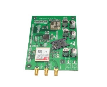
SMTFAB offers you safe and high-quality 14 Layer PCBs. Our company has the immense capacity to produce all kinds of Multilayer and Advanced PCBs.
Our circuit boards are used in diverse applications, including aeronautics, medical, and digital infrastructure.
In addition, we provide custom design and Reverse PCB Engineering for your convenience.
Call SMTFAB now for your 14 Layer PCB needs!
Types of 14 Layer PCBTo Generate Your Growth

Characterized as quite complex, the High-speed 14 Layer PCB powers applications like routers, motherboards and HDMI. SMTFAB assures quality because of the attention needed in impedance, signal interference and signal integrity aspects.

SMTFAB’s Presensitized 14 Layer PCBs is used because the photosensitive pre-coating helps make Customized PCBs easier to create. Designing a PCB like this is more accurate than using a toner. Nowadays presensitizing is common.

SMTFAB achieves the great quality of its Rigid-Flex 14 Layer PCB by being methodical in the lamination process. We pay attention to be sure the connection can withstand many times of flexing. Thie Rigid-Flex design fits better in irregularly shaped devices.

Rigid 14 Layer PCBs can be deployed in environments where the need for stability comes first. Our Rigid PCBs are inside CPU, laptops, electric vehicles, and amplifiers, to name a few devices.

SMTFAB’s Microvia 14 Layer PCB maximizes space so that the end product can fit into miniaturized devices. For instance, there is a demand for smaller medical devices using micro-electronics (e.g. insertable sensors).

Most Press-fit 14 Layer PCB customers demand the best PCB money can buy. Minimizing residue, advanced applications in the automotive and military field often demand the use of this kind of PCB.
SMTFAB is a Renown Producer of the 14 Layer PCB
Installing and building a 14 Layer PCB begins with the right method. At SMTFAB, we do not skip the crucial steps of PCB design, subtrate, inspection, and lamination.
You can see in this video that we thoroughly test all our 14 Layer PCBs before product roll-out. We lower the risk of PCB defects by following standard PCB inspections (AOI, E-test, etc.)
That is why you can trust SMTFAB for your order.

Related 14 Layer PCB


14 Layer PCB Production Details As Following Up
- Production Facility
- PCB Capabilities
- PCB Materials
- Shipping Methods
- Payment Methods
- Send Us Inquiry


| Item | Capability |
| Layer Count | 1-40layers |
| Base Material | KB、Shengyi、ShengyiSF305、FR408、FR408HR、IS410、FR406、GETEK、370HR、IT180A、Rogers4350B、Rogers4000、PTFE Laminates(Rogers series、Taconic series、Arlon series、Nelco series)、Rogers/Taconic/Arlon/Nelco laminate with FR-4 material(including partial Ro4350B hybrid laminating with FR-4) |
| Board Type | Backplane、HDI、High multi-layer 、blind&buried PCB、Embedded Capacitance、Embedded resistance board 、Heavy copper power PCB、Backdrill. |
| Board Thickness | 0.2-5.0mm |
| Copper Thickness | Min. 1/2 OZ, Max. 10 OZ |
| PTH Wall | 25um(1mil) |
| Maximum Board Size | 1100*500mm(43”*19”) |
| Min laser drilling size | 4mil |
| Min. Spacing/Tracing | 2.7mil/2.7mil |
| Solder Mask | Green, Black, Blue, Red, White, Yellow,Purple matte/glossy |
| Surface Treatment | Flash gold(electroplated gold)、ENIG、Hard gold、Flash gold、HASL Lead free、OSP、ENEPIG、Soft gold、Immersion silver、Immersion Tin、ENIG+OSP,ENIG+Gold finger,Flash gold(electroplated gold)+Gold finger,Immersion silver+Gold finger,Immersion Tin+Gold finger. |
| Min. Annular Ring | 3mil |
| Aspect ratio | 10:1(HASL Lead free、HASL Lead、ENIG、Immersion Tin、Immersion silver、ENEPIG);8:1(OSP) |
| Impedance control | ±5ohm(<50ohm), ±10%(≥50ohm) |
| Other Techniques | Blind/Buried Via |
| Gold Fingers | |
| Press Fit | |
| Via in Pad | |
| Electrical Test |
Here there’re many laminate material datasheets, they’re useful and helpful for you, please see them:
| SUPPLIER | PCB LAMINATE | TYPE | MATERIAL DATASHEET | TG | TD | DK(1MHZ) | DK(1GHZ) | DK(10GHZ) |
| KB | KB-6160 | FR4 | DOWNLOAD | 135 | 305 | 4.35 | – | – |
| KB-6160A | FR4 | DOWNLOAD | 135 | 305 | 4.35 | – | – | |
| KB-6160C | FR4 | DOWNLOAD | 135 | 314 | 4.7 | – | – | |
| KB-6150 KB-6150C | FR4 | DOWNLOAD | 132 | 305 | 4.6 | – | – | |
| KB-6164 | FR4 | DOWNLOAD | 142 | 330 | 4.8 | – | – | |
| KB-6164F | FR4 | DOWNLOAD | 145 | 340 | 4.8 | – | – | |
| KB-6165F | FR4 | DOWNLOAD | 150 | 346 | 4.8 | – | – | |
| KB-6167F | FR4 | DOWNLOAD | 170 | 349 | 4.8 | – | – | |
| SHENGYI | S1141 | FR4 | DOWNLOAD | 135 | 310 | 4.6 | – | – |
| S1141KF | FR4 | DOWNLOAD | 140 | 350 | 4.7 | – | – | |
| S1000 | FR4 | DOWNLOAD | 155 | 335 | 4.9 | – | – | |
| S1170 | FR4 | DOWNLOAD | 170 | 335 | 4.6 | – | – | |
| S1000-2 | FR4 | DOWNLOAD | 170 | 335 | 4.8 | – | – | |
| S1155 | FR4 | DOWNLOAD | 135 | 370 | 4.7 | – | – | |
| ITEQ | IT-158 | FR4 | DOWNLOAD | 150 | 340 | 4.6-4.8 | – | – |
| IT-180 | FR4 | DOWNLOAD | 180 | 350 | 4.5-4.7 | – | – | |
| TUC | TU-768 | FR4 | DOWNLOAD | 180 | 350 | – | 4.3-4.4 | 4.3 |
| TU-872 | Modified Epoxy | DOWNLOAD | 200 | 340 | – | 3.8-4.0 | 3.8 | |
| ROGERS | RO 3003 | Cer/PTFE | DOWNLOAD | – | 500 | – | – | 3 |
| RO 3010 | Cer/PTFE | DOWNLOAD | – | 500 | – | – | 10.2 | |
| RO 4003 | Hydrocarbon/Cer | DOWNLOAD | >280 | 425 | – | – | 3.38 | |
| RO 4350B | Hydrocarbon/Cer | DOWNLOAD | >280 | 390 | – | – | 3.48 | |
| RT/duroid 5880 | PTFE/Glass | DOWNLOAD | – | 500 | – | – | 2.2 | |
| ISOLA | Polyclad 370HR | FR4 | DOWNLOAD | 170 | 340 | 4.8-5.1 | – | – |
| FR406-HR | FR4 | DOWNLOAD | 190 | 325 | 3.91 | 3.86 | 3.81 | |
| FR408-HR | FR4 | DOWNLOAD | 200 | 360 | 3.72 | 3.69 | 3.65 | |
| P96 | Polyimide | DOWNLOAD | 260 | 416 | – | 3.78 | 3.73 | |
| Hitachi | MCL-BE- 67G | Modified Epoxy | DOWNLOAD | 140 | 340 | 4.9 | 4.4 | – |
| MCL-E-679F | FR4 | DOWNLOAD | 170 | 350 | 4.2-4.4 | 4.3-4.5 | – | |
| MCL-LX-67Y | Special Laminate | DOWNLOAD | 185-195 | 325-345 | – | 3.4-3.6 | – | |
| Nelco | N4000-13 | Modified Epoxy | DOWNLOAD | 210-240 | 365 | – | 3.7 | 3.6 |
| N4000-13EP | Modified Epoxy | DOWNLOAD | 210-240 | 350 | – | 3.4 | 3.2 | |
| N4000-13SI | Modified Epoxy | DOWNLOAD | 210-240 | 350 | – | 3.4 | 3.2 | |
| N4000-13EP SI | Modified Epoxy | DOWNLOAD | 210-240 | 350 | – | 3.4 | 3.2 | |
| Taconic | TLX-6 | PTFE | DOWNLOAD | – | – | – | – | 2.65 |
| TLX-7 | PTFE | DOWNLOAD | – | – | – | – | 2.6 | |
| TLX-8 | PTFE | DOWNLOAD | – | – | – | – | 2.55 | |
| TLX-9 | PTFE | DOWNLOAD | – | – | – | – | 2.45 | |
| RF35 | PTFE | DOWNLOAD | <315 | – | 3.5 | – | 3.5 | |
| TLC-27 | PTFE | DOWNLOAD | – | – | – | – | 2.75 | |
| TLC-30 | PTFE | DOWNLOAD | – | – | – | – | 3 | |
| TLC-32 | PTFE | DOWNLOAD | – | – | – | – | 3.2 | |
| Arlon | Arlon 25N | Cer | DOWNLOAD | 260 | – | – | – | 3.38 |
| Arlon 25FR | Cer | DOWNLOAD | 260 | – | – | – | 3.58 | |
| Arlon 33N | Polymide | DOWNLOAD | >250 | 353 | 4 | – | – | |
| Arlon 35N | Polymide | DOWNLOAD | >250 | 363 | 4.2 | – | – | |
| Arlon 85N | Polymide | DOWNLOAD | 250 | 387 | 4.2 | – | – | |
| Stablcor | ST325 | – | DOWNLOAD | Thermal conductivity:75w/m.k(with 1oz copper) | ||||
| ST10 | – | DOWNLOAD | Thermal conductivity:325w/m.k(with 1oz copper) | |||||
| Panasonic | R-1566W | FR4 | DOWNLOAD | 140 | 330 | 4.95 | 4.7 | 4.65 |
| Ventec | VT-901 | Polymide | DOWNLOAD | 250 | 390 | 4.2-4.5 | 4.0-4.3 | – |
| VT-90H | Polymide | DOWNLOAD | 250 | 390 | 4.2-4.5 | 4.0-4.3 | – | |
| Bergquist | ht-04503 | – | DOWNLOAD | Thermal conductivity:2.2w/m.k(with 1oz copper) | ||||
Delivery
SMTFAB offers flexible shipping methods for our customers, you may choose from one of the methods below.
1. DHL
DHL offers international express services in over 220 countries.
DHL partners with SMTFAB and offers very competitive rates to customers of SMTFAB.
It normally takes 3-7 business days for the package to be delivered around the world.

2. UPS
UPS gets the facts and figures about the world’s largest package delivery company and one of the leading global providers of specialized transportation and logistics services.
It normally takes 3-7 business days to deliver a package to most of the addresses in the world.

3. TNT
TNT has 56,000 employees in 61 countries.
It takes 4-9 business days to deliver the packages to the hands
of our customers.

4. FedEx
FedEx offers delivery solutions for customers around the world.
It takes 4-7 business days to deliver the packages to the hands
of our customers.

5. Air, Sea/Air, and Sea
If your order is of large volume with SMTFAB, you can also choose
to ship via air, sea/air combined, and sea when necessary.
Please contact your sales representative for shipping solutions.
Note: if you need others, please contact your sales representative for shipping solutions.
On our website you can use the following payment methods:
Telegraphic Transfer(TT): A telegraphic transfer (TT) is an electronic method of transferring funds utilized primarily for overseas wire transactions. It’s very convenient to transfer.
Bank/Wire transfer: To pay by wire transfer using your bank account, you need to visit your nearest bank branch with the wire transfer information. Your payment will be completed 3-5 business days after you have finished the money transfer.
Paypal: Pay easily, fast and secure with PayPal. many other credit and debit cards via PayPal.
Credit Card: You can pay with credit card: Visa, Visa Electron, MasterCard, Maestro.
[contact-form-7 id=”764″ title=”Quick Quote”]
14 Layer PCB Needs? Count on Us!
SMTFAB understands the complex requirements you have for 14 Layer PCBs. This type of Multilayer PCB is the prevailing one used for digital applications. Wireless connectivity is not possible without PCBs like these. Therefore, you really need a solid supplier of this product to be your partner in business.
- Proper layering method for prepreg and core
- Accurate application of adhesives
- Correct hole drilling
- Environmental compliance for PCB process + raw materials
- Use top-notch material (Rogers, Shengyi, Nan Ya, and others)
The 14 Layer PCB can be assembled using Surface Mount Technology (SMT) or Plated Through Hole method. It depends on what you prefer as a customer. We can adjust to what method you prefer depending on your budget because we put you on top priority.
For new orders, we can help with special designs, for example, Kicad PCB design. You can also ask for a quick quotation after giving us your Gerber file.
In the process of fulfilling your order, SMTFAB gives you the option of a Work-in-Progress weekly report. Gladly, our customer service staff will answer any forthcoming questions.
As for affordability, our price is unbeatable. You deserve great PCBs at a great price,

So, as you see, you have come to the right place for 14 Layer PCB needs. SMTFAB gives you advanced technology, help with your order, as well as a great price.
We are surely the number 1 company for your 14 Layer PCB bulk order, special project, OEM, or EMS PCB. You will be very happy doing business with us.
Call now!
14 Layer PCB: The Ultimate FAQ Guide
A printed circuit board is an indispensable part of electronic appliances. 14 layer PCB is a standard electric circuit to improve the functional properties of numerous applications. The features of this multilayer PCB are supremely compatible with digital electronics.
SMTFAB, based in China, is a solid manufacturer of 14 layer PCB. We have a deep understanding of your requirements for this circuit board. This FAQ guide will be a proper guide for you to know the ins and out of this multilayer PCB. Let’s make a move with us.
- What Is 14 Layer PCB?
- Which Types Of 14 Layer PCBs Are Mostly Used In Electronic Devices?
- What Are The Notable Benefits Of 14 Layer PCB?
- Where Do You Use 14 Layer PCBs?
- Which Factor Do You Need To Consider While Choosing a 14 Layer PCB Manufacturer?
- What Are The Major Differences Between A Single Layer And A 14 Layer PCB?
- How To Control Overheating In A 14 layer PCB Board?
- Which Materials Are Used In 14 Layer PCB fabrication?
- What Is The Right 14 Layer PCB Thickness?
- Which Surface Finish Is The Most Effective For 14 Layer PCB?
- Why Do You Need To Use Via-In-Pad In 14 Layer PCB Stackup?
- How Do You Compare Between 10 Layer And 14 Layer PCB?
- What are The Negative Sides Of A 14 Layer PCB?
- How To Design A 14 Layer HDI PCB?
- What Is The Quality Control Process Of Rigid-flex 14 Layer PCB?
- How To Maintain Impedance Stability In A 14 layer PCB Design?
- Which Component Mounting Is Ideal For High-frequency 14 Layer PCB?
What Is 14 Layer PCB?
14 layer PCB is an orthodox multilayer circuit board containing 14 layers. Here, the conductive and dielectric materials are placed in the core of the materials and arranged in 14 layers.
It is an effective PCB for those electronic applications where a low layer count of PCB is not sufficient. This PCB offers outstanding benefits to advanced electronic devices. Its well-designed stack-up and effective materials promote the product’s durability.
It is also reputable for carrying high current loads and controlling high power. Its flexible design allows the designer to apply a single connecting point. That means a 14 layer circuit board simplifies the design layout resulting in reducing the weight of the device.

14 Layer PCB
Which Types Of 14 Layer PCBs Are Mostly Used In Electronic Devices?
The 14 layer PCB consists of various worthwhile features which develop the device performance to the next level. It also offers versatility. Different types of 14 layer circuit boards are available in the market to generate your growth. Such as:
High-speed 14 layer PCB
This PCB is widely utilized in motherboards, routers, HDMI, etc. Though its design has an extra bit of complication, it ensures impressive signal integrity along with controlled impedance.
14 layer press-fit PCB
Usually, multilayer press-fit PCBs are used in the military and automotive sectors due to their robust characteristics. It has a commendable reputation for minimizing residue during manufacturing.
Presensitized 14 layer PCB
It is very common in electronic devices because of its supreme compatibility with custom solutions. This circuit board laminates hold a photosensitive pre-coating that plays a vital role in allowing customization.
14 layer Rigid-flex PCB
Rigid-flex 14 layer circuit board modules are used in applications that contain irregular shapes. These PCBs also ensure sufficient rigidity to withstand external pressures.
Microvia 14 layer PCB
Nowadays, smaller electronic applications are highly desired because of using micro-electronics. Microvia 14 layer circuit board is a good choice to optimize miniature designs.
Rigid 14 layer PCB
It offers reliable robustness in CPUs, amplifiers, electric vehicles, etc. It is designed in such a way that it remains stable in vulnerable environments.

High-frequency 14 Layer PCB
What Are The Notable Benefits Of 14 Layer PCB?
14 layer PCB is an outstanding circuit board of recent times. It offers tremendous advantages in electronic projects because of has useful features. Thus, it has become the most used multilayer PCB in the electronic world. The noteworthy benefits of this printed circuit board include-
High Durability
A 14 layer PCB is extremely durable by nature. It is tolerant to high heat and pressure while binding the PCB layers together.
This PCB is composed of effective dielectric materials. These PCB materials show magnificent resistance against thermal and mechanical pressures.
Besides, these have a reputation for handling moisture and dust properly. All of these characteristics improve the application’s durability to a great extent.
Lightweight
A 14 layer PCB enables the designer to deal with compact designs. It results in decreasing the weight of the device. So, electronic appliances become easy to handle and maintain.
Improved Functionality
A printed circuit board containing 14 layers offers top-class functionality during its operation. It improves the component’s effectiveness through successful thermal management and power supply.
Besides, high-frequency applications require multilayer designs for their optimization. In this case, 14 layer PCBs are the best choice for their premium data transmission systems.
Miniature Design
The modern electronics world is supportive of miniature designs. Here, this circuit board fulfills the demand of time with great reliability. Different types of 14 layer circuits support high-density layouts.
So, surface mount devices can be placed here with proper space management. This facility significantly enhances its acceptability in advanced designs.
High Current Conduction
Normally, multilayer PCBs are designed for improving current conduction capacity. 14 layer high-speed PCB designs also maintain proper trace dimensions and dielectric properties.
Thus, it controls impedance that leads to controlled current carrying. This PCB also prevents overloads and short circuits while carrying high current loads.
Flexible Connection
PCBs often suffer from multiple connecting points. But, 14 layer PCB is free from such suffering. Its connection is highly flexible. So, it allows connecting all components in a single point. That’s why its design becomes easier.
Top-class Reliability
This PCB ensures the integrity of signal transmission in between the PCB layers. It protects signal loss during data transferring.
Moreover, multilayer circuit boards manage to send data in a reliable path maintaining transfer protocol. So, you can be relaxed about the security of data transmission services in high-speed 14 layer PCB assembly.

14 Layer PCB Benefits
Where Do You Use 14 Layer PCBs?
14 layer PCB is an effective solution for designing high-density electronic applications. It has versatile uses in different fields of modern electronics. Here, the most significant applications of this PCB are listed for you.
- Power supply
- File Servers
- Amplifiers
- GPS technology
- HDMI
- Medical equipment
- Test instrument
- Fiber optic receptor
- Computers
- Weather analysis
- Industrial equipment
- Aerospace equipment
- Signal transmission
- Smartphones
- Data storage
- Central fire alarm
- Nuclear detection
Except for these, you can use this highly functional multilayer circuit board in military instruments, satellite mechanisms, atomic accelerators, etc. Its flexible design along with comparatively easy processing makes it compatible with so many sectors.

Widely Used 14 Layer Printed Circuit Board
Which Factor Do You Need To Consider While Choosing a 14 Layer PCB Manufacturer?
You should consider the following factors to choose a 14 layer PCB manufacturer in China.
- The ability of manufacturing IPC standard 14 layer PCB.
- Long experience of multilayer PCB assembly.
- Professional engineers
- Competitive product cost.
- Standard sales and technological supports
- Testing facility
- ODM and OEM services
- Reliable component sourcing.

Top-class 14 Layer PCB Assembly
What Are The Major Differences Between A Single Layer And A 14 Layer PCB?
Multilayer PCBs are more advantageous than single-layer PCBs. The major differences between 14 layer PCB and single layer PCB are-
- 14 layer circuit boards are suitable for small and lightweight designs. But, single-layer PCBs are used in heavy electronic productions.
- These PCBs ensure more reliable signal transmission than a single-layer PCB.
- In high-frequency applications, PCBs having 14 layers are obviously the best option.
- If you prefer a high data transmission rate, you need to choose 14 layer circuit modules rather than a single or double-layer PCB.
- In terms of cost performance, 14 layer PCB is highly effective. Though it is more expensive than a single-layer PCB, it offers better performance.
- Multilayer PCBs operating capacity is higher compared to a single layer circuit board.
- In versatile complex designs, PCB with 14 layers is more preferable.

Single Layer Vs 14 Layer PCB
How To Control Overheating In A 14 layer PCB Board?
The 14 layer PCB shows superb control over heat production in electronic gadgets. Its design supports the use of contact pads that act in distributing heat properly. So, PCB components don’t get affected by overheating.
Again, this PCB contains effective dielectric materials which show hysteresis to heat production. Thus, a 14 layer PCB can handle heavy current loads without causing damages.

14 Layer PCB Overheating Control
Which Materials Are Used In 14 Layer PCB fabrication?
The 14 layer PCB is constructed through non-conductive substrate materials. It also contains copper layers. The most used materials in this PCB fabrication are-
- FR4
- Composite epoxy materials (CEM-1, CEM-3)
- FR-3
- FR-4 TG 170
These materials ensure sufficient dielectric strength and thermal stability in this multilayer PCB.

14 Layer PCB High TG Materials
What Is The Right 14 Layer PCB Thickness?
The minimum value of 14 layer PCB thickness is 1.4mm. It can vary concerning the design requirements of your products. Proper thickness improves the dimensional stability and design quality of this PCB.
Since a PCB stack-up consists of various parts which have individual thickness. Like the finish portion usually has a low thickness. It is around 0.2mm-0.7mm.

14 Layer PCB Thickness
Which Surface Finish Is The Most Effective For 14 Layer PCB?
ENIG is the most worthwhile 14 layer PCB surface finish. This PCB is compatible with different metallic and organic coatings. But, electroless nickel immersion gold (ENIG) provides the best output in resisting corrosion of the PCB surface.
Here, the most notable benefits of this surface finish of 14 layer circuit board include-
Resistant To Decay
Here, a protective coating of nickel is used with copper and gold layers. This combination ensures superlative protection against surface decay due to chemical contamination. Thus, 14 layer PCB laminates remain functional over a long period.
Component Protection
ENIG protects the PCB components from oxidation. Usually, resistors, transistors, diodes, etc lose their functionality and longevity due to being oxidized. So, this metallic layer promotes the operating life of PCB components to a large extent.
Moreover, it supports the incorporation of conformal coating and resin on the 14 layer PCB surface. So, the circuit remains safe from moisture contamination.
Signal Transmission
This PCB surface finish ensures smooth signal transmission in multilayer designs. It is supportive of surface mount technology.
Besides, ENIG makes the PCB surface broad enough to place the components efficiently. Thus, it significantly promotes the data transfer rate.
Environment-friendly
ENIG is compatible with lead-free technology. That’s why it causes no considerable damage to the ecology.

14 Layer PCB Stackup With ENIG Surface Finish
Why Do You Need To Use Via-In-Pad In 14 Layer PCB Stackup?
In the 14 layer PCB stack-up, via-in-pad is plated and planarized over the copper surface. Though via-in-pad promotes the manufacturing cost, it includes several positive points to this circuit board. The most notable of them are-
Improved Heat Dissipation
Via-in-pad improves thermal management in multilayer circuit boards. It creates a smooth way to distribute additional heat and reduces the possibility of overheating.
High Routing Density
14 layer PCB contact pads ensure a reliable trace routing between the PCB layers. Its design is compatible with high-density PCB routing that makes it more effective in compact electronic projects.
Strong Pad Connections
Via-in-pad offers a strong connection between contact pads. This feature is important for sending data without interference. It also promotes signal quality to a certain extent.
BGA Efficiency
You can optimize the Ball Grid Array (BGA) placement by using via-in-pads on the PCB surface. It allows the designer to utilize the whole surface in lieu of the terminals. Thus, PCB components like microprocessors, transistors, etc can function more efficiently and last for a long time.
High-frequency Design
In the case of high-frequency 14 layer circuit boards, via-in-pad renders immense benefits for component mounting. It delivers a strong connection to both SMD and through-hole components. That means PCB vias significantly develop the device performance.

14 Layer PCB Vias
How Do You Compare Between 10 Layer And 14 Layer PCB?
10 layer and 14 layers PCB both are considered as multilayer PCB. But, these circuit boards have some core differences in their formation and performance. Such as:
PCB Stackup
10 layer PCB stack-up refers to a PCB containing 6 signal layers along with 4 planes. On the contrary, 14 layer PCB stack-up deals with 8 signal layers. A well-designed stack up with 14 layers is more suitable for complex applications.
Trace Routing
The trace routing density of a 14 layer PCB is higher than a 10 layer PCB.
Design
14 layer circuit board design involves prepreg that provides dielectric in the PCB layers. Besides, it offers a broad surface area for component placement.
On the contrary, 10 layer PCB designs offer dielectrics to a certain limit. They provide a thinner surface area compared to a 14 layer circuit design.
Current Conduction
In terms of current conduction, 14 layer circuits are more efficient compared to a PCB with 10 conductive layers.

High-Quality 10 Layer PCB
What are The Negative Sides Of A 14 Layer PCB?
A 14 layer PCB includes various positive features in numerous electronic applications. But, it has some negative sides as well. We intend to give you a clear concept of this PCB. So, some considerable limitations of a 14 layer circuit board are listed here for your proper understanding.
- Its manufacturing cost is high compared to a PCB having a low layer count.
- A 14 layer PCB board design layout is a little bit complicated.
- It takes a lot of time to repair this PCB due to its design complexity.
- The lead time of 14 layer circuit board manufacturing is high.
We are dealing with designing and supplying this PCB for quite a long term. Our products are supremely cost-effective. We have a great bunch of professional engineers to handle its design and repair. So, we can assure you of a minimum lead time of its manufacturing. Inquire about us today to experience the most preferred 14 layer PCB assembly.

Highly Functional 14 Layer PCB
How To Design A 14 Layer HDI PCB?
The most vital design techniques of a 14 layer HDI PCB include-
- First, determine proper trace dimensions and layer thickness. It is essential for achieving impedance stability.
- Determine the minimum space between the PCB layers. It will help to place differential pairs in HDI PCB designs.
- To get a fine pitch BGA routing, you should keep the PCB traces coupled under the ball grid array packages.
- For maintaining symmetrical design, mirror all of the bends on differential pairs.
- Use microvia-in-pad to ensure coupling of associated traces.
- When you are routing through 14 layer HDI PCB plane layers, always try to use anti-pad diameter.
- You must place pads in pairs between the PCB traces.

14 Layer HDI PCB Design
Except for these considerations, the basic process of designing 14 layers of HDI PCB is almost similar to other PCBs. Watch this video to know more about HDI PCB:
What Is The Quality Control Process Of Rigid-flex 14 Layer PCB?
Rigid-flex 14 layer PCB makes the electric circuits compatible with different fields. It offers supreme flexibility along with adequate rigidity in electronic devices. The rigid-flex feature is essential to turn this circuit board stretchable and bendable.
Its quality control is the combination of a series of work. You need to give proper attention to material selection, testing, handling, etc to maintain this top-class multilayer PCB.
PCB Materials
PCB materials used in a 14 layer PCB fabrication have a great impact on its quality control. These materials should have stable electronic characteristics. Such as low relative permittivity, high dielectric strength, high transition temperature, etc.
Component Sourcing
It is required to ensure the component sourcing from a reliable supplier. Besides, you must consider the component’s shelf life, UL rating, ingress protection rating, mounting process, etc while selecting components for 14 layer circuit boards.
Regular Maintenance
You can achieve a standard quality of this PCB if it goes through regular maintenance. You should inspect it at a regular interval to find out the defects.
Functional Test
A proper functional test provides the real behavior of a 14 layer PCB. If you want to be sure about its real-time performance in high vibration and thermal pressures, a functional test is a good process. You can get the opportunity to promote the quality by resolving the defective issues.
Proper Use
The quality of a multilayer PCB hampers due to its wrong use in most cases. You should follow the manufacturer’s guide while handling and storing a 14 layer PCB. Besides, don’t keep this circuit board in extreme heat.
Though it can tolerate extreme temperatures, this is not suitable for maintaining supreme quality. It damages the functionality and resistive power of the PCB materials.
How To Maintain Impedance Stability In A 14 layer PCB Design?
Impedance stability is a vital issue in 14 layer PCB manufacturing. That’s why you should take care of electrical and mechanical properties that influence impedance in PCB layers.
Impedance in the PCB transmission line depends on the following factors:
- Dielectric constant
- Dielectric thickness
- Copper thickness
- Trace width
- Temperature change
A low and stable dielectric constant (DK) is necessary for achieving impedance control in an electric circuit. So, you need to use the PCB materials which offer a stable DK value (3.6-6.0).
Again, lower dielectric thickness and wider trace width ensure sufficient insulation in the PCB layers of the 14 layer PCB stackup. These properties are also crucial for having a stable impedance.
Frequent temperature change is a harmful measure for this PCB. It causes drastic fluctuations in the electric properties of PCB materials. This results in high impedance and inhibits the current transfer between the PCB layers.
You need to constantly maintain a proper dimension to achieve the desired impedance value. Otherwise, you never maintain the quality of your electronic appliances. Watch this video to get a better idea about controlled impedance PCB routing:
Which Component Mounting Is Ideal For High-frequency 14 Layer PCB?
A 14 layer high-frequency PCB usually supports both surface mount technology (SMT) and through-hole technology (THT). You need to choose the suitable component mounting carefully. 14 layer PCB assembly offers the flexibility to the manufacturers to apply a required mounting process as per their requirement.
SMT is preferable to those applications where you need to ensure supreme durability and smooth signal transmission. This component mounting process is used in a maximum 14 layer circuit board assembly. Surface mount devices offer effective component connections with low maintenance costs.
Besides, SMDs are reputable for their commendable resistance against oxidation and mechanical stresses. These components are supportive of miniature designs. So, you can enjoy a lightweight circuit board by applying SMT.
On the contrary, THT is comparatively less-used in 14 layer PCB assembly. It is mainly applicable where extreme robustness is required. But, it is highly expensive compared to SMT. You should decide on your project’s demand.

14 Layer PCB Component Mounting
Conclusion
14 layer PCB features are robust enough to control the whole device and run it smoothly. Its dielectric materials and useful components promote the functionality of the entire project. SMTFAB manufactures the best 14 layer PCB at a great price.
We have tried to let you know all the necessary information about this PCB. Contact us immediately to boost up your special projects.
The Leader in 14 Layer PCB Fabrication in China
More than 3000 customers worldwide prefer to buy 14 Layer PCBs from SMTFAB. Our company offers custom PCB and PCB assembly.
- UL certified in US and Canada
- Active PCB West participant
- Bring you eco-friendly PCB products
- No delay and hassle-free delivery
- Implement sophisticated PCB manufacturing techniques
SMTFAB 14 Layer PCB – Maximize Your Business with Us
SMTFAB offers you safe and high-quality 14 Layer PCBs. Our company has the immense capacity to produce all kinds of Multilayer and Advanced PCBs.
Our circuit boards are used in diverse applications, including aeronautics, medical, and digital infrastructure.
In addition, we provide custom design and Reverse PCB Engineering for your convenience.
Call SMTFAB now for your 14 Layer PCB needs!
Types of 14 Layer PCBTo Generate Your Growth
Characterized as quite complex, the High-speed 14 Layer PCB powers applications like routers, motherboards and HDMI. SMTFAB assures quality because of the attention needed in impedance, signal interference and signal integrity aspects.
SMTFAB’s Presensitized 14 Layer PCBs is used because the photosensitive pre-coating helps make Customized PCBs easier to create. Designing a PCB like this is more accurate than using a toner. Nowadays presensitizing is common.
SMTFAB achieves the great quality of its Rigid-Flex 14 Layer PCB by being methodical in the lamination process. We pay attention to be sure the connection can withstand many times of flexing. Thie Rigid-Flex design fits better in irregularly shaped devices.
Rigid 14 Layer PCBs can be deployed in environments where the need for stability comes first. Our Rigid PCBs are inside CPU, laptops, electric vehicles, and amplifiers, to name a few devices.
SMTFAB’s Microvia 14 Layer PCB maximizes space so that the end product can fit into miniaturized devices. For instance, there is a demand for smaller medical devices using micro-electronics (e.g. insertable sensors).
Most Press-fit 14 Layer PCB customers demand the best PCB money can buy. Minimizing residue, advanced applications in the automotive and military field often demand the use of this kind of PCB.
SMTFAB is a Renown Producer of the 14 Layer PCB
Installing and building a 14 Layer PCB begins with the right method. At SMTFAB, we do not skip the crucial steps of PCB design, subtrate, inspection, and lamination.
You can see in this video that we thoroughly test all our 14 Layer PCBs before product roll-out. We lower the risk of PCB defects by following standard PCB inspections (AOI, E-test, etc.)
That is why you can trust SMTFAB for your order.
Related 14 Layer PCB
14 Layer PCB Production Details As Following Up
- Production Facility
- PCB Capabilities
- PCB Materials
- Shipping Methods
- Payment Methods
- Send Us Inquiry
| Item | Capability |
| Layer Count | 1-40layers |
| Base Material | KB、Shengyi、ShengyiSF305、FR408、FR408HR、IS410、FR406、GETEK、370HR、IT180A、Rogers4350B、Rogers4000、PTFE Laminates(Rogers series、Taconic series、Arlon series、Nelco series)、Rogers/Taconic/Arlon/Nelco laminate with FR-4 material(including partial Ro4350B hybrid laminating with FR-4) |
| Board Type | Backplane、HDI、High multi-layer 、blind&buried PCB、Embedded Capacitance、Embedded resistance board 、Heavy copper power PCB、Backdrill. |
| Board Thickness | 0.2-5.0mm |
| Copper Thickness | Min. 1/2 OZ, Max. 10 OZ |
| PTH Wall | 25um(1mil) |
| Maximum Board Size | 1100*500mm(43”*19”) |
| Min laser drilling size | 4mil |
| Min. Spacing/Tracing | 2.7mil/2.7mil |
| Solder Mask | Green, Black, Blue, Red, White, Yellow,Purple matte/glossy |
| Surface Treatment | Flash gold(electroplated gold)、ENIG、Hard gold、Flash gold、HASL Lead free、OSP、ENEPIG、Soft gold、Immersion silver、Immersion Tin、ENIG+OSP,ENIG+Gold finger,Flash gold(electroplated gold)+Gold finger,Immersion silver+Gold finger,Immersion Tin+Gold finger. |
| Min. Annular Ring | 3mil |
| Aspect ratio | 10:1(HASL Lead free、HASL Lead、ENIG、Immersion Tin、Immersion silver、ENEPIG);8:1(OSP) |
| Impedance control | ±5ohm(<50ohm), ±10%(≥50ohm) |
| Other Techniques | Blind/Buried Via |
| Gold Fingers | |
| Press Fit | |
| Via in Pad | |
| Electrical Test |
Here there’re many laminate material datasheets, they’re useful and helpful for you, please see them:
| SUPPLIER | PCB LAMINATE | TYPE | MATERIAL DATASHEET | TG | TD | DK(1MHZ) | DK(1GHZ) | DK(10GHZ) |
| KB | KB-6160 | FR4 | DOWNLOAD | 135 | 305 | 4.35 | – | – |
| KB-6160A | FR4 | DOWNLOAD | 135 | 305 | 4.35 | – | – | |
| KB-6160C | FR4 | DOWNLOAD | 135 | 314 | 4.7 | – | – | |
| KB-6150 KB-6150C | FR4 | DOWNLOAD | 132 | 305 | 4.6 | – | – | |
| KB-6164 | FR4 | DOWNLOAD | 142 | 330 | 4.8 | – | – | |
| KB-6164F | FR4 | DOWNLOAD | 145 | 340 | 4.8 | – | – | |
| KB-6165F | FR4 | DOWNLOAD | 150 | 346 | 4.8 | – | – | |
| KB-6167F | FR4 | DOWNLOAD | 170 | 349 | 4.8 | – | – | |
| SHENGYI | S1141 | FR4 | DOWNLOAD | 135 | 310 | 4.6 | – | – |
| S1141KF | FR4 | DOWNLOAD | 140 | 350 | 4.7 | – | – | |
| S1000 | FR4 | DOWNLOAD | 155 | 335 | 4.9 | – | – | |
| S1170 | FR4 | DOWNLOAD | 170 | 335 | 4.6 | – | – | |
| S1000-2 | FR4 | DOWNLOAD | 170 | 335 | 4.8 | – | – | |
| S1155 | FR4 | DOWNLOAD | 135 | 370 | 4.7 | – | – | |
| ITEQ | IT-158 | FR4 | DOWNLOAD | 150 | 340 | 4.6-4.8 | – | – |
| IT-180 | FR4 | DOWNLOAD | 180 | 350 | 4.5-4.7 | – | – | |
| TUC | TU-768 | FR4 | DOWNLOAD | 180 | 350 | – | 4.3-4.4 | 4.3 |
| TU-872 | Modified Epoxy | DOWNLOAD | 200 | 340 | – | 3.8-4.0 | 3.8 | |
| ROGERS | RO 3003 | Cer/PTFE | DOWNLOAD | – | 500 | – | – | 3 |
| RO 3010 | Cer/PTFE | DOWNLOAD | – | 500 | – | – | 10.2 | |
| RO 4003 | Hydrocarbon/Cer | DOWNLOAD | >280 | 425 | – | – | 3.38 | |
| RO 4350B | Hydrocarbon/Cer | DOWNLOAD | >280 | 390 | – | – | 3.48 | |
| RT/duroid 5880 | PTFE/Glass | DOWNLOAD | – | 500 | – | – | 2.2 | |
| ISOLA | Polyclad 370HR | FR4 | DOWNLOAD | 170 | 340 | 4.8-5.1 | – | – |
| FR406-HR | FR4 | DOWNLOAD | 190 | 325 | 3.91 | 3.86 | 3.81 | |
| FR408-HR | FR4 | DOWNLOAD | 200 | 360 | 3.72 | 3.69 | 3.65 | |
| P96 | Polyimide | DOWNLOAD | 260 | 416 | – | 3.78 | 3.73 | |
| Hitachi | MCL-BE- 67G | Modified Epoxy | DOWNLOAD | 140 | 340 | 4.9 | 4.4 | – |
| MCL-E-679F | FR4 | DOWNLOAD | 170 | 350 | 4.2-4.4 | 4.3-4.5 | – | |
| MCL-LX-67Y | Special Laminate | DOWNLOAD | 185-195 | 325-345 | – | 3.4-3.6 | – | |
| Nelco | N4000-13 | Modified Epoxy | DOWNLOAD | 210-240 | 365 | – | 3.7 | 3.6 |
| N4000-13EP | Modified Epoxy | DOWNLOAD | 210-240 | 350 | – | 3.4 | 3.2 | |
| N4000-13SI | Modified Epoxy | DOWNLOAD | 210-240 | 350 | – | 3.4 | 3.2 | |
| N4000-13EP SI | Modified Epoxy | DOWNLOAD | 210-240 | 350 | – | 3.4 | 3.2 | |
| Taconic | TLX-6 | PTFE | DOWNLOAD | – | – | – | – | 2.65 |
| TLX-7 | PTFE | DOWNLOAD | – | – | – | – | 2.6 | |
| TLX-8 | PTFE | DOWNLOAD | – | – | – | – | 2.55 | |
| TLX-9 | PTFE | DOWNLOAD | – | – | – | – | 2.45 | |
| RF35 | PTFE | DOWNLOAD | <315 | – | 3.5 | – | 3.5 | |
| TLC-27 | PTFE | DOWNLOAD | – | – | – | – | 2.75 | |
| TLC-30 | PTFE | DOWNLOAD | – | – | – | – | 3 | |
| TLC-32 | PTFE | DOWNLOAD | – | – | – | – | 3.2 | |
| Arlon | Arlon 25N | Cer | DOWNLOAD | 260 | – | – | – | 3.38 |
| Arlon 25FR | Cer | DOWNLOAD | 260 | – | – | – | 3.58 | |
| Arlon 33N | Polymide | DOWNLOAD | >250 | 353 | 4 | – | – | |
| Arlon 35N | Polymide | DOWNLOAD | >250 | 363 | 4.2 | – | – | |
| Arlon 85N | Polymide | DOWNLOAD | 250 | 387 | 4.2 | – | – | |
| Stablcor | ST325 | – | DOWNLOAD | Thermal conductivity:75w/m.k(with 1oz copper) | ||||
| ST10 | – | DOWNLOAD | Thermal conductivity:325w/m.k(with 1oz copper) | |||||
| Panasonic | R-1566W | FR4 | DOWNLOAD | 140 | 330 | 4.95 | 4.7 | 4.65 |
| Ventec | VT-901 | Polymide | DOWNLOAD | 250 | 390 | 4.2-4.5 | 4.0-4.3 | – |
| VT-90H | Polymide | DOWNLOAD | 250 | 390 | 4.2-4.5 | 4.0-4.3 | – | |
| Bergquist | ht-04503 | – | DOWNLOAD | Thermal conductivity:2.2w/m.k(with 1oz copper) | ||||
Delivery
SMTFAB offers flexible shipping methods for our customers, you may choose from one of the methods below.
1. DHL
DHL offers international express services in over 220 countries.
DHL partners with SMTFAB and offers very competitive rates to customers of SMTFAB.
It normally takes 3-7 business days for the package to be delivered around the world.
2. UPS
UPS gets the facts and figures about the world’s largest package delivery company and one of the leading global providers of specialized transportation and logistics services.
It normally takes 3-7 business days to deliver a package to most of the addresses in the world.
3. TNT
TNT has 56,000 employees in 61 countries.
It takes 4-9 business days to deliver the packages to the hands
of our customers.
4. FedEx
FedEx offers delivery solutions for customers around the world.
It takes 4-7 business days to deliver the packages to the hands
of our customers.
5. Air, Sea/Air, and Sea
If your order is of large volume with SMTFAB, you can also choose
to ship via air, sea/air combined, and sea when necessary.
Please contact your sales representative for shipping solutions.
Note: if you need others, please contact your sales representative for shipping solutions.
On our website you can use the following payment methods:
Telegraphic Transfer(TT): A telegraphic transfer (TT) is an electronic method of transferring funds utilized primarily for overseas wire transactions. It’s very convenient to transfer.
Bank/Wire transfer: To pay by wire transfer using your bank account, you need to visit your nearest bank branch with the wire transfer information. Your payment will be completed 3-5 business days after you have finished the money transfer.
Paypal: Pay easily, fast and secure with PayPal. many other credit and debit cards via PayPal.
Credit Card: You can pay with credit card: Visa, Visa Electron, MasterCard, Maestro.
[contact-form-7 id=”764″ title=”Quick Quote”]
14 Layer PCB Needs? Count on Us!
SMTFAB understands the complex requirements you have for 14 Layer PCBs. This type of Multilayer PCB is the prevailing one used for digital applications. Wireless connectivity is not possible without PCBs like these. Therefore, you really need a solid supplier of this product to be your partner in business.
- Proper layering method for prepreg and core
- Accurate application of adhesives
- Correct hole drilling
- Environmental compliance for PCB process + raw materials
- Use top-notch material (Rogers, Shengyi, Nan Ya, and others)
The 14 Layer PCB can be assembled using Surface Mount Technology (SMT) or Plated Through Hole method. It depends on what you prefer as a customer. We can adjust to what method you prefer depending on your budget because we put you on top priority.
For new orders, we can help with special designs, for example, Kicad PCB design. You can also ask for a quick quotation after giving us your Gerber file.
In the process of fulfilling your order, SMTFAB gives you the option of a Work-in-Progress weekly report. Gladly, our customer service staff will answer any forthcoming questions.
As for affordability, our price is unbeatable. You deserve great PCBs at a great price,
So, as you see, you have come to the right place for 14 Layer PCB needs. SMTFAB gives you advanced technology, help with your order, as well as a great price.
We are surely the number 1 company for your 14 Layer PCB bulk order, special project, OEM, or EMS PCB. You will be very happy doing business with us.
Call now!
14 Layer PCB: The Ultimate FAQ Guide
A printed circuit board is an indispensable part of electronic appliances. 14 layer PCB is a standard electric circuit to improve the functional properties of numerous applications. The features of this multilayer PCB are supremely compatible with digital electronics.
SMTFAB, based in China, is a solid manufacturer of 14 layer PCB. We have a deep understanding of your requirements for this circuit board. This FAQ guide will be a proper guide for you to know the ins and out of this multilayer PCB. Let’s make a move with us.
- What Is 14 Layer PCB?
- Which Types Of 14 Layer PCBs Are Mostly Used In Electronic Devices?
- What Are The Notable Benefits Of 14 Layer PCB?
- Where Do You Use 14 Layer PCBs?
- Which Factor Do You Need To Consider While Choosing a 14 Layer PCB Manufacturer?
- What Are The Major Differences Between A Single Layer And A 14 Layer PCB?
- How To Control Overheating In A 14 layer PCB Board?
- Which Materials Are Used In 14 Layer PCB fabrication?
- What Is The Right 14 Layer PCB Thickness?
- Which Surface Finish Is The Most Effective For 14 Layer PCB?
- Why Do You Need To Use Via-In-Pad In 14 Layer PCB Stackup?
- How Do You Compare Between 10 Layer And 14 Layer PCB?
- What are The Negative Sides Of A 14 Layer PCB?
- How To Design A 14 Layer HDI PCB?
- What Is The Quality Control Process Of Rigid-flex 14 Layer PCB?
- How To Maintain Impedance Stability In A 14 layer PCB Design?
- Which Component Mounting Is Ideal For High-frequency 14 Layer PCB?
What Is 14 Layer PCB?
14 layer PCB is an orthodox multilayer circuit board containing 14 layers. Here, the conductive and dielectric materials are placed in the core of the materials and arranged in 14 layers.
It is an effective PCB for those electronic applications where a low layer count of PCB is not sufficient. This PCB offers outstanding benefits to advanced electronic devices. Its well-designed stack-up and effective materials promote the product’s durability.
It is also reputable for carrying high current loads and controlling high power. Its flexible design allows the designer to apply a single connecting point. That means a 14 layer circuit board simplifies the design layout resulting in reducing the weight of the device.
14 Layer PCB
Which Types Of 14 Layer PCBs Are Mostly Used In Electronic Devices?
The 14 layer PCB consists of various worthwhile features which develop the device performance to the next level. It also offers versatility. Different types of 14 layer circuit boards are available in the market to generate your growth. Such as:
High-speed 14 layer PCB
This PCB is widely utilized in motherboards, routers, HDMI, etc. Though its design has an extra bit of complication, it ensures impressive signal integrity along with controlled impedance.
14 layer press-fit PCB
Usually, multilayer press-fit PCBs are used in the military and automotive sectors due to their robust characteristics. It has a commendable reputation for minimizing residue during manufacturing.
Presensitized 14 layer PCB
It is very common in electronic devices because of its supreme compatibility with custom solutions. This circuit board laminates hold a photosensitive pre-coating that plays a vital role in allowing customization.
14 layer Rigid-flex PCB
Rigid-flex 14 layer circuit board modules are used in applications that contain irregular shapes. These PCBs also ensure sufficient rigidity to withstand external pressures.
Microvia 14 layer PCB
Nowadays, smaller electronic applications are highly desired because of using micro-electronics. Microvia 14 layer circuit board is a good choice to optimize miniature designs.
Rigid 14 layer PCB
It offers reliable robustness in CPUs, amplifiers, electric vehicles, etc. It is designed in such a way that it remains stable in vulnerable environments.
High-frequency 14 Layer PCB
What Are The Notable Benefits Of 14 Layer PCB?
14 layer PCB is an outstanding circuit board of recent times. It offers tremendous advantages in electronic projects because of has useful features. Thus, it has become the most used multilayer PCB in the electronic world. The noteworthy benefits of this printed circuit board include-
High Durability
A 14 layer PCB is extremely durable by nature. It is tolerant to high heat and pressure while binding the PCB layers together.
This PCB is composed of effective dielectric materials. These PCB materials show magnificent resistance against thermal and mechanical pressures.
Besides, these have a reputation for handling moisture and dust properly. All of these characteristics improve the application’s durability to a great extent.
Lightweight
A 14 layer PCB enables the designer to deal with compact designs. It results in decreasing the weight of the device. So, electronic appliances become easy to handle and maintain.
Improved Functionality
A printed circuit board containing 14 layers offers top-class functionality during its operation. It improves the component’s effectiveness through successful thermal management and power supply.
Besides, high-frequency applications require multilayer designs for their optimization. In this case, 14 layer PCBs are the best choice for their premium data transmission systems.
Miniature Design
The modern electronics world is supportive of miniature designs. Here, this circuit board fulfills the demand of time with great reliability. Different types of 14 layer circuits support high-density layouts.
So, surface mount devices can be placed here with proper space management. This facility significantly enhances its acceptability in advanced designs.
High Current Conduction
Normally, multilayer PCBs are designed for improving current conduction capacity. 14 layer high-speed PCB designs also maintain proper trace dimensions and dielectric properties.
Thus, it controls impedance that leads to controlled current carrying. This PCB also prevents overloads and short circuits while carrying high current loads.
Flexible Connection
PCBs often suffer from multiple connecting points. But, 14 layer PCB is free from such suffering. Its connection is highly flexible. So, it allows connecting all components in a single point. That’s why its design becomes easier.
Top-class Reliability
This PCB ensures the integrity of signal transmission in between the PCB layers. It protects signal loss during data transferring.
Moreover, multilayer circuit boards manage to send data in a reliable path maintaining transfer protocol. So, you can be relaxed about the security of data transmission services in high-speed 14 layer PCB assembly.
14 Layer PCB Benefits
Where Do You Use 14 Layer PCBs?
14 layer PCB is an effective solution for designing high-density electronic applications. It has versatile uses in different fields of modern electronics. Here, the most significant applications of this PCB are listed for you.
- Power supply
- File Servers
- Amplifiers
- GPS technology
- HDMI
- Medical equipment
- Test instrument
- Fiber optic receptor
- Computers
- Weather analysis
- Industrial equipment
- Aerospace equipment
- Signal transmission
- Smartphones
- Data storage
- Central fire alarm
- Nuclear detection
Except for these, you can use this highly functional multilayer circuit board in military instruments, satellite mechanisms, atomic accelerators, etc. Its flexible design along with comparatively easy processing makes it compatible with so many sectors.
Widely Used 14 Layer Printed Circuit Board
Which Factor Do You Need To Consider While Choosing a 14 Layer PCB Manufacturer?
You should consider the following factors to choose a 14 layer PCB manufacturer in China.
- The ability of manufacturing IPC standard 14 layer PCB.
- Long experience of multilayer PCB assembly.
- Professional engineers
- Competitive product cost.
- Standard sales and technological supports
- Testing facility
- ODM and OEM services
- Reliable component sourcing.
Top-class 14 Layer PCB Assembly
What Are The Major Differences Between A Single Layer And A 14 Layer PCB?
Multilayer PCBs are more advantageous than single-layer PCBs. The major differences between 14 layer PCB and single layer PCB are-
- 14 layer circuit boards are suitable for small and lightweight designs. But, single-layer PCBs are used in heavy electronic productions.
- These PCBs ensure more reliable signal transmission than a single-layer PCB.
- In high-frequency applications, PCBs having 14 layers are obviously the best option.
- If you prefer a high data transmission rate, you need to choose 14 layer circuit modules rather than a single or double-layer PCB.
- In terms of cost performance, 14 layer PCB is highly effective. Though it is more expensive than a single-layer PCB, it offers better performance.
- Multilayer PCBs operating capacity is higher compared to a single layer circuit board.
- In versatile complex designs, PCB with 14 layers is more preferable.
Single Layer Vs 14 Layer PCB
How To Control Overheating In A 14 layer PCB Board?
The 14 layer PCB shows superb control over heat production in electronic gadgets. Its design supports the use of contact pads that act in distributing heat properly. So, PCB components don’t get affected by overheating.
Again, this PCB contains effective dielectric materials which show hysteresis to heat production. Thus, a 14 layer PCB can handle heavy current loads without causing damages.
14 Layer PCB Overheating Control
Which Materials Are Used In 14 Layer PCB fabrication?
The 14 layer PCB is constructed through non-conductive substrate materials. It also contains copper layers. The most used materials in this PCB fabrication are-
- FR4
- Composite epoxy materials (CEM-1, CEM-3)
- FR-3
- FR-4 TG 170
These materials ensure sufficient dielectric strength and thermal stability in this multilayer PCB.
14 Layer PCB High TG Materials
What Is The Right 14 Layer PCB Thickness?
The minimum value of 14 layer PCB thickness is 1.4mm. It can vary concerning the design requirements of your products. Proper thickness improves the dimensional stability and design quality of this PCB.
Since a PCB stack-up consists of various parts which have individual thickness. Like the finish portion usually has a low thickness. It is around 0.2mm-0.7mm.
14 Layer PCB Thickness
Which Surface Finish Is The Most Effective For 14 Layer PCB?
ENIG is the most worthwhile 14 layer PCB surface finish. This PCB is compatible with different metallic and organic coatings. But, electroless nickel immersion gold (ENIG) provides the best output in resisting corrosion of the PCB surface.
Here, the most notable benefits of this surface finish of 14 layer circuit board include-
Resistant To Decay
Here, a protective coating of nickel is used with copper and gold layers. This combination ensures superlative protection against surface decay due to chemical contamination. Thus, 14 layer PCB laminates remain functional over a long period.
Component Protection
ENIG protects the PCB components from oxidation. Usually, resistors, transistors, diodes, etc lose their functionality and longevity due to being oxidized. So, this metallic layer promotes the operating life of PCB components to a large extent.
Moreover, it supports the incorporation of conformal coating and resin on the 14 layer PCB surface. So, the circuit remains safe from moisture contamination.
Signal Transmission
This PCB surface finish ensures smooth signal transmission in multilayer designs. It is supportive of surface mount technology.
Besides, ENIG makes the PCB surface broad enough to place the components efficiently. Thus, it significantly promotes the data transfer rate.
Environment-friendly
ENIG is compatible with lead-free technology. That’s why it causes no considerable damage to the ecology.
14 Layer PCB Stackup With ENIG Surface Finish
Why Do You Need To Use Via-In-Pad In 14 Layer PCB Stackup?
In the 14 layer PCB stack-up, via-in-pad is plated and planarized over the copper surface. Though via-in-pad promotes the manufacturing cost, it includes several positive points to this circuit board. The most notable of them are-
Improved Heat Dissipation
Via-in-pad improves thermal management in multilayer circuit boards. It creates a smooth way to distribute additional heat and reduces the possibility of overheating.
High Routing Density
14 layer PCB contact pads ensure a reliable trace routing between the PCB layers. Its design is compatible with high-density PCB routing that makes it more effective in compact electronic projects.
Strong Pad Connections
Via-in-pad offers a strong connection between contact pads. This feature is important for sending data without interference. It also promotes signal quality to a certain extent.
BGA Efficiency
You can optimize the Ball Grid Array (BGA) placement by using via-in-pads on the PCB surface. It allows the designer to utilize the whole surface in lieu of the terminals. Thus, PCB components like microprocessors, transistors, etc can function more efficiently and last for a long time.
High-frequency Design
In the case of high-frequency 14 layer circuit boards, via-in-pad renders immense benefits for component mounting. It delivers a strong connection to both SMD and through-hole components. That means PCB vias significantly develop the device performance.
14 Layer PCB Vias
How Do You Compare Between 10 Layer And 14 Layer PCB?
10 layer and 14 layers PCB both are considered as multilayer PCB. But, these circuit boards have some core differences in their formation and performance. Such as:
PCB Stackup
10 layer PCB stack-up refers to a PCB containing 6 signal layers along with 4 planes. On the contrary, 14 layer PCB stack-up deals with 8 signal layers. A well-designed stack up with 14 layers is more suitable for complex applications.
Trace Routing
The trace routing density of a 14 layer PCB is higher than a 10 layer PCB.
Design
14 layer circuit board design involves prepreg that provides dielectric in the PCB layers. Besides, it offers a broad surface area for component placement.
On the contrary, 10 layer PCB designs offer dielectrics to a certain limit. They provide a thinner surface area compared to a 14 layer circuit design.
Current Conduction
In terms of current conduction, 14 layer circuits are more efficient compared to a PCB with 10 conductive layers.
High-Quality 10 Layer PCB
What are The Negative Sides Of A 14 Layer PCB?
A 14 layer PCB includes various positive features in numerous electronic applications. But, it has some negative sides as well. We intend to give you a clear concept of this PCB. So, some considerable limitations of a 14 layer circuit board are listed here for your proper understanding.
- Its manufacturing cost is high compared to a PCB having a low layer count.
- A 14 layer PCB board design layout is a little bit complicated.
- It takes a lot of time to repair this PCB due to its design complexity.
- The lead time of 14 layer circuit board manufacturing is high.
We are dealing with designing and supplying this PCB for quite a long term. Our products are supremely cost-effective. We have a great bunch of professional engineers to handle its design and repair. So, we can assure you of a minimum lead time of its manufacturing. Inquire about us today to experience the most preferred 14 layer PCB assembly.
Highly Functional 14 Layer PCB
How To Design A 14 Layer HDI PCB?
The most vital design techniques of a 14 layer HDI PCB include-
- First, determine proper trace dimensions and layer thickness. It is essential for achieving impedance stability.
- Determine the minimum space between the PCB layers. It will help to place differential pairs in HDI PCB designs.
- To get a fine pitch BGA routing, you should keep the PCB traces coupled under the ball grid array packages.
- For maintaining symmetrical design, mirror all of the bends on differential pairs.
- Use microvia-in-pad to ensure coupling of associated traces.
- When you are routing through 14 layer HDI PCB plane layers, always try to use anti-pad diameter.
- You must place pads in pairs between the PCB traces.
14 Layer HDI PCB Design
Except for these considerations, the basic process of designing 14 layers of HDI PCB is almost similar to other PCBs. Watch this video to know more about HDI PCB:
What Is The Quality Control Process Of Rigid-flex 14 Layer PCB?
Rigid-flex 14 layer PCB makes the electric circuits compatible with different fields. It offers supreme flexibility along with adequate rigidity in electronic devices. The rigid-flex feature is essential to turn this circuit board stretchable and bendable.
Its quality control is the combination of a series of work. You need to give proper attention to material selection, testing, handling, etc to maintain this top-class multilayer PCB.
PCB Materials
PCB materials used in a 14 layer PCB fabrication have a great impact on its quality control. These materials should have stable electronic characteristics. Such as low relative permittivity, high dielectric strength, high transition temperature, etc.
Component Sourcing
It is required to ensure the component sourcing from a reliable supplier. Besides, you must consider the component’s shelf life, UL rating, ingress protection rating, mounting process, etc while selecting components for 14 layer circuit boards.
Regular Maintenance
You can achieve a standard quality of this PCB if it goes through regular maintenance. You should inspect it at a regular interval to find out the defects.
Functional Test
A proper functional test provides the real behavior of a 14 layer PCB. If you want to be sure about its real-time performance in high vibration and thermal pressures, a functional test is a good process. You can get the opportunity to promote the quality by resolving the defective issues.
Proper Use
The quality of a multilayer PCB hampers due to its wrong use in most cases. You should follow the manufacturer’s guide while handling and storing a 14 layer PCB. Besides, don’t keep this circuit board in extreme heat.
Though it can tolerate extreme temperatures, this is not suitable for maintaining supreme quality. It damages the functionality and resistive power of the PCB materials.
How To Maintain Impedance Stability In A 14 layer PCB Design?
Impedance stability is a vital issue in 14 layer PCB manufacturing. That’s why you should take care of electrical and mechanical properties that influence impedance in PCB layers.
Impedance in the PCB transmission line depends on the following factors:
- Dielectric constant
- Dielectric thickness
- Copper thickness
- Trace width
- Temperature change
A low and stable dielectric constant (DK) is necessary for achieving impedance control in an electric circuit. So, you need to use the PCB materials which offer a stable DK value (3.6-6.0).
Again, lower dielectric thickness and wider trace width ensure sufficient insulation in the PCB layers of the 14 layer PCB stackup. These properties are also crucial for having a stable impedance.
Frequent temperature change is a harmful measure for this PCB. It causes drastic fluctuations in the electric properties of PCB materials. This results in high impedance and inhibits the current transfer between the PCB layers.
You need to constantly maintain a proper dimension to achieve the desired impedance value. Otherwise, you never maintain the quality of your electronic appliances. Watch this video to get a better idea about controlled impedance PCB routing:
Which Component Mounting Is Ideal For High-frequency 14 Layer PCB?
A 14 layer high-frequency PCB usually supports both surface mount technology (SMT) and through-hole technology (THT). You need to choose the suitable component mounting carefully. 14 layer PCB assembly offers the flexibility to the manufacturers to apply a required mounting process as per their requirement.
SMT is preferable to those applications where you need to ensure supreme durability and smooth signal transmission. This component mounting process is used in a maximum 14 layer circuit board assembly. Surface mount devices offer effective component connections with low maintenance costs.
Besides, SMDs are reputable for their commendable resistance against oxidation and mechanical stresses. These components are supportive of miniature designs. So, you can enjoy a lightweight circuit board by applying SMT.
On the contrary, THT is comparatively less-used in 14 layer PCB assembly. It is mainly applicable where extreme robustness is required. But, it is highly expensive compared to SMT. You should decide on your project’s demand.
14 Layer PCB Component Mounting
Conclusion
14 layer PCB features are robust enough to control the whole device and run it smoothly. Its dielectric materials and useful components promote the functionality of the entire project. SMTFAB manufactures the best 14 layer PCB at a great price.
We have tried to let you know all the necessary information about this PCB. Contact us immediately to boost up your special projects.
The Leader in 14 Layer PCB Fabrication in China
More than 3000 customers worldwide prefer to buy 14 Layer PCBs from SMTFAB. Our company offers custom PCB and PCB assembly.
- UL certified in US and Canada
- Active PCB West participant
- Bring you eco-friendly PCB products
- No delay and hassle-free delivery
- Implement sophisticated PCB manufacturing techniques
SMTFAB 14 Layer PCB – Maximize Your Business with Us
SMTFAB offers you safe and high-quality 14 Layer PCBs. Our company has the immense capacity to produce all kinds of Multilayer and Advanced PCBs.
Our circuit boards are used in diverse applications, including aeronautics, medical, and digital infrastructure.
In addition, we provide custom design and Reverse PCB Engineering for your convenience.
Call SMTFAB now for your 14 Layer PCB needs!
Types of 14 Layer PCBTo Generate Your Growth
Characterized as quite complex, the High-speed 14 Layer PCB powers applications like routers, motherboards and HDMI. SMTFAB assures quality because of the attention needed in impedance, signal interference and signal integrity aspects.
SMTFAB’s Presensitized 14 Layer PCBs is used because the photosensitive pre-coating helps make Customized PCBs easier to create. Designing a PCB like this is more accurate than using a toner. Nowadays presensitizing is common.
SMTFAB achieves the great quality of its Rigid-Flex 14 Layer PCB by being methodical in the lamination process. We pay attention to be sure the connection can withstand many times of flexing. Thie Rigid-Flex design fits better in irregularly shaped devices.
Rigid 14 Layer PCBs can be deployed in environments where the need for stability comes first. Our Rigid PCBs are inside CPU, laptops, electric vehicles, and amplifiers, to name a few devices.
SMTFAB’s Microvia 14 Layer PCB maximizes space so that the end product can fit into miniaturized devices. For instance, there is a demand for smaller medical devices using micro-electronics (e.g. insertable sensors).
Most Press-fit 14 Layer PCB customers demand the best PCB money can buy. Minimizing residue, advanced applications in the automotive and military field often demand the use of this kind of PCB.
Types of 14 Layer PCBTo Generate Your Growth
Types of 14 Layer PCBTo Generate Your Growth
Characterized as quite complex, the High-speed 14 Layer PCB powers applications like routers, motherboards and HDMI. SMTFAB assures quality because of the attention needed in impedance, signal interference and signal integrity aspects.
Characterized as quite complex, the High-speed 14 Layer PCB powers applications like routers, motherboards and HDMI. SMTFAB assures quality because of the attention needed in impedance, signal interference and signal integrity aspects.
Characterized as quite complex, the High-speed 14 Layer PCB powers applications like routers, motherboards and HDMI. SMTFAB assures quality because of the attention needed in impedance, signal interference and signal integrity aspects.
Characterized as quite complex, the High-speed 14 Layer PCB powers applications like routers, motherboards and HDMI. SMTFAB assures quality because of the attention needed in impedance, signal interference and signal integrity aspects.
SMTFAB’s Presensitized 14 Layer PCBs is used because the photosensitive pre-coating helps make Customized PCBs easier to create. Designing a PCB like this is more accurate than using a toner. Nowadays presensitizing is common.
SMTFAB’s Presensitized 14 Layer PCBs is used because the photosensitive pre-coating helps make Customized PCBs easier to create. Designing a PCB like this is more accurate than using a toner. Nowadays presensitizing is common.
SMTFAB’s Presensitized 14 Layer PCBs is used because the photosensitive pre-coating helps make Customized PCBs easier to create. Designing a PCB like this is more accurate than using a toner. Nowadays presensitizing is common.
SMTFAB’s Presensitized 14 Layer PCBs is used because the photosensitive pre-coating helps make Customized PCBs easier to create. Designing a PCB like this is more accurate than using a toner. Nowadays presensitizing is common.
SMTFAB achieves the great quality of its Rigid-Flex 14 Layer PCB by being methodical in the lamination process. We pay attention to be sure the connection can withstand many times of flexing. Thie Rigid-Flex design fits better in irregularly shaped devices.
SMTFAB achieves the great quality of its Rigid-Flex 14 Layer PCB by being methodical in the lamination process. We pay attention to be sure the connection can withstand many times of flexing. Thie Rigid-Flex design fits better in irregularly shaped devices.
SMTFAB achieves the great quality of its Rigid-Flex 14 Layer PCB by being methodical in the lamination process. We pay attention to be sure the connection can withstand many times of flexing. Thie Rigid-Flex design fits better in irregularly shaped devices.
SMTFAB achieves the great quality of its Rigid-Flex 14 Layer PCB by being methodical in the lamination process. We pay attention to be sure the connection can withstand many times of flexing. Thie Rigid-Flex design fits better in irregularly shaped devices.
Rigid 14 Layer PCBs can be deployed in environments where the need for stability comes first. Our Rigid PCBs are inside CPU, laptops, electric vehicles, and amplifiers, to name a few devices.
Rigid 14 Layer PCBs can be deployed in environments where the need for stability comes first. Our Rigid PCBs are inside CPU, laptops, electric vehicles, and amplifiers, to name a few devices.
Rigid 14 Layer PCBs can be deployed in environments where the need for stability comes first. Our Rigid PCBs are inside CPU, laptops, electric vehicles, and amplifiers, to name a few devices.
Rigid 14 Layer PCBs can be deployed in environments where the need for stability comes first. Our Rigid PCBs are inside CPU, laptops, electric vehicles, and amplifiers, to name a few devices.
SMTFAB’s Microvia 14 Layer PCB maximizes space so that the end product can fit into miniaturized devices. For instance, there is a demand for smaller medical devices using micro-electronics (e.g. insertable sensors).
SMTFAB’s Microvia 14 Layer PCB maximizes space so that the end product can fit into miniaturized devices. For instance, there is a demand for smaller medical devices using micro-electronics (e.g. insertable sensors).
SMTFAB’s Microvia 14 Layer PCB maximizes space so that the end product can fit into miniaturized devices. For instance, there is a demand for smaller medical devices using micro-electronics (e.g. insertable sensors).
SMTFAB’s Microvia 14 Layer PCB maximizes space so that the end product can fit into miniaturized devices. For instance, there is a demand for smaller medical devices using micro-electronics (e.g. insertable sensors).
Most Press-fit 14 Layer PCB customers demand the best PCB money can buy. Minimizing residue, advanced applications in the automotive and military field often demand the use of this kind of PCB.
Most Press-fit 14 Layer PCB customers demand the best PCB money can buy. Minimizing residue, advanced applications in the automotive and military field often demand the use of this kind of PCB.
Most Press-fit 14 Layer PCB customers demand the best PCB money can buy. Minimizing residue, advanced applications in the automotive and military field often demand the use of this kind of PCB.
Most Press-fit 14 Layer PCB customers demand the best PCB money can buy. Minimizing residue, advanced applications in the automotive and military field often demand the use of this kind of PCB.
SMTFAB is a Renown Producer of the 14 Layer PCB
Installing and building a 14 Layer PCB begins with the right method. At SMTFAB, we do not skip the crucial steps of PCB design, subtrate, inspection, and lamination.
You can see in this video that we thoroughly test all our 14 Layer PCBs before product roll-out. We lower the risk of PCB defects by following standard PCB inspections (AOI, E-test, etc.)
That is why you can trust SMTFAB for your order.
Related 14 Layer PCB
Related 14 Layer PCB
Related 14 Layer PCB
14 Layer PCB Production Details As Following Up
- Production Facility
- PCB Capabilities
- PCB Materials
- Shipping Methods
- Payment Methods
- Send Us Inquiry
| Item | Capability |
| Layer Count | 1-40layers |
| Base Material | KB、Shengyi、ShengyiSF305、FR408、FR408HR、IS410、FR406、GETEK、370HR、IT180A、Rogers4350B、Rogers4000、PTFE Laminates(Rogers series、Taconic series、Arlon series、Nelco series)、Rogers/Taconic/Arlon/Nelco laminate with FR-4 material(including partial Ro4350B hybrid laminating with FR-4) |
| Board Type | Backplane、HDI、High multi-layer 、blind&buried PCB、Embedded Capacitance、Embedded resistance board 、Heavy copper power PCB、Backdrill. |
| Board Thickness | 0.2-5.0mm |
| Copper Thickness | Min. 1/2 OZ, Max. 10 OZ |
| PTH Wall | 25um(1mil) |
| Maximum Board Size | 1100*500mm(43”*19”) |
| Min laser drilling size | 4mil |
| Min. Spacing/Tracing | 2.7mil/2.7mil |
| Solder Mask | Green, Black, Blue, Red, White, Yellow,Purple matte/glossy |
| Surface Treatment | Flash gold(electroplated gold)、ENIG、Hard gold、Flash gold、HASL Lead free、OSP、ENEPIG、Soft gold、Immersion silver、Immersion Tin、ENIG+OSP,ENIG+Gold finger,Flash gold(electroplated gold)+Gold finger,Immersion silver+Gold finger,Immersion Tin+Gold finger. |
| Min. Annular Ring | 3mil |
| Aspect ratio | 10:1(HASL Lead free、HASL Lead、ENIG、Immersion Tin、Immersion silver、ENEPIG);8:1(OSP) |
| Impedance control | ±5ohm(<50ohm), ±10%(≥50ohm) |
| Other Techniques | Blind/Buried Via |
| Gold Fingers | |
| Press Fit | |
| Via in Pad | |
| Electrical Test |
Here there’re many laminate material datasheets, they’re useful and helpful for you, please see them:
| SUPPLIER | PCB LAMINATE | TYPE | MATERIAL DATASHEET | TG | TD | DK(1MHZ) | DK(1GHZ) | DK(10GHZ) |
| KB | KB-6160 | FR4 | DOWNLOAD | 135 | 305 | 4.35 | – | – |
| KB-6160A | FR4 | DOWNLOAD | 135 | 305 | 4.35 | – | – | |
| KB-6160C | FR4 | DOWNLOAD | 135 | 314 | 4.7 | – | – | |
| KB-6150 KB-6150C | FR4 | DOWNLOAD | 132 | 305 | 4.6 | – | – | |
| KB-6164 | FR4 | DOWNLOAD | 142 | 330 | 4.8 | – | – | |
| KB-6164F | FR4 | DOWNLOAD | 145 | 340 | 4.8 | – | – | |
| KB-6165F | FR4 | DOWNLOAD | 150 | 346 | 4.8 | – | – | |
| KB-6167F | FR4 | DOWNLOAD | 170 | 349 | 4.8 | – | – | |
| SHENGYI | S1141 | FR4 | DOWNLOAD | 135 | 310 | 4.6 | – | – |
| S1141KF | FR4 | DOWNLOAD | 140 | 350 | 4.7 | – | – | |
| S1000 | FR4 | DOWNLOAD | 155 | 335 | 4.9 | – | – | |
| S1170 | FR4 | DOWNLOAD | 170 | 335 | 4.6 | – | – | |
| S1000-2 | FR4 | DOWNLOAD | 170 | 335 | 4.8 | – | – | |
| S1155 | FR4 | DOWNLOAD | 135 | 370 | 4.7 | – | – | |
| ITEQ | IT-158 | FR4 | DOWNLOAD | 150 | 340 | 4.6-4.8 | – | – |
| IT-180 | FR4 | DOWNLOAD | 180 | 350 | 4.5-4.7 | – | – | |
| TUC | TU-768 | FR4 | DOWNLOAD | 180 | 350 | – | 4.3-4.4 | 4.3 |
| TU-872 | Modified Epoxy | DOWNLOAD | 200 | 340 | – | 3.8-4.0 | 3.8 | |
| ROGERS | RO 3003 | Cer/PTFE | DOWNLOAD | – | 500 | – | – | 3 |
| RO 3010 | Cer/PTFE | DOWNLOAD | – | 500 | – | – | 10.2 | |
| RO 4003 | Hydrocarbon/Cer | DOWNLOAD | >280 | 425 | – | – | 3.38 | |
| RO 4350B | Hydrocarbon/Cer | DOWNLOAD | >280 | 390 | – | – | 3.48 | |
| RT/duroid 5880 | PTFE/Glass | DOWNLOAD | – | 500 | – | – | 2.2 | |
| ISOLA | Polyclad 370HR | FR4 | DOWNLOAD | 170 | 340 | 4.8-5.1 | – | – |
| FR406-HR | FR4 | DOWNLOAD | 190 | 325 | 3.91 | 3.86 | 3.81 | |
| FR408-HR | FR4 | DOWNLOAD | 200 | 360 | 3.72 | 3.69 | 3.65 | |
| P96 | Polyimide | DOWNLOAD | 260 | 416 | – | 3.78 | 3.73 | |
| Hitachi | MCL-BE- 67G | Modified Epoxy | DOWNLOAD | 140 | 340 | 4.9 | 4.4 | – |
| MCL-E-679F | FR4 | DOWNLOAD | 170 | 350 | 4.2-4.4 | 4.3-4.5 | – | |
| MCL-LX-67Y | Special Laminate | DOWNLOAD | 185-195 | 325-345 | – | 3.4-3.6 | – | |
| Nelco | N4000-13 | Modified Epoxy | DOWNLOAD | 210-240 | 365 | – | 3.7 | 3.6 |
| N4000-13EP | Modified Epoxy | DOWNLOAD | 210-240 | 350 | – | 3.4 | 3.2 | |
| N4000-13SI | Modified Epoxy | DOWNLOAD | 210-240 | 350 | – | 3.4 | 3.2 | |
| N4000-13EP SI | Modified Epoxy | DOWNLOAD | 210-240 | 350 | – | 3.4 | 3.2 | |
| Taconic | TLX-6 | PTFE | DOWNLOAD | – | – | – | – | 2.65 |
| TLX-7 | PTFE | DOWNLOAD | – | – | – | – | 2.6 | |
| TLX-8 | PTFE | DOWNLOAD | – | – | – | – | 2.55 | |
| TLX-9 | PTFE | DOWNLOAD | – | – | – | – | 2.45 | |
| RF35 | PTFE | DOWNLOAD | <315 | – | 3.5 | – | 3.5 | |
| TLC-27 | PTFE | DOWNLOAD | – | – | – | – | 2.75 | |
| TLC-30 | PTFE | DOWNLOAD | – | – | – | – | 3 | |
| TLC-32 | PTFE | DOWNLOAD | – | – | – | – | 3.2 | |
| Arlon | Arlon 25N | Cer | DOWNLOAD | 260 | – | – | – | 3.38 |
| Arlon 25FR | Cer | DOWNLOAD | 260 | – | – | – | 3.58 | |
| Arlon 33N | Polymide | DOWNLOAD | >250 | 353 | 4 | – | – | |
| Arlon 35N | Polymide | DOWNLOAD | >250 | 363 | 4.2 | – | – | |
| Arlon 85N | Polymide | DOWNLOAD | 250 | 387 | 4.2 | – | – | |
| Stablcor | ST325 | – | DOWNLOAD | Thermal conductivity:75w/m.k(with 1oz copper) | ||||
| ST10 | – | DOWNLOAD | Thermal conductivity:325w/m.k(with 1oz copper) | |||||
| Panasonic | R-1566W | FR4 | DOWNLOAD | 140 | 330 | 4.95 | 4.7 | 4.65 |
| Ventec | VT-901 | Polymide | DOWNLOAD | 250 | 390 | 4.2-4.5 | 4.0-4.3 | – |
| VT-90H | Polymide | DOWNLOAD | 250 | 390 | 4.2-4.5 | 4.0-4.3 | – | |
| Bergquist | ht-04503 | – | DOWNLOAD | Thermal conductivity:2.2w/m.k(with 1oz copper) | ||||
Delivery
SMTFAB offers flexible shipping methods for our customers, you may choose from one of the methods below.
1. DHL
DHL offers international express services in over 220 countries.
DHL partners with SMTFAB and offers very competitive rates to customers of SMTFAB.
It normally takes 3-7 business days for the package to be delivered around the world.
2. UPS
UPS gets the facts and figures about the world’s largest package delivery company and one of the leading global providers of specialized transportation and logistics services.
It normally takes 3-7 business days to deliver a package to most of the addresses in the world.
3. TNT
TNT has 56,000 employees in 61 countries.
It takes 4-9 business days to deliver the packages to the hands
of our customers.
4. FedEx
FedEx offers delivery solutions for customers around the world.
It takes 4-7 business days to deliver the packages to the hands
of our customers.
5. Air, Sea/Air, and Sea
If your order is of large volume with SMTFAB, you can also choose
to ship via air, sea/air combined, and sea when necessary.
Please contact your sales representative for shipping solutions.
Note: if you need others, please contact your sales representative for shipping solutions.
On our website you can use the following payment methods:
Telegraphic Transfer(TT): A telegraphic transfer (TT) is an electronic method of transferring funds utilized primarily for overseas wire transactions. It’s very convenient to transfer.
Bank/Wire transfer: To pay by wire transfer using your bank account, you need to visit your nearest bank branch with the wire transfer information. Your payment will be completed 3-5 business days after you have finished the money transfer.
Paypal: Pay easily, fast and secure with PayPal. many other credit and debit cards via PayPal.
Credit Card: You can pay with credit card: Visa, Visa Electron, MasterCard, Maestro.
[contact-form-7 id=”764″ title=”Quick Quote”]
14 Layer PCB Production Details As Following Up
14 Layer PCB Production Details As Following Up
- Production Facility
- PCB Capabilities
- PCB Materials
- Shipping Methods
- Payment Methods
- Send Us Inquiry
| Item | Capability |
| Layer Count | 1-40layers |
| Base Material | KB、Shengyi、ShengyiSF305、FR408、FR408HR、IS410、FR406、GETEK、370HR、IT180A、Rogers4350B、Rogers4000、PTFE Laminates(Rogers series、Taconic series、Arlon series、Nelco series)、Rogers/Taconic/Arlon/Nelco laminate with FR-4 material(including partial Ro4350B hybrid laminating with FR-4) |
| Board Type | Backplane、HDI、High multi-layer 、blind&buried PCB、Embedded Capacitance、Embedded resistance board 、Heavy copper power PCB、Backdrill. |
| Board Thickness | 0.2-5.0mm |
| Copper Thickness | Min. 1/2 OZ, Max. 10 OZ |
| PTH Wall | 25um(1mil) |
| Maximum Board Size | 1100*500mm(43”*19”) |
| Min laser drilling size | 4mil |
| Min. Spacing/Tracing | 2.7mil/2.7mil |
| Solder Mask | Green, Black, Blue, Red, White, Yellow,Purple matte/glossy |
| Surface Treatment | Flash gold(electroplated gold)、ENIG、Hard gold、Flash gold、HASL Lead free、OSP、ENEPIG、Soft gold、Immersion silver、Immersion Tin、ENIG+OSP,ENIG+Gold finger,Flash gold(electroplated gold)+Gold finger,Immersion silver+Gold finger,Immersion Tin+Gold finger. |
| Min. Annular Ring | 3mil |
| Aspect ratio | 10:1(HASL Lead free、HASL Lead、ENIG、Immersion Tin、Immersion silver、ENEPIG);8:1(OSP) |
| Impedance control | ±5ohm(<50ohm), ±10%(≥50ohm) |
| Other Techniques | Blind/Buried Via |
| Gold Fingers | |
| Press Fit | |
| Via in Pad | |
| Electrical Test |
Here there’re many laminate material datasheets, they’re useful and helpful for you, please see them:
| SUPPLIER | PCB LAMINATE | TYPE | MATERIAL DATASHEET | TG | TD | DK(1MHZ) | DK(1GHZ) | DK(10GHZ) |
| KB | KB-6160 | FR4 | DOWNLOAD | 135 | 305 | 4.35 | – | – |
| KB-6160A | FR4 | DOWNLOAD | 135 | 305 | 4.35 | – | – | |
| KB-6160C | FR4 | DOWNLOAD | 135 | 314 | 4.7 | – | – | |
| KB-6150 KB-6150C | FR4 | DOWNLOAD | 132 | 305 | 4.6 | – | – | |
| KB-6164 | FR4 | DOWNLOAD | 142 | 330 | 4.8 | – | – | |
| KB-6164F | FR4 | DOWNLOAD | 145 | 340 | 4.8 | – | – | |
| KB-6165F | FR4 | DOWNLOAD | 150 | 346 | 4.8 | – | – | |
| KB-6167F | FR4 | DOWNLOAD | 170 | 349 | 4.8 | – | – | |
| SHENGYI | S1141 | FR4 | DOWNLOAD | 135 | 310 | 4.6 | – | – |
| S1141KF | FR4 | DOWNLOAD | 140 | 350 | 4.7 | – | – | |
| S1000 | FR4 | DOWNLOAD | 155 | 335 | 4.9 | – | – | |
| S1170 | FR4 | DOWNLOAD | 170 | 335 | 4.6 | – | – | |
| S1000-2 | FR4 | DOWNLOAD | 170 | 335 | 4.8 | – | – | |
| S1155 | FR4 | DOWNLOAD | 135 | 370 | 4.7 | – | – | |
| ITEQ | IT-158 | FR4 | DOWNLOAD | 150 | 340 | 4.6-4.8 | – | – |
| IT-180 | FR4 | DOWNLOAD | 180 | 350 | 4.5-4.7 | – | – | |
| TUC | TU-768 | FR4 | DOWNLOAD | 180 | 350 | – | 4.3-4.4 | 4.3 |
| TU-872 | Modified Epoxy | DOWNLOAD | 200 | 340 | – | 3.8-4.0 | 3.8 | |
| ROGERS | RO 3003 | Cer/PTFE | DOWNLOAD | – | 500 | – | – | 3 |
| RO 3010 | Cer/PTFE | DOWNLOAD | – | 500 | – | – | 10.2 | |
| RO 4003 | Hydrocarbon/Cer | DOWNLOAD | >280 | 425 | – | – | 3.38 | |
| RO 4350B | Hydrocarbon/Cer | DOWNLOAD | >280 | 390 | – | – | 3.48 | |
| RT/duroid 5880 | PTFE/Glass | DOWNLOAD | – | 500 | – | – | 2.2 | |
| ISOLA | Polyclad 370HR | FR4 | DOWNLOAD | 170 | 340 | 4.8-5.1 | – | – |
| FR406-HR | FR4 | DOWNLOAD | 190 | 325 | 3.91 | 3.86 | 3.81 | |
| FR408-HR | FR4 | DOWNLOAD | 200 | 360 | 3.72 | 3.69 | 3.65 | |
| P96 | Polyimide | DOWNLOAD | 260 | 416 | – | 3.78 | 3.73 | |
| Hitachi | MCL-BE- 67G | Modified Epoxy | DOWNLOAD | 140 | 340 | 4.9 | 4.4 | – |
| MCL-E-679F | FR4 | DOWNLOAD | 170 | 350 | 4.2-4.4 | 4.3-4.5 | – | |
| MCL-LX-67Y | Special Laminate | DOWNLOAD | 185-195 | 325-345 | – | 3.4-3.6 | – | |
| Nelco | N4000-13 | Modified Epoxy | DOWNLOAD | 210-240 | 365 | – | 3.7 | 3.6 |
| N4000-13EP | Modified Epoxy | DOWNLOAD | 210-240 | 350 | – | 3.4 | 3.2 | |
| N4000-13SI | Modified Epoxy | DOWNLOAD | 210-240 | 350 | – | 3.4 | 3.2 | |
| N4000-13EP SI | Modified Epoxy | DOWNLOAD | 210-240 | 350 | – | 3.4 | 3.2 | |
| Taconic | TLX-6 | PTFE | DOWNLOAD | – | – | – | – | 2.65 |
| TLX-7 | PTFE | DOWNLOAD | – | – | – | – | 2.6 | |
| TLX-8 | PTFE | DOWNLOAD | – | – | – | – | 2.55 | |
| TLX-9 | PTFE | DOWNLOAD | – | – | – | – | 2.45 | |
| RF35 | PTFE | DOWNLOAD | <315 | – | 3.5 | – | 3.5 | |
| TLC-27 | PTFE | DOWNLOAD | – | – | – | – | 2.75 | |
| TLC-30 | PTFE | DOWNLOAD | – | – | – | – | 3 | |
| TLC-32 | PTFE | DOWNLOAD | – | – | – | – | 3.2 | |
| Arlon | Arlon 25N | Cer | DOWNLOAD | 260 | – | – | – | 3.38 |
| Arlon 25FR | Cer | DOWNLOAD | 260 | – | – | – | 3.58 | |
| Arlon 33N | Polymide | DOWNLOAD | >250 | 353 | 4 | – | – | |
| Arlon 35N | Polymide | DOWNLOAD | >250 | 363 | 4.2 | – | – | |
| Arlon 85N | Polymide | DOWNLOAD | 250 | 387 | 4.2 | – | – | |
| Stablcor | ST325 | – | DOWNLOAD | Thermal conductivity:75w/m.k(with 1oz copper) | ||||
| ST10 | – | DOWNLOAD | Thermal conductivity:325w/m.k(with 1oz copper) | |||||
| Panasonic | R-1566W | FR4 | DOWNLOAD | 140 | 330 | 4.95 | 4.7 | 4.65 |
| Ventec | VT-901 | Polymide | DOWNLOAD | 250 | 390 | 4.2-4.5 | 4.0-4.3 | – |
| VT-90H | Polymide | DOWNLOAD | 250 | 390 | 4.2-4.5 | 4.0-4.3 | – | |
| Bergquist | ht-04503 | – | DOWNLOAD | Thermal conductivity:2.2w/m.k(with 1oz copper) | ||||
Delivery
SMTFAB offers flexible shipping methods for our customers, you may choose from one of the methods below.
1. DHL
DHL offers international express services in over 220 countries.
DHL partners with SMTFAB and offers very competitive rates to customers of SMTFAB.
It normally takes 3-7 business days for the package to be delivered around the world.
2. UPS
UPS gets the facts and figures about the world’s largest package delivery company and one of the leading global providers of specialized transportation and logistics services.
It normally takes 3-7 business days to deliver a package to most of the addresses in the world.
3. TNT
TNT has 56,000 employees in 61 countries.
It takes 4-9 business days to deliver the packages to the hands
of our customers.
4. FedEx
FedEx offers delivery solutions for customers around the world.
It takes 4-7 business days to deliver the packages to the hands
of our customers.
5. Air, Sea/Air, and Sea
If your order is of large volume with SMTFAB, you can also choose
to ship via air, sea/air combined, and sea when necessary.
Please contact your sales representative for shipping solutions.
Note: if you need others, please contact your sales representative for shipping solutions.
On our website you can use the following payment methods:
Telegraphic Transfer(TT): A telegraphic transfer (TT) is an electronic method of transferring funds utilized primarily for overseas wire transactions. It’s very convenient to transfer.
Bank/Wire transfer: To pay by wire transfer using your bank account, you need to visit your nearest bank branch with the wire transfer information. Your payment will be completed 3-5 business days after you have finished the money transfer.
Paypal: Pay easily, fast and secure with PayPal. many other credit and debit cards via PayPal.
Credit Card: You can pay with credit card: Visa, Visa Electron, MasterCard, Maestro.
[contact-form-7 id=”764″ title=”Quick Quote”]
- Production Facility
- PCB Capabilities
- PCB Materials
- Shipping Methods
- Payment Methods
- Send Us Inquiry
| Item | Capability |
| Layer Count | 1-40layers |
| Base Material | KB、Shengyi、ShengyiSF305、FR408、FR408HR、IS410、FR406、GETEK、370HR、IT180A、Rogers4350B、Rogers4000、PTFE Laminates(Rogers series、Taconic series、Arlon series、Nelco series)、Rogers/Taconic/Arlon/Nelco laminate with FR-4 material(including partial Ro4350B hybrid laminating with FR-4) |
| Board Type | Backplane、HDI、High multi-layer 、blind&buried PCB、Embedded Capacitance、Embedded resistance board 、Heavy copper power PCB、Backdrill. |
| Board Thickness | 0.2-5.0mm |
| Copper Thickness | Min. 1/2 OZ, Max. 10 OZ |
| PTH Wall | 25um(1mil) |
| Maximum Board Size | 1100*500mm(43”*19”) |
| Min laser drilling size | 4mil |
| Min. Spacing/Tracing | 2.7mil/2.7mil |
| Solder Mask | Green, Black, Blue, Red, White, Yellow,Purple matte/glossy |
| Surface Treatment | Flash gold(electroplated gold)、ENIG、Hard gold、Flash gold、HASL Lead free、OSP、ENEPIG、Soft gold、Immersion silver、Immersion Tin、ENIG+OSP,ENIG+Gold finger,Flash gold(electroplated gold)+Gold finger,Immersion silver+Gold finger,Immersion Tin+Gold finger. |
| Min. Annular Ring | 3mil |
| Aspect ratio | 10:1(HASL Lead free、HASL Lead、ENIG、Immersion Tin、Immersion silver、ENEPIG);8:1(OSP) |
| Impedance control | ±5ohm(<50ohm), ±10%(≥50ohm) |
| Other Techniques | Blind/Buried Via |
| Gold Fingers | |
| Press Fit | |
| Via in Pad | |
| Electrical Test |
Here there’re many laminate material datasheets, they’re useful and helpful for you, please see them:
| SUPPLIER | PCB LAMINATE | TYPE | MATERIAL DATASHEET | TG | TD | DK(1MHZ) | DK(1GHZ) | DK(10GHZ) |
| KB | KB-6160 | FR4 | DOWNLOAD | 135 | 305 | 4.35 | – | – |
| KB-6160A | FR4 | DOWNLOAD | 135 | 305 | 4.35 | – | – | |
| KB-6160C | FR4 | DOWNLOAD | 135 | 314 | 4.7 | – | – | |
| KB-6150 KB-6150C | FR4 | DOWNLOAD | 132 | 305 | 4.6 | – | – | |
| KB-6164 | FR4 | DOWNLOAD | 142 | 330 | 4.8 | – | – | |
| KB-6164F | FR4 | DOWNLOAD | 145 | 340 | 4.8 | – | – | |
| KB-6165F | FR4 | DOWNLOAD | 150 | 346 | 4.8 | – | – | |
| KB-6167F | FR4 | DOWNLOAD | 170 | 349 | 4.8 | – | – | |
| SHENGYI | S1141 | FR4 | DOWNLOAD | 135 | 310 | 4.6 | – | – |
| S1141KF | FR4 | DOWNLOAD | 140 | 350 | 4.7 | – | – | |
| S1000 | FR4 | DOWNLOAD | 155 | 335 | 4.9 | – | – | |
| S1170 | FR4 | DOWNLOAD | 170 | 335 | 4.6 | – | – | |
| S1000-2 | FR4 | DOWNLOAD | 170 | 335 | 4.8 | – | – | |
| S1155 | FR4 | DOWNLOAD | 135 | 370 | 4.7 | – | – | |
| ITEQ | IT-158 | FR4 | DOWNLOAD | 150 | 340 | 4.6-4.8 | – | – |
| IT-180 | FR4 | DOWNLOAD | 180 | 350 | 4.5-4.7 | – | – | |
| TUC | TU-768 | FR4 | DOWNLOAD | 180 | 350 | – | 4.3-4.4 | 4.3 |
| TU-872 | Modified Epoxy | DOWNLOAD | 200 | 340 | – | 3.8-4.0 | 3.8 | |
| ROGERS | RO 3003 | Cer/PTFE | DOWNLOAD | – | 500 | – | – | 3 |
| RO 3010 | Cer/PTFE | DOWNLOAD | – | 500 | – | – | 10.2 | |
| RO 4003 | Hydrocarbon/Cer | DOWNLOAD | >280 | 425 | – | – | 3.38 | |
| RO 4350B | Hydrocarbon/Cer | DOWNLOAD | >280 | 390 | – | – | 3.48 | |
| RT/duroid 5880 | PTFE/Glass | DOWNLOAD | – | 500 | – | – | 2.2 | |
| ISOLA | Polyclad 370HR | FR4 | DOWNLOAD | 170 | 340 | 4.8-5.1 | – | – |
| FR406-HR | FR4 | DOWNLOAD | 190 | 325 | 3.91 | 3.86 | 3.81 | |
| FR408-HR | FR4 | DOWNLOAD | 200 | 360 | 3.72 | 3.69 | 3.65 | |
| P96 | Polyimide | DOWNLOAD | 260 | 416 | – | 3.78 | 3.73 | |
| Hitachi | MCL-BE- 67G | Modified Epoxy | DOWNLOAD | 140 | 340 | 4.9 | 4.4 | – |
| MCL-E-679F | FR4 | DOWNLOAD | 170 | 350 | 4.2-4.4 | 4.3-4.5 | – | |
| MCL-LX-67Y | Special Laminate | DOWNLOAD | 185-195 | 325-345 | – | 3.4-3.6 | – | |
| Nelco | N4000-13 | Modified Epoxy | DOWNLOAD | 210-240 | 365 | – | 3.7 | 3.6 |
| N4000-13EP | Modified Epoxy | DOWNLOAD | 210-240 | 350 | – | 3.4 | 3.2 | |
| N4000-13SI | Modified Epoxy | DOWNLOAD | 210-240 | 350 | – | 3.4 | 3.2 | |
| N4000-13EP SI | Modified Epoxy | DOWNLOAD | 210-240 | 350 | – | 3.4 | 3.2 | |
| Taconic | TLX-6 | PTFE | DOWNLOAD | – | – | – | – | 2.65 |
| TLX-7 | PTFE | DOWNLOAD | – | – | – | – | 2.6 | |
| TLX-8 | PTFE | DOWNLOAD | – | – | – | – | 2.55 | |
| TLX-9 | PTFE | DOWNLOAD | – | – | – | – | 2.45 | |
| RF35 | PTFE | DOWNLOAD | <315 | – | 3.5 | – | 3.5 | |
| TLC-27 | PTFE | DOWNLOAD | – | – | – | – | 2.75 | |
| TLC-30 | PTFE | DOWNLOAD | – | – | – | – | 3 | |
| TLC-32 | PTFE | DOWNLOAD | – | – | – | – | 3.2 | |
| Arlon | Arlon 25N | Cer | DOWNLOAD | 260 | – | – | – | 3.38 |
| Arlon 25FR | Cer | DOWNLOAD | 260 | – | – | – | 3.58 | |
| Arlon 33N | Polymide | DOWNLOAD | >250 | 353 | 4 | – | – | |
| Arlon 35N | Polymide | DOWNLOAD | >250 | 363 | 4.2 | – | – | |
| Arlon 85N | Polymide | DOWNLOAD | 250 | 387 | 4.2 | – | – | |
| Stablcor | ST325 | – | DOWNLOAD | Thermal conductivity:75w/m.k(with 1oz copper) | ||||
| ST10 | – | DOWNLOAD | Thermal conductivity:325w/m.k(with 1oz copper) | |||||
| Panasonic | R-1566W | FR4 | DOWNLOAD | 140 | 330 | 4.95 | 4.7 | 4.65 |
| Ventec | VT-901 | Polymide | DOWNLOAD | 250 | 390 | 4.2-4.5 | 4.0-4.3 | – |
| VT-90H | Polymide | DOWNLOAD | 250 | 390 | 4.2-4.5 | 4.0-4.3 | – | |
| Bergquist | ht-04503 | – | DOWNLOAD | Thermal conductivity:2.2w/m.k(with 1oz copper) | ||||
Delivery
SMTFAB offers flexible shipping methods for our customers, you may choose from one of the methods below.
1. DHL
DHL offers international express services in over 220 countries.
DHL partners with SMTFAB and offers very competitive rates to customers of SMTFAB.
It normally takes 3-7 business days for the package to be delivered around the world.
2. UPS
UPS gets the facts and figures about the world’s largest package delivery company and one of the leading global providers of specialized transportation and logistics services.
It normally takes 3-7 business days to deliver a package to most of the addresses in the world.
3. TNT
TNT has 56,000 employees in 61 countries.
It takes 4-9 business days to deliver the packages to the hands
of our customers.
4. FedEx
FedEx offers delivery solutions for customers around the world.
It takes 4-7 business days to deliver the packages to the hands
of our customers.
5. Air, Sea/Air, and Sea
If your order is of large volume with SMTFAB, you can also choose
to ship via air, sea/air combined, and sea when necessary.
Please contact your sales representative for shipping solutions.
Note: if you need others, please contact your sales representative for shipping solutions.
SMTFAB offers flexible shipping methods for our customers, you may choose from one of the methods below.
DHL offers international express services in over 220 countries.
DHL partners with SMTFAB and offers very competitive rates to customers of SMTFAB.
It normally takes 3-7 business days for the package to be delivered around the world.
UPS gets the facts and figures about the world’s largest package delivery company and one of the leading global providers of specialized transportation and logistics services.
It normally takes 3-7 business days to deliver a package to most of the addresses in the world.
TNT has 56,000 employees in 61 countries.
It takes 4-9 business days to deliver the packages to the hands
of our customers.
FedEx offers delivery solutions for customers around the world.
It takes 4-7 business days to deliver the packages to the hands
of our customers.
5. Air, Sea/Air, and Sea
If your order is of large volume with SMTFAB, you can also choose
to ship via air, sea/air combined, and sea when necessary.
Please contact your sales representative for shipping solutions.
Note: if you need others, please contact your sales representative for shipping solutions.
On our website you can use the following payment methods:
Telegraphic Transfer(TT): A telegraphic transfer (TT) is an electronic method of transferring funds utilized primarily for overseas wire transactions. It’s very convenient to transfer.
Bank/Wire transfer: To pay by wire transfer using your bank account, you need to visit your nearest bank branch with the wire transfer information. Your payment will be completed 3-5 business days after you have finished the money transfer.
Paypal: Pay easily, fast and secure with PayPal. many other credit and debit cards via PayPal.
Credit Card: You can pay with credit card: Visa, Visa Electron, MasterCard, Maestro.
[contact-form-7 id=”764″ title=”Quick Quote”]
[contact-form-7 id=”764″ title=”Quick Quote”]
14 Layer PCB Needs? Count on Us!
SMTFAB understands the complex requirements you have for 14 Layer PCBs. This type of Multilayer PCB is the prevailing one used for digital applications. Wireless connectivity is not possible without PCBs like these. Therefore, you really need a solid supplier of this product to be your partner in business.
- Proper layering method for prepreg and core
- Accurate application of adhesives
- Correct hole drilling
- Environmental compliance for PCB process + raw materials
- Use top-notch material (Rogers, Shengyi, Nan Ya, and others)
The 14 Layer PCB can be assembled using Surface Mount Technology (SMT) or Plated Through Hole method. It depends on what you prefer as a customer. We can adjust to what method you prefer depending on your budget because we put you on top priority.
For new orders, we can help with special designs, for example, Kicad PCB design. You can also ask for a quick quotation after giving us your Gerber file.
In the process of fulfilling your order, SMTFAB gives you the option of a Work-in-Progress weekly report. Gladly, our customer service staff will answer any forthcoming questions.
As for affordability, our price is unbeatable. You deserve great PCBs at a great price,
So, as you see, you have come to the right place for 14 Layer PCB needs. SMTFAB gives you advanced technology, help with your order, as well as a great price.
We are surely the number 1 company for your 14 Layer PCB bulk order, special project, OEM, or EMS PCB. You will be very happy doing business with us.
Call now!
14 Layer PCB: The Ultimate FAQ Guide
A printed circuit board is an indispensable part of electronic appliances. 14 layer PCB is a standard electric circuit to improve the functional properties of numerous applications. The features of this multilayer PCB are supremely compatible with digital electronics.
SMTFAB, based in China, is a solid manufacturer of 14 layer PCB. We have a deep understanding of your requirements for this circuit board. This FAQ guide will be a proper guide for you to know the ins and out of this multilayer PCB. Let’s make a move with us.
- What Is 14 Layer PCB?
- Which Types Of 14 Layer PCBs Are Mostly Used In Electronic Devices?
- What Are The Notable Benefits Of 14 Layer PCB?
- Where Do You Use 14 Layer PCBs?
- Which Factor Do You Need To Consider While Choosing a 14 Layer PCB Manufacturer?
- What Are The Major Differences Between A Single Layer And A 14 Layer PCB?
- How To Control Overheating In A 14 layer PCB Board?
- Which Materials Are Used In 14 Layer PCB fabrication?
- What Is The Right 14 Layer PCB Thickness?
- Which Surface Finish Is The Most Effective For 14 Layer PCB?
- Why Do You Need To Use Via-In-Pad In 14 Layer PCB Stackup?
- How Do You Compare Between 10 Layer And 14 Layer PCB?
- What are The Negative Sides Of A 14 Layer PCB?
- How To Design A 14 Layer HDI PCB?
- What Is The Quality Control Process Of Rigid-flex 14 Layer PCB?
- How To Maintain Impedance Stability In A 14 layer PCB Design?
- Which Component Mounting Is Ideal For High-frequency 14 Layer PCB?
What Is 14 Layer PCB?
14 layer PCB is an orthodox multilayer circuit board containing 14 layers. Here, the conductive and dielectric materials are placed in the core of the materials and arranged in 14 layers.
It is an effective PCB for those electronic applications where a low layer count of PCB is not sufficient. This PCB offers outstanding benefits to advanced electronic devices. Its well-designed stack-up and effective materials promote the product’s durability.
It is also reputable for carrying high current loads and controlling high power. Its flexible design allows the designer to apply a single connecting point. That means a 14 layer circuit board simplifies the design layout resulting in reducing the weight of the device.
14 Layer PCB
Which Types Of 14 Layer PCBs Are Mostly Used In Electronic Devices?
The 14 layer PCB consists of various worthwhile features which develop the device performance to the next level. It also offers versatility. Different types of 14 layer circuit boards are available in the market to generate your growth. Such as:
High-speed 14 layer PCB
This PCB is widely utilized in motherboards, routers, HDMI, etc. Though its design has an extra bit of complication, it ensures impressive signal integrity along with controlled impedance.
14 layer press-fit PCB
Usually, multilayer press-fit PCBs are used in the military and automotive sectors due to their robust characteristics. It has a commendable reputation for minimizing residue during manufacturing.
Presensitized 14 layer PCB
It is very common in electronic devices because of its supreme compatibility with custom solutions. This circuit board laminates hold a photosensitive pre-coating that plays a vital role in allowing customization.
14 layer Rigid-flex PCB
Rigid-flex 14 layer circuit board modules are used in applications that contain irregular shapes. These PCBs also ensure sufficient rigidity to withstand external pressures.
Microvia 14 layer PCB
Nowadays, smaller electronic applications are highly desired because of using micro-electronics. Microvia 14 layer circuit board is a good choice to optimize miniature designs.
Rigid 14 layer PCB
It offers reliable robustness in CPUs, amplifiers, electric vehicles, etc. It is designed in such a way that it remains stable in vulnerable environments.
High-frequency 14 Layer PCB
What Are The Notable Benefits Of 14 Layer PCB?
14 layer PCB is an outstanding circuit board of recent times. It offers tremendous advantages in electronic projects because of has useful features. Thus, it has become the most used multilayer PCB in the electronic world. The noteworthy benefits of this printed circuit board include-
High Durability
A 14 layer PCB is extremely durable by nature. It is tolerant to high heat and pressure while binding the PCB layers together.
This PCB is composed of effective dielectric materials. These PCB materials show magnificent resistance against thermal and mechanical pressures.
Besides, these have a reputation for handling moisture and dust properly. All of these characteristics improve the application’s durability to a great extent.
Lightweight
A 14 layer PCB enables the designer to deal with compact designs. It results in decreasing the weight of the device. So, electronic appliances become easy to handle and maintain.
Improved Functionality
A printed circuit board containing 14 layers offers top-class functionality during its operation. It improves the component’s effectiveness through successful thermal management and power supply.
Besides, high-frequency applications require multilayer designs for their optimization. In this case, 14 layer PCBs are the best choice for their premium data transmission systems.
Miniature Design
The modern electronics world is supportive of miniature designs. Here, this circuit board fulfills the demand of time with great reliability. Different types of 14 layer circuits support high-density layouts.
So, surface mount devices can be placed here with proper space management. This facility significantly enhances its acceptability in advanced designs.
High Current Conduction
Normally, multilayer PCBs are designed for improving current conduction capacity. 14 layer high-speed PCB designs also maintain proper trace dimensions and dielectric properties.
Thus, it controls impedance that leads to controlled current carrying. This PCB also prevents overloads and short circuits while carrying high current loads.
Flexible Connection
PCBs often suffer from multiple connecting points. But, 14 layer PCB is free from such suffering. Its connection is highly flexible. So, it allows connecting all components in a single point. That’s why its design becomes easier.
Top-class Reliability
This PCB ensures the integrity of signal transmission in between the PCB layers. It protects signal loss during data transferring.
Moreover, multilayer circuit boards manage to send data in a reliable path maintaining transfer protocol. So, you can be relaxed about the security of data transmission services in high-speed 14 layer PCB assembly.
14 Layer PCB Benefits
Where Do You Use 14 Layer PCBs?
14 layer PCB is an effective solution for designing high-density electronic applications. It has versatile uses in different fields of modern electronics. Here, the most significant applications of this PCB are listed for you.
- Power supply
- File Servers
- Amplifiers
- GPS technology
- HDMI
- Medical equipment
- Test instrument
- Fiber optic receptor
- Computers
- Weather analysis
- Industrial equipment
- Aerospace equipment
- Signal transmission
- Smartphones
- Data storage
- Central fire alarm
- Nuclear detection
Except for these, you can use this highly functional multilayer circuit board in military instruments, satellite mechanisms, atomic accelerators, etc. Its flexible design along with comparatively easy processing makes it compatible with so many sectors.
Widely Used 14 Layer Printed Circuit Board
Which Factor Do You Need To Consider While Choosing a 14 Layer PCB Manufacturer?
You should consider the following factors to choose a 14 layer PCB manufacturer in China.
- The ability of manufacturing IPC standard 14 layer PCB.
- Long experience of multilayer PCB assembly.
- Professional engineers
- Competitive product cost.
- Standard sales and technological supports
- Testing facility
- ODM and OEM services
- Reliable component sourcing.
Top-class 14 Layer PCB Assembly
What Are The Major Differences Between A Single Layer And A 14 Layer PCB?
Multilayer PCBs are more advantageous than single-layer PCBs. The major differences between 14 layer PCB and single layer PCB are-
- 14 layer circuit boards are suitable for small and lightweight designs. But, single-layer PCBs are used in heavy electronic productions.
- These PCBs ensure more reliable signal transmission than a single-layer PCB.
- In high-frequency applications, PCBs having 14 layers are obviously the best option.
- If you prefer a high data transmission rate, you need to choose 14 layer circuit modules rather than a single or double-layer PCB.
- In terms of cost performance, 14 layer PCB is highly effective. Though it is more expensive than a single-layer PCB, it offers better performance.
- Multilayer PCBs operating capacity is higher compared to a single layer circuit board.
- In versatile complex designs, PCB with 14 layers is more preferable.
Single Layer Vs 14 Layer PCB
How To Control Overheating In A 14 layer PCB Board?
The 14 layer PCB shows superb control over heat production in electronic gadgets. Its design supports the use of contact pads that act in distributing heat properly. So, PCB components don’t get affected by overheating.
Again, this PCB contains effective dielectric materials which show hysteresis to heat production. Thus, a 14 layer PCB can handle heavy current loads without causing damages.
14 Layer PCB Overheating Control
Which Materials Are Used In 14 Layer PCB fabrication?
The 14 layer PCB is constructed through non-conductive substrate materials. It also contains copper layers. The most used materials in this PCB fabrication are-
- FR4
- Composite epoxy materials (CEM-1, CEM-3)
- FR-3
- FR-4 TG 170
These materials ensure sufficient dielectric strength and thermal stability in this multilayer PCB.
14 Layer PCB High TG Materials
What Is The Right 14 Layer PCB Thickness?
The minimum value of 14 layer PCB thickness is 1.4mm. It can vary concerning the design requirements of your products. Proper thickness improves the dimensional stability and design quality of this PCB.
Since a PCB stack-up consists of various parts which have individual thickness. Like the finish portion usually has a low thickness. It is around 0.2mm-0.7mm.
14 Layer PCB Thickness
Which Surface Finish Is The Most Effective For 14 Layer PCB?
ENIG is the most worthwhile 14 layer PCB surface finish. This PCB is compatible with different metallic and organic coatings. But, electroless nickel immersion gold (ENIG) provides the best output in resisting corrosion of the PCB surface.
Here, the most notable benefits of this surface finish of 14 layer circuit board include-
Resistant To Decay
Here, a protective coating of nickel is used with copper and gold layers. This combination ensures superlative protection against surface decay due to chemical contamination. Thus, 14 layer PCB laminates remain functional over a long period.
Component Protection
ENIG protects the PCB components from oxidation. Usually, resistors, transistors, diodes, etc lose their functionality and longevity due to being oxidized. So, this metallic layer promotes the operating life of PCB components to a large extent.
Moreover, it supports the incorporation of conformal coating and resin on the 14 layer PCB surface. So, the circuit remains safe from moisture contamination.
Signal Transmission
This PCB surface finish ensures smooth signal transmission in multilayer designs. It is supportive of surface mount technology.
Besides, ENIG makes the PCB surface broad enough to place the components efficiently. Thus, it significantly promotes the data transfer rate.
Environment-friendly
ENIG is compatible with lead-free technology. That’s why it causes no considerable damage to the ecology.
14 Layer PCB Stackup With ENIG Surface Finish
Why Do You Need To Use Via-In-Pad In 14 Layer PCB Stackup?
In the 14 layer PCB stack-up, via-in-pad is plated and planarized over the copper surface. Though via-in-pad promotes the manufacturing cost, it includes several positive points to this circuit board. The most notable of them are-
Improved Heat Dissipation
Via-in-pad improves thermal management in multilayer circuit boards. It creates a smooth way to distribute additional heat and reduces the possibility of overheating.
High Routing Density
14 layer PCB contact pads ensure a reliable trace routing between the PCB layers. Its design is compatible with high-density PCB routing that makes it more effective in compact electronic projects.
Strong Pad Connections
Via-in-pad offers a strong connection between contact pads. This feature is important for sending data without interference. It also promotes signal quality to a certain extent.
BGA Efficiency
You can optimize the Ball Grid Array (BGA) placement by using via-in-pads on the PCB surface. It allows the designer to utilize the whole surface in lieu of the terminals. Thus, PCB components like microprocessors, transistors, etc can function more efficiently and last for a long time.
High-frequency Design
In the case of high-frequency 14 layer circuit boards, via-in-pad renders immense benefits for component mounting. It delivers a strong connection to both SMD and through-hole components. That means PCB vias significantly develop the device performance.
14 Layer PCB Vias
How Do You Compare Between 10 Layer And 14 Layer PCB?
10 layer and 14 layers PCB both are considered as multilayer PCB. But, these circuit boards have some core differences in their formation and performance. Such as:
PCB Stackup
10 layer PCB stack-up refers to a PCB containing 6 signal layers along with 4 planes. On the contrary, 14 layer PCB stack-up deals with 8 signal layers. A well-designed stack up with 14 layers is more suitable for complex applications.
Trace Routing
The trace routing density of a 14 layer PCB is higher than a 10 layer PCB.
Design
14 layer circuit board design involves prepreg that provides dielectric in the PCB layers. Besides, it offers a broad surface area for component placement.
On the contrary, 10 layer PCB designs offer dielectrics to a certain limit. They provide a thinner surface area compared to a 14 layer circuit design.
Current Conduction
In terms of current conduction, 14 layer circuits are more efficient compared to a PCB with 10 conductive layers.
High-Quality 10 Layer PCB
What are The Negative Sides Of A 14 Layer PCB?
A 14 layer PCB includes various positive features in numerous electronic applications. But, it has some negative sides as well. We intend to give you a clear concept of this PCB. So, some considerable limitations of a 14 layer circuit board are listed here for your proper understanding.
- Its manufacturing cost is high compared to a PCB having a low layer count.
- A 14 layer PCB board design layout is a little bit complicated.
- It takes a lot of time to repair this PCB due to its design complexity.
- The lead time of 14 layer circuit board manufacturing is high.
We are dealing with designing and supplying this PCB for quite a long term. Our products are supremely cost-effective. We have a great bunch of professional engineers to handle its design and repair. So, we can assure you of a minimum lead time of its manufacturing. Inquire about us today to experience the most preferred 14 layer PCB assembly.
Highly Functional 14 Layer PCB
How To Design A 14 Layer HDI PCB?
The most vital design techniques of a 14 layer HDI PCB include-
- First, determine proper trace dimensions and layer thickness. It is essential for achieving impedance stability.
- Determine the minimum space between the PCB layers. It will help to place differential pairs in HDI PCB designs.
- To get a fine pitch BGA routing, you should keep the PCB traces coupled under the ball grid array packages.
- For maintaining symmetrical design, mirror all of the bends on differential pairs.
- Use microvia-in-pad to ensure coupling of associated traces.
- When you are routing through 14 layer HDI PCB plane layers, always try to use anti-pad diameter.
- You must place pads in pairs between the PCB traces.
14 Layer HDI PCB Design
Except for these considerations, the basic process of designing 14 layers of HDI PCB is almost similar to other PCBs. Watch this video to know more about HDI PCB:
What Is The Quality Control Process Of Rigid-flex 14 Layer PCB?
Rigid-flex 14 layer PCB makes the electric circuits compatible with different fields. It offers supreme flexibility along with adequate rigidity in electronic devices. The rigid-flex feature is essential to turn this circuit board stretchable and bendable.
Its quality control is the combination of a series of work. You need to give proper attention to material selection, testing, handling, etc to maintain this top-class multilayer PCB.
PCB Materials
PCB materials used in a 14 layer PCB fabrication have a great impact on its quality control. These materials should have stable electronic characteristics. Such as low relative permittivity, high dielectric strength, high transition temperature, etc.
Component Sourcing
It is required to ensure the component sourcing from a reliable supplier. Besides, you must consider the component’s shelf life, UL rating, ingress protection rating, mounting process, etc while selecting components for 14 layer circuit boards.
Regular Maintenance
You can achieve a standard quality of this PCB if it goes through regular maintenance. You should inspect it at a regular interval to find out the defects.
Functional Test
A proper functional test provides the real behavior of a 14 layer PCB. If you want to be sure about its real-time performance in high vibration and thermal pressures, a functional test is a good process. You can get the opportunity to promote the quality by resolving the defective issues.
Proper Use
The quality of a multilayer PCB hampers due to its wrong use in most cases. You should follow the manufacturer’s guide while handling and storing a 14 layer PCB. Besides, don’t keep this circuit board in extreme heat.
Though it can tolerate extreme temperatures, this is not suitable for maintaining supreme quality. It damages the functionality and resistive power of the PCB materials.
How To Maintain Impedance Stability In A 14 layer PCB Design?
Impedance stability is a vital issue in 14 layer PCB manufacturing. That’s why you should take care of electrical and mechanical properties that influence impedance in PCB layers.
Impedance in the PCB transmission line depends on the following factors:
- Dielectric constant
- Dielectric thickness
- Copper thickness
- Trace width
- Temperature change
A low and stable dielectric constant (DK) is necessary for achieving impedance control in an electric circuit. So, you need to use the PCB materials which offer a stable DK value (3.6-6.0).
Again, lower dielectric thickness and wider trace width ensure sufficient insulation in the PCB layers of the 14 layer PCB stackup. These properties are also crucial for having a stable impedance.
Frequent temperature change is a harmful measure for this PCB. It causes drastic fluctuations in the electric properties of PCB materials. This results in high impedance and inhibits the current transfer between the PCB layers.
You need to constantly maintain a proper dimension to achieve the desired impedance value. Otherwise, you never maintain the quality of your electronic appliances. Watch this video to get a better idea about controlled impedance PCB routing:
Which Component Mounting Is Ideal For High-frequency 14 Layer PCB?
A 14 layer high-frequency PCB usually supports both surface mount technology (SMT) and through-hole technology (THT). You need to choose the suitable component mounting carefully. 14 layer PCB assembly offers the flexibility to the manufacturers to apply a required mounting process as per their requirement.
SMT is preferable to those applications where you need to ensure supreme durability and smooth signal transmission. This component mounting process is used in a maximum 14 layer circuit board assembly. Surface mount devices offer effective component connections with low maintenance costs.
Besides, SMDs are reputable for their commendable resistance against oxidation and mechanical stresses. These components are supportive of miniature designs. So, you can enjoy a lightweight circuit board by applying SMT.
On the contrary, THT is comparatively less-used in 14 layer PCB assembly. It is mainly applicable where extreme robustness is required. But, it is highly expensive compared to SMT. You should decide on your project’s demand.
14 Layer PCB Component Mounting
Conclusion
14 layer PCB features are robust enough to control the whole device and run it smoothly. Its dielectric materials and useful components promote the functionality of the entire project. SMTFAB manufactures the best 14 layer PCB at a great price.
We have tried to let you know all the necessary information about this PCB. Contact us immediately to boost up your special projects.
14 Layer PCB Needs? Count on Us!
SMTFAB understands the complex requirements you have for 14 Layer PCBs. This type of Multilayer PCB is the prevailing one used for digital applications. Wireless connectivity is not possible without PCBs like these. Therefore, you really need a solid supplier of this product to be your partner in business.
- Proper layering method for prepreg and core
- Accurate application of adhesives
- Correct hole drilling
- Environmental compliance for PCB process + raw materials
- Use top-notch material (Rogers, Shengyi, Nan Ya, and others)
The 14 Layer PCB can be assembled using Surface Mount Technology (SMT) or Plated Through Hole method. It depends on what you prefer as a customer. We can adjust to what method you prefer depending on your budget because we put you on top priority.
For new orders, we can help with special designs, for example, Kicad PCB design. You can also ask for a quick quotation after giving us your Gerber file.
In the process of fulfilling your order, SMTFAB gives you the option of a Work-in-Progress weekly report. Gladly, our customer service staff will answer any forthcoming questions.
As for affordability, our price is unbeatable. You deserve great PCBs at a great price,
So, as you see, you have come to the right place for 14 Layer PCB needs. SMTFAB gives you advanced technology, help with your order, as well as a great price.
We are surely the number 1 company for your 14 Layer PCB bulk order, special project, OEM, or EMS PCB. You will be very happy doing business with us.
14 Layer PCB: The Ultimate FAQ Guide
A printed circuit board is an indispensable part of electronic appliances. 14 layer PCB is a standard electric circuit to improve the functional properties of numerous applications. The features of this multilayer PCB are supremely compatible with digital electronics.
SMTFAB, based in China, is a solid manufacturer of 14 layer PCB. We have a deep understanding of your requirements for this circuit board. This FAQ guide will be a proper guide for you to know the ins and out of this multilayer PCB. Let’s make a move with us.
- What Is 14 Layer PCB?
- Which Types Of 14 Layer PCBs Are Mostly Used In Electronic Devices?
- What Are The Notable Benefits Of 14 Layer PCB?
- Where Do You Use 14 Layer PCBs?
- Which Factor Do You Need To Consider While Choosing a 14 Layer PCB Manufacturer?
- What Are The Major Differences Between A Single Layer And A 14 Layer PCB?
- How To Control Overheating In A 14 layer PCB Board?
- Which Materials Are Used In 14 Layer PCB fabrication?
- What Is The Right 14 Layer PCB Thickness?
- Which Surface Finish Is The Most Effective For 14 Layer PCB?
- Why Do You Need To Use Via-In-Pad In 14 Layer PCB Stackup?
- How Do You Compare Between 10 Layer And 14 Layer PCB?
- What are The Negative Sides Of A 14 Layer PCB?
- How To Design A 14 Layer HDI PCB?
- What Is The Quality Control Process Of Rigid-flex 14 Layer PCB?
- How To Maintain Impedance Stability In A 14 layer PCB Design?
- Which Component Mounting Is Ideal For High-frequency 14 Layer PCB?
What Is 14 Layer PCB?
14 layer PCB is an orthodox multilayer circuit board containing 14 layers. Here, the conductive and dielectric materials are placed in the core of the materials and arranged in 14 layers.
It is an effective PCB for those electronic applications where a low layer count of PCB is not sufficient. This PCB offers outstanding benefits to advanced electronic devices. Its well-designed stack-up and effective materials promote the product’s durability.
It is also reputable for carrying high current loads and controlling high power. Its flexible design allows the designer to apply a single connecting point. That means a 14 layer circuit board simplifies the design layout resulting in reducing the weight of the device.
Which Types Of 14 Layer PCBs Are Mostly Used In Electronic Devices?
The 14 layer PCB consists of various worthwhile features which develop the device performance to the next level. It also offers versatility. Different types of 14 layer circuit boards are available in the market to generate your growth. Such as:
High-speed 14 layer PCB
This PCB is widely utilized in motherboards, routers, HDMI, etc. Though its design has an extra bit of complication, it ensures impressive signal integrity along with controlled impedance.
14 layer press-fit PCB
Usually, multilayer press-fit PCBs are used in the military and automotive sectors due to their robust characteristics. It has a commendable reputation for minimizing residue during manufacturing.
Presensitized 14 layer PCB
It is very common in electronic devices because of its supreme compatibility with custom solutions. This circuit board laminates hold a photosensitive pre-coating that plays a vital role in allowing customization.
14 layer Rigid-flex PCB
Rigid-flex 14 layer circuit board modules are used in applications that contain irregular shapes. These PCBs also ensure sufficient rigidity to withstand external pressures.
Microvia 14 layer PCB
Nowadays, smaller electronic applications are highly desired because of using micro-electronics. Microvia 14 layer circuit board is a good choice to optimize miniature designs.
It offers reliable robustness in CPUs, amplifiers, electric vehicles, etc. It is designed in such a way that it remains stable in vulnerable environments.
High-frequency 14 Layer PCB
What Are The Notable Benefits Of 14 Layer PCB?
14 layer PCB is an outstanding circuit board of recent times. It offers tremendous advantages in electronic projects because of has useful features. Thus, it has become the most used multilayer PCB in the electronic world. The noteworthy benefits of this printed circuit board include-
A 14 layer PCB is extremely durable by nature. It is tolerant to high heat and pressure while binding the PCB layers together.
This PCB is composed of effective dielectric materials. These PCB materials show magnificent resistance against thermal and mechanical pressures.
Besides, these have a reputation for handling moisture and dust properly. All of these characteristics improve the application’s durability to a great extent.
A 14 layer PCB enables the designer to deal with compact designs. It results in decreasing the weight of the device. So, electronic appliances become easy to handle and maintain.
Improved Functionality
A printed circuit board containing 14 layers offers top-class functionality during its operation. It improves the component’s effectiveness through successful thermal management and power supply.
Besides, high-frequency applications require multilayer designs for their optimization. In this case, 14 layer PCBs are the best choice for their premium data transmission systems.
The modern electronics world is supportive of miniature designs. Here, this circuit board fulfills the demand of time with great reliability. Different types of 14 layer circuits support high-density layouts.
So, surface mount devices can be placed here with proper space management. This facility significantly enhances its acceptability in advanced designs.
High Current Conduction
Normally, multilayer PCBs are designed for improving current conduction capacity. 14 layer high-speed PCB designs also maintain proper trace dimensions and dielectric properties.
Thus, it controls impedance that leads to controlled current carrying. This PCB also prevents overloads and short circuits while carrying high current loads.
PCBs often suffer from multiple connecting points. But, 14 layer PCB is free from such suffering. Its connection is highly flexible. So, it allows connecting all components in a single point. That’s why its design becomes easier.
Top-class Reliability
This PCB ensures the integrity of signal transmission in between the PCB layers. It protects signal loss during data transferring.
Moreover, multilayer circuit boards manage to send data in a reliable path maintaining transfer protocol. So, you can be relaxed about the security of data transmission services in high-speed 14 layer PCB assembly.
14 Layer PCB Benefits
Where Do You Use 14 Layer PCBs?
14 layer PCB is an effective solution for designing high-density electronic applications. It has versatile uses in different fields of modern electronics. Here, the most significant applications of this PCB are listed for you.
- Power supply
- File Servers
- Amplifiers
- GPS technology
- HDMI
- Medical equipment
- Test instrument
- Fiber optic receptor
- Computers
- Weather analysis
- Industrial equipment
- Aerospace equipment
- Signal transmission
- Smartphones
- Data storage
- Central fire alarm
- Nuclear detection
Except for these, you can use this highly functional multilayer circuit board in military instruments, satellite mechanisms, atomic accelerators, etc. Its flexible design along with comparatively easy processing makes it compatible with so many sectors.
Widely Used 14 Layer Printed Circuit Board
Which Factor Do You Need To Consider While Choosing a 14 Layer PCB Manufacturer?
You should consider the following factors to choose a 14 layer PCB manufacturer in China.
- The ability of manufacturing IPC standard 14 layer PCB.
- Long experience of multilayer PCB assembly.
- Professional engineers
- Competitive product cost.
- Standard sales and technological supports
- Testing facility
- ODM and OEM services
- Reliable component sourcing.
Top-class 14 Layer PCB Assembly
What Are The Major Differences Between A Single Layer And A 14 Layer PCB?
Multilayer PCBs are more advantageous than single-layer PCBs. The major differences between 14 layer PCB and single layer PCB are-
- 14 layer circuit boards are suitable for small and lightweight designs. But, single-layer PCBs are used in heavy electronic productions.
- These PCBs ensure more reliable signal transmission than a single-layer PCB.
- In high-frequency applications, PCBs having 14 layers are obviously the best option.
- If you prefer a high data transmission rate, you need to choose 14 layer circuit modules rather than a single or double-layer PCB.
- In terms of cost performance, 14 layer PCB is highly effective. Though it is more expensive than a single-layer PCB, it offers better performance.
- Multilayer PCBs operating capacity is higher compared to a single layer circuit board.
- In versatile complex designs, PCB with 14 layers is more preferable.
Single Layer Vs 14 Layer PCB
How To Control Overheating In A 14 layer PCB Board?
The 14 layer PCB shows superb control over heat production in electronic gadgets. Its design supports the use of contact pads that act in distributing heat properly. So, PCB components don’t get affected by overheating.
Again, this PCB contains effective dielectric materials which show hysteresis to heat production. Thus, a 14 layer PCB can handle heavy current loads without causing damages.
14 Layer PCB Overheating Control
Which Materials Are Used In 14 Layer PCB fabrication?
The 14 layer PCB is constructed through non-conductive substrate materials. It also contains copper layers. The most used materials in this PCB fabrication are-
- FR4
- Composite epoxy materials (CEM-1, CEM-3)
- FR-3
- FR-4 TG 170
These materials ensure sufficient dielectric strength and thermal stability in this multilayer PCB.
14 Layer PCB High TG Materials
What Is The Right 14 Layer PCB Thickness?
The minimum value of 14 layer PCB thickness is 1.4mm. It can vary concerning the design requirements of your products. Proper thickness improves the dimensional stability and design quality of this PCB.
Since a PCB stack-up consists of various parts which have individual thickness. Like the finish portion usually has a low thickness. It is around 0.2mm-0.7mm.
14 Layer PCB Thickness
Which Surface Finish Is The Most Effective For 14 Layer PCB?
ENIG is the most worthwhile 14 layer PCB surface finish. This PCB is compatible with different metallic and organic coatings. But, electroless nickel immersion gold (ENIG) provides the best output in resisting corrosion of the PCB surface.
Here, the most notable benefits of this surface finish of 14 layer circuit board include-
Here, a protective coating of nickel is used with copper and gold layers. This combination ensures superlative protection against surface decay due to chemical contamination. Thus, 14 layer PCB laminates remain functional over a long period.
ENIG protects the PCB components from oxidation. Usually, resistors, transistors, diodes, etc lose their functionality and longevity due to being oxidized. So, this metallic layer promotes the operating life of PCB components to a large extent.
Moreover, it supports the incorporation of conformal coating and resin on the 14 layer PCB surface. So, the circuit remains safe from moisture contamination.
This PCB surface finish ensures smooth signal transmission in multilayer designs. It is supportive of surface mount technology.
Besides, ENIG makes the PCB surface broad enough to place the components efficiently. Thus, it significantly promotes the data transfer rate.
ENIG is compatible with lead-free technology. That’s why it causes no considerable damage to the ecology.
14 Layer PCB Stackup With ENIG Surface Finish
Why Do You Need To Use Via-In-Pad In 14 Layer PCB Stackup?
In the 14 layer PCB stack-up, via-in-pad is plated and planarized over the copper surface. Though via-in-pad promotes the manufacturing cost, it includes several positive points to this circuit board. The most notable of them are-
Improved Heat Dissipation
Via-in-pad improves thermal management in multilayer circuit boards. It creates a smooth way to distribute additional heat and reduces the possibility of overheating.
14 layer PCB contact pads ensure a reliable trace routing between the PCB layers. Its design is compatible with high-density PCB routing that makes it more effective in compact electronic projects.
Strong Pad Connections
Via-in-pad offers a strong connection between contact pads. This feature is important for sending data without interference. It also promotes signal quality to a certain extent.
You can optimize the Ball Grid Array (BGA) placement by using via-in-pads on the PCB surface. It allows the designer to utilize the whole surface in lieu of the terminals. Thus, PCB components like microprocessors, transistors, etc can function more efficiently and last for a long time.
High-frequency Design
In the case of high-frequency 14 layer circuit boards, via-in-pad renders immense benefits for component mounting. It delivers a strong connection to both SMD and through-hole components. That means PCB vias significantly develop the device performance.
How Do You Compare Between 10 Layer And 14 Layer PCB?
10 layer and 14 layers PCB both are considered as multilayer PCB. But, these circuit boards have some core differences in their formation and performance. Such as:
10 layer PCB stack-up refers to a PCB containing 6 signal layers along with 4 planes. On the contrary, 14 layer PCB stack-up deals with 8 signal layers. A well-designed stack up with 14 layers is more suitable for complex applications.
The trace routing density of a 14 layer PCB is higher than a 10 layer PCB.
14 layer circuit board design involves prepreg that provides dielectric in the PCB layers. Besides, it offers a broad surface area for component placement.
On the contrary, 10 layer PCB designs offer dielectrics to a certain limit. They provide a thinner surface area compared to a 14 layer circuit design.
In terms of current conduction, 14 layer circuits are more efficient compared to a PCB with 10 conductive layers.
High-Quality 10 Layer PCB
What are The Negative Sides Of A 14 Layer PCB?
A 14 layer PCB includes various positive features in numerous electronic applications. But, it has some negative sides as well. We intend to give you a clear concept of this PCB. So, some considerable limitations of a 14 layer circuit board are listed here for your proper understanding.
- Its manufacturing cost is high compared to a PCB having a low layer count.
- A 14 layer PCB board design layout is a little bit complicated.
- It takes a lot of time to repair this PCB due to its design complexity.
- The lead time of 14 layer circuit board manufacturing is high.
We are dealing with designing and supplying this PCB for quite a long term. Our products are supremely cost-effective. We have a great bunch of professional engineers to handle its design and repair. So, we can assure you of a minimum lead time of its manufacturing. Inquire about us today to experience the most preferred 14 layer PCB assembly.
Highly Functional 14 Layer PCB
How To Design A 14 Layer HDI PCB?
The most vital design techniques of a 14 layer HDI PCB include-
- First, determine proper trace dimensions and layer thickness. It is essential for achieving impedance stability.
- Determine the minimum space between the PCB layers. It will help to place differential pairs in HDI PCB designs.
- To get a fine pitch BGA routing, you should keep the PCB traces coupled under the ball grid array packages.
- For maintaining symmetrical design, mirror all of the bends on differential pairs.
- Use microvia-in-pad to ensure coupling of associated traces.
- When you are routing through 14 layer HDI PCB plane layers, always try to use anti-pad diameter.
- You must place pads in pairs between the PCB traces.
14 Layer HDI PCB Design
Except for these considerations, the basic process of designing 14 layers of HDI PCB is almost similar to other PCBs. Watch this video to know more about HDI PCB:
What Is The Quality Control Process Of Rigid-flex 14 Layer PCB?
Rigid-flex 14 layer PCB makes the electric circuits compatible with different fields. It offers supreme flexibility along with adequate rigidity in electronic devices. The rigid-flex feature is essential to turn this circuit board stretchable and bendable.
Its quality control is the combination of a series of work. You need to give proper attention to material selection, testing, handling, etc to maintain this top-class multilayer PCB.
PCB materials used in a 14 layer PCB fabrication have a great impact on its quality control. These materials should have stable electronic characteristics. Such as low relative permittivity, high dielectric strength, high transition temperature, etc.
It is required to ensure the component sourcing from a reliable supplier. Besides, you must consider the component’s shelf life, UL rating, ingress protection rating, mounting process, etc while selecting components for 14 layer circuit boards.
You can achieve a standard quality of this PCB if it goes through regular maintenance. You should inspect it at a regular interval to find out the defects.
A proper functional test provides the real behavior of a 14 layer PCB. If you want to be sure about its real-time performance in high vibration and thermal pressures, a functional test is a good process. You can get the opportunity to promote the quality by resolving the defective issues.
The quality of a multilayer PCB hampers due to its wrong use in most cases. You should follow the manufacturer’s guide while handling and storing a 14 layer PCB. Besides, don’t keep this circuit board in extreme heat.
Though it can tolerate extreme temperatures, this is not suitable for maintaining supreme quality. It damages the functionality and resistive power of the PCB materials.
How To Maintain Impedance Stability In A 14 layer PCB Design?
Impedance stability is a vital issue in 14 layer PCB manufacturing. That’s why you should take care of electrical and mechanical properties that influence impedance in PCB layers.
Impedance in the PCB transmission line depends on the following factors:
- Dielectric constant
- Dielectric thickness
- Copper thickness
- Trace width
- Temperature change
A low and stable dielectric constant (DK) is necessary for achieving impedance control in an electric circuit. So, you need to use the PCB materials which offer a stable DK value (3.6-6.0).
Again, lower dielectric thickness and wider trace width ensure sufficient insulation in the PCB layers of the 14 layer PCB stackup. These properties are also crucial for having a stable impedance.
Frequent temperature change is a harmful measure for this PCB. It causes drastic fluctuations in the electric properties of PCB materials. This results in high impedance and inhibits the current transfer between the PCB layers.
You need to constantly maintain a proper dimension to achieve the desired impedance value. Otherwise, you never maintain the quality of your electronic appliances. Watch this video to get a better idea about controlled impedance PCB routing:
Which Component Mounting Is Ideal For High-frequency 14 Layer PCB?
A 14 layer high-frequency PCB usually supports both surface mount technology (SMT) and through-hole technology (THT). You need to choose the suitable component mounting carefully. 14 layer PCB assembly offers the flexibility to the manufacturers to apply a required mounting process as per their requirement.
SMT is preferable to those applications where you need to ensure supreme durability and smooth signal transmission. This component mounting process is used in a maximum 14 layer circuit board assembly. Surface mount devices offer effective component connections with low maintenance costs.
Besides, SMDs are reputable for their commendable resistance against oxidation and mechanical stresses. These components are supportive of miniature designs. So, you can enjoy a lightweight circuit board by applying SMT.
On the contrary, THT is comparatively less-used in 14 layer PCB assembly. It is mainly applicable where extreme robustness is required. But, it is highly expensive compared to SMT. You should decide on your project’s demand.
14 Layer PCB Component Mounting
14 layer PCB features are robust enough to control the whole device and run it smoothly. Its dielectric materials and useful components promote the functionality of the entire project. SMTFAB manufactures the best 14 layer PCB at a great price.
We have tried to let you know all the necessary information about this PCB. Contact us immediately to boost up your special projects.
Technical Specifications
| 0 | { |
| 1 | " |
| 2 | I |
| 3 | t |
| 4 | e |
| 5 | m |
| 6 | " |
| 7 | : |
| 8 | " |
| 9 | C |
| 10 | a |
| 11 | p |
| 12 | a |
| 13 | b |
| 14 | i |
| 15 | l |
| 16 | i |
| 17 | t |
| 18 | y |
| 19 | " |
| 20 | , |
| 21 | " |
| 22 | L |
| 23 | a |
| 24 | y |
| 25 | e |
| 26 | r |
| 27 | |
| 28 | C |
| 29 | o |
| 30 | u |
| 31 | n |
| 32 | t |
| 33 | " |
| 34 | : |
| 35 | " |
| 36 | 1 |
| 37 | - |
| 38 | 4 |
| 39 | 0 |
| 40 | l |
| 41 | a |
| 42 | y |
| 43 | e |
| 44 | r |
| 45 | s |
| 46 | " |
| 47 | , |
| 48 | " |
| 49 | B |
| 50 | a |
| 51 | s |
| 52 | e |
| 53 | |
| 54 | M |
| 55 | a |
| 56 | t |
| 57 | e |
| 58 | r |
| 59 | i |
| 60 | a |
| 61 | l |
| 62 | " |
| 63 | : |
| 64 | " |
| 65 | K |
| 66 | B |
| 67 | |
| 68 | 、 |
| 69 | |
| 70 | S |
| 71 | h |
| 72 | e |
| 73 | n |
| 74 | g |
| 75 | y |
| 76 | i |
| 77 | |
| 78 | 、 |
| 79 | |
| 80 | S |
| 81 | h |
| 82 | e |
| 83 | n |
| 84 | g |
| 85 | y |
| 86 | i |
| 87 | S |
| 88 | F |
| 89 | 3 |
| 90 | 0 |
| 91 | 5 |
| 92 | |
| 93 | 、 |
| 94 | |
| 95 | F |
| 96 | R |
| 97 | 4 |
| 98 | 0 |
| 99 | 8 |
| 100 | |
| 101 | 、 |
| 102 | |
| 103 | F |
| 104 | R |
| 105 | 4 |
| 106 | 0 |
| 107 | 8 |
| 108 | H |
| 109 | R |
| 110 | |
| 111 | 、 |
| 112 | |
| 113 | I |
| 114 | S |
| 115 | 4 |
| 116 | 1 |
| 117 | 0 |
| 118 | |
| 119 | 、 |
| 120 | |
| 121 | F |
| 122 | R |
| 123 | 4 |
| 124 | 0 |
| 125 | 6 |
| 126 | |
| 127 | 、 |
| 128 | |
| 129 | G |
| 130 | E |
| 131 | T |
| 132 | E |
| 133 | K |
| 134 | |
| 135 | 、 |
| 136 | |
| 137 | 3 |
| 138 | 7 |
| 139 | 0 |
| 140 | H |
| 141 | R |
| 142 | |
| 143 | 、 |
| 144 | |
| 145 | I |
| 146 | T |
| 147 | 1 |
| 148 | 8 |
| 149 | 0 |
| 150 | A |
| 151 | |
| 152 | 、 |
| 153 | |
| 154 | R |
| 155 | o |
| 156 | g |
| 157 | e |
| 158 | r |
| 159 | s |
| 160 | 4 |
| 161 | 3 |
| 162 | 5 |
| 163 | 0 |
| 164 | B |
| 165 | |
| 166 | 、 |
| 167 | |
| 168 | R |
| 169 | o |
| 170 | g |
| 171 | e |
| 172 | r |
| 173 | s |
| 174 | 4 |
| 175 | 0 |
| 176 | 0 |
| 177 | 0 |
| 178 | |
| 179 | 、 |
| 180 | |
| 181 | P |
| 182 | T |
| 183 | F |
| 184 | E |
| 185 | |
| 186 | L |
| 187 | a |
| 188 | m |
| 189 | i |
| 190 | n |
| 191 | a |
| 192 | t |
| 193 | e |
| 194 | s |
| 195 | ( |
| 196 | R |
| 197 | o |
| 198 | g |
| 199 | e |
| 200 | r |
| 201 | s |
| 202 | |
| 203 | s |
| 204 | e |
| 205 | r |
| 206 | i |
| 207 | e |
| 208 | s |
| 209 | |
| 210 | 、 |
| 211 | |
| 212 | T |
| 213 | a |
| 214 | c |
| 215 | o |
| 216 | n |
| 217 | i |
| 218 | c |
| 219 | |
| 220 | s |
| 221 | e |
| 222 | r |
| 223 | i |
| 224 | e |
| 225 | s |
| 226 | |
| 227 | 、 |
| 228 | |
| 229 | A |
| 230 | r |
| 231 | l |
| 232 | o |
| 233 | n |
| 234 | |
| 235 | s |
| 236 | e |
| 237 | r |
| 238 | i |
| 239 | e |
| 240 | s |
| 241 | |
| 242 | 、 |
| 243 | |
| 244 | N |
| 245 | e |
| 246 | l |
| 247 | c |
| 248 | o |
| 249 | |
| 250 | s |
| 251 | e |
| 252 | r |
| 253 | i |
| 254 | e |
| 255 | s |
| 256 | ) |
| 257 | |
| 258 | 、 |
| 259 | |
| 260 | R |
| 261 | o |
| 262 | g |
| 263 | e |
| 264 | r |
| 265 | s |
| 266 | / |
| 267 | T |
| 268 | a |
| 269 | c |
| 270 | o |
| 271 | n |
| 272 | i |
| 273 | c |
| 274 | / |
| 275 | A |
| 276 | r |
| 277 | l |
| 278 | o |
| 279 | n |
| 280 | / |
| 281 | N |
| 282 | e |
| 283 | l |
| 284 | c |
| 285 | o |
| 286 | |
| 287 | l |
| 288 | a |
| 289 | m |
| 290 | i |
| 291 | n |
| 292 | a |
| 293 | t |
| 294 | e |
| 295 | |
| 296 | w |
| 297 | i |
| 298 | t |
| 299 | h |
| 300 | |
| 301 | F |
| 302 | R |
| 303 | - |
| 304 | 4 |
| 305 | |
| 306 | m |
| 307 | a |
| 308 | t |
| 309 | e |
| 310 | r |
| 311 | i |
| 312 | a |
| 313 | l |
| 314 | ( |
| 315 | i |
| 316 | n |
| 317 | c |
| 318 | l |
| 319 | u |
| 320 | d |
| 321 | i |
| 322 | n |
| 323 | g |
| 324 | |
| 325 | p |
| 326 | a |
| 327 | r |
| 328 | t |
| 329 | i |
| 330 | a |
| 331 | l |
| 332 | |
| 333 | R |
| 334 | o |
| 335 | 4 |
| 336 | 3 |
| 337 | 5 |
| 338 | 0 |
| 339 | B |
| 340 | |
| 341 | h |
| 342 | y |
| 343 | b |
| 344 | r |
| 345 | i |
| 346 | d |
| 347 | |
| 348 | l |
| 349 | a |
| 350 | m |
| 351 | i |
| 352 | n |
| 353 | a |
| 354 | t |
| 355 | i |
| 356 | n |
| 357 | g |
| 358 | |
| 359 | w |
| 360 | i |
| 361 | t |
| 362 | h |
| 363 | |
| 364 | F |
| 365 | R |
| 366 | - |
| 367 | 4 |
| 368 | ) |
| 369 | " |
| 370 | , |
| 371 | " |
| 372 | B |
| 373 | o |
| 374 | a |
| 375 | r |
| 376 | d |
| 377 | |
| 378 | T |
| 379 | y |
| 380 | p |
| 381 | e |
| 382 | " |
| 383 | : |
| 384 | " |
| 385 | B |
| 386 | a |
| 387 | c |
| 388 | k |
| 389 | p |
| 390 | l |
| 391 | a |
| 392 | n |
| 393 | e |
| 394 | 、 |
| 395 | H |
| 396 | D |
| 397 | I |
| 398 | 、 |
| 399 | H |
| 400 | i |
| 401 | g |
| 402 | h |
| 403 | |
| 404 | m |
| 405 | u |
| 406 | l |
| 407 | t |
| 408 | i |
| 409 | - |
| 410 | l |
| 411 | a |
| 412 | y |
| 413 | e |
| 414 | r |
| 415 | |
| 416 | 、 |
| 417 | b |
| 418 | l |
| 419 | i |
| 420 | n |
| 421 | d |
| 422 | & |
| 423 | b |
| 424 | u |
| 425 | r |
| 426 | i |
| 427 | e |
| 428 | d |
| 429 | |
| 430 | P |
| 431 | C |
| 432 | B |
| 433 | 、 |
| 434 | E |
| 435 | m |
| 436 | b |
| 437 | e |
| 438 | d |
| 439 | d |
| 440 | e |
| 441 | d |
| 442 | |
| 443 | C |
| 444 | a |
| 445 | p |
| 446 | a |
| 447 | c |
| 448 | i |
| 449 | t |
| 450 | a |
| 451 | n |
| 452 | c |
| 453 | e |
| 454 | 、 |
| 455 | E |
| 456 | m |
| 457 | b |
| 458 | e |
| 459 | d |
| 460 | d |
| 461 | e |
| 462 | d |
| 463 | |
| 464 | r |
| 465 | e |
| 466 | s |
| 467 | i |
| 468 | s |
| 469 | t |
| 470 | a |
| 471 | n |
| 472 | c |
| 473 | e |
| 474 | |
| 475 | b |
| 476 | o |
| 477 | a |
| 478 | r |
| 479 | d |
| 480 | |
| 481 | 、 |
| 482 | H |
| 483 | e |
| 484 | a |
| 485 | v |
| 486 | y |
| 487 | |
| 488 | c |
| 489 | o |
| 490 | p |
| 491 | p |
| 492 | e |
| 493 | r |
| 494 | |
| 495 | p |
| 496 | o |
| 497 | w |
| 498 | e |
| 499 | r |
| 500 | |
| 501 | P |
| 502 | C |
| 503 | B |
| 504 | 、 |
| 505 | B |
| 506 | a |
| 507 | c |
| 508 | k |
| 509 | d |
| 510 | r |
| 511 | i |
| 512 | l |
| 513 | l |
| 514 | . |
| 515 | " |
| 516 | , |
| 517 | " |
| 518 | B |
| 519 | o |
| 520 | a |
| 521 | r |
| 522 | d |
| 523 | |
| 524 | T |
| 525 | h |
| 526 | i |
| 527 | c |
| 528 | k |
| 529 | n |
| 530 | e |
| 531 | s |
| 532 | s |
| 533 | " |
| 534 | : |
| 535 | " |
| 536 | 0 |
| 537 | . |
| 538 | 2 |
| 539 | - |
| 540 | 5 |
| 541 | . |
| 542 | 0 |
| 543 | m |
| 544 | m |
| 545 | " |
| 546 | , |
| 547 | " |
| 548 | C |
| 549 | o |
| 550 | p |
| 551 | p |
| 552 | e |
| 553 | r |
| 554 | |
| 555 | T |
| 556 | h |
| 557 | i |
| 558 | c |
| 559 | k |
| 560 | n |
| 561 | e |
| 562 | s |
| 563 | s |
| 564 | " |
| 565 | : |
| 566 | " |
| 567 | M |
| 568 | i |
| 569 | n |
| 570 | . |
| 571 | |
| 572 | 1 |
| 573 | / |
| 574 | 2 |
| 575 | |
| 576 | O |
| 577 | Z |
| 578 | , |
| 579 | |
| 580 | M |
| 581 | a |
| 582 | x |
| 583 | . |
| 584 | |
| 585 | 1 |
| 586 | 0 |
| 587 | |
| 588 | O |
| 589 | Z |
| 590 | " |
| 591 | , |
| 592 | " |
| 593 | P |
| 594 | T |
| 595 | H |
| 596 | |
| 597 | W |
| 598 | a |
| 599 | l |
| 600 | l |
| 601 | " |
| 602 | : |
| 603 | " |
| 604 | 2 |
| 605 | 5 |
| 606 | u |
| 607 | m |
| 608 | ( |
| 609 | 1 |
| 610 | m |
| 611 | i |
| 612 | l |
| 613 | ) |
| 614 | " |
| 615 | , |
| 616 | " |
| 617 | M |
| 618 | a |
| 619 | x |
| 620 | i |
| 621 | m |
| 622 | u |
| 623 | m |
| 624 | |
| 625 | B |
| 626 | o |
| 627 | a |
| 628 | r |
| 629 | d |
| 630 | |
| 631 | S |
| 632 | i |
| 633 | z |
| 634 | e |
| 635 | " |
| 636 | : |
| 637 | " |
| 638 | 1 |
| 639 | 1 |
| 640 | 0 |
| 641 | 0 |
| 642 | * |
| 643 | 5 |
| 644 | 0 |
| 645 | 0 |
| 646 | m |
| 647 | m |
| 648 | ( |
| 649 | 4 |
| 650 | 3 |
| 651 | ” |
| 652 | * |
| 653 | 1 |
| 654 | 9 |
| 655 | ” |
| 656 | ) |
| 657 | " |
| 658 | , |
| 659 | " |
| 660 | M |
| 661 | i |
| 662 | n |
| 663 | |
| 664 | l |
| 665 | a |
| 666 | s |
| 667 | e |
| 668 | r |
| 669 | |
| 670 | d |
| 671 | r |
| 672 | i |
| 673 | l |
| 674 | l |
| 675 | i |
| 676 | n |
| 677 | g |
| 678 | |
| 679 | s |
| 680 | i |
| 681 | z |
| 682 | e |
| 683 | " |
| 684 | : |
| 685 | " |
| 686 | 4 |
| 687 | m |
| 688 | i |
| 689 | l |
| 690 | " |
| 691 | , |
| 692 | " |
| 693 | M |
| 694 | i |
| 695 | n |
| 696 | . |
| 697 | |
| 698 | S |
| 699 | p |
| 700 | a |
| 701 | c |
| 702 | i |
| 703 | n |
| 704 | g |
| 705 | / |
| 706 | T |
| 707 | r |
| 708 | a |
| 709 | c |
| 710 | i |
| 711 | n |
| 712 | g |
| 713 | " |
| 714 | : |
| 715 | " |
| 716 | 2 |
| 717 | . |
| 718 | 7 |
| 719 | m |
| 720 | i |
| 721 | l |
| 722 | / |
| 723 | 2 |
| 724 | . |
| 725 | 7 |
| 726 | m |
| 727 | i |
| 728 | l |
| 729 | " |
| 730 | , |
| 731 | " |
| 732 | S |
| 733 | o |
| 734 | l |
| 735 | d |
| 736 | e |
| 737 | r |
| 738 | |
| 739 | M |
| 740 | a |
| 741 | s |
| 742 | k |
| 743 | " |
| 744 | : |
| 745 | " |
| 746 | G |
| 747 | r |
| 748 | e |
| 749 | e |
| 750 | n |
| 751 | , |
| 752 | |
| 753 | B |
| 754 | l |
| 755 | a |
| 756 | c |
| 757 | k |
| 758 | , |
| 759 | |
| 760 | B |
| 761 | l |
| 762 | u |
| 763 | e |
| 764 | , |
| 765 | |
| 766 | R |
| 767 | e |
| 768 | d |
| 769 | , |
| 770 | |
| 771 | W |
| 772 | h |
| 773 | i |
| 774 | t |
| 775 | e |
| 776 | , |
| 777 | |
| 778 | Y |
| 779 | e |
| 780 | l |
| 781 | l |
| 782 | o |
| 783 | w |
| 784 | , |
| 785 | P |
| 786 | u |
| 787 | r |
| 788 | p |
| 789 | l |
| 790 | e |
| 791 | |
| 792 | m |
| 793 | a |
| 794 | t |
| 795 | t |
| 796 | e |
| 797 | / |
| 798 | g |
| 799 | l |
| 800 | o |
| 801 | s |
| 802 | s |
| 803 | y |
| 804 | " |
| 805 | , |
| 806 | " |
| 807 | S |
| 808 | u |
| 809 | r |
| 810 | f |
| 811 | a |
| 812 | c |
| 813 | e |
| 814 | |
| 815 | T |
| 816 | r |
| 817 | e |
| 818 | a |
| 819 | t |
| 820 | m |
| 821 | e |
| 822 | n |
| 823 | t |
| 824 | " |
| 825 | : |
| 826 | " |
| 827 | F |
| 828 | l |
| 829 | a |
| 830 | s |
| 831 | h |
| 832 | |
| 833 | g |
| 834 | o |
| 835 | l |
| 836 | d |
| 837 | ( |
| 838 | e |
| 839 | l |
| 840 | e |
| 841 | c |
| 842 | t |
| 843 | r |
| 844 | o |
| 845 | p |
| 846 | l |
| 847 | a |
| 848 | t |
| 849 | e |
| 850 | d |
| 851 | |
| 852 | g |
| 853 | o |
| 854 | l |
| 855 | d |
| 856 | ) |
| 857 | |
| 858 | 、 |
| 859 | |
| 860 | E |
| 861 | N |
| 862 | I |
| 863 | G |
| 864 | |
| 865 | 、 |
| 866 | |
| 867 | H |
| 868 | a |
| 869 | r |
| 870 | d |
| 871 | |
| 872 | g |
| 873 | o |
| 874 | l |
| 875 | d |
| 876 | |
| 877 | 、 |
| 878 | |
| 879 | F |
| 880 | l |
| 881 | a |
| 882 | s |
| 883 | h |
| 884 | |
| 885 | g |
| 886 | o |
| 887 | l |
| 888 | d |
| 889 | |
| 890 | 、 |
| 891 | |
| 892 | H |
| 893 | A |
| 894 | S |
| 895 | L |
| 896 | |
| 897 | L |
| 898 | e |
| 899 | a |
| 900 | d |
| 901 | |
| 902 | f |
| 903 | r |
| 904 | e |
| 905 | e |
| 906 | |
| 907 | 、 |
| 908 | |
| 909 | O |
| 910 | S |
| 911 | P |
| 912 | |
| 913 | 、 |
| 914 | |
| 915 | E |
| 916 | N |
| 917 | E |
| 918 | P |
| 919 | I |
| 920 | G |
| 921 | |
| 922 | 、 |
| 923 | |
| 924 | S |
| 925 | o |
| 926 | f |
| 927 | t |
| 928 | |
| 929 | g |
| 930 | o |
| 931 | l |
| 932 | d |
| 933 | |
| 934 | 、 |
| 935 | |
| 936 | I |
| 937 | m |
| 938 | m |
| 939 | e |
| 940 | r |
| 941 | s |
| 942 | i |
| 943 | o |
| 944 | n |
| 945 | |
| 946 | s |
| 947 | i |
| 948 | l |
| 949 | v |
| 950 | e |
| 951 | r |
| 952 | |
| 953 | 、 |
| 954 | |
| 955 | I |
| 956 | m |
| 957 | m |
| 958 | e |
| 959 | r |
| 960 | s |
| 961 | i |
| 962 | o |
| 963 | n |
| 964 | |
| 965 | T |
| 966 | i |
| 967 | n |
| 968 | |
| 969 | 、 |
| 970 | |
| 971 | E |
| 972 | N |
| 973 | I |
| 974 | G |
| 975 | + |
| 976 | O |
| 977 | S |
| 978 | P |
| 979 | , |
| 980 | E |
| 981 | N |
| 982 | I |
| 983 | G |
| 984 | + |
| 985 | G |
| 986 | o |
| 987 | l |
| 988 | d |
| 989 | |
| 990 | f |
| 991 | i |
| 992 | n |
| 993 | g |
| 994 | e |
| 995 | r |
| 996 | , |
| 997 | F |
| 998 | l |
| 999 | a |
| 1000 | s |
| 1001 | h |
| 1002 | |
| 1003 | g |
| 1004 | o |
| 1005 | l |
| 1006 | d |
| 1007 | ( |
| 1008 | e |
| 1009 | l |
| 1010 | e |
| 1011 | c |
| 1012 | t |
| 1013 | r |
| 1014 | o |
| 1015 | p |
| 1016 | l |
| 1017 | a |
| 1018 | t |
| 1019 | e |
| 1020 | d |
| 1021 | |
| 1022 | g |
| 1023 | o |
| 1024 | l |
| 1025 | d |
| 1026 | ) |
| 1027 | + |
| 1028 | G |
| 1029 | o |
| 1030 | l |
| 1031 | d |
| 1032 | |
| 1033 | f |
| 1034 | i |
| 1035 | n |
| 1036 | g |
| 1037 | e |
| 1038 | r |
| 1039 | , |
| 1040 | I |
| 1041 | m |
| 1042 | m |
| 1043 | e |
| 1044 | r |
| 1045 | s |
| 1046 | i |
| 1047 | o |
| 1048 | n |
| 1049 | |
| 1050 | s |
| 1051 | i |
| 1052 | l |
| 1053 | v |
| 1054 | e |
| 1055 | r |
| 1056 | + |
| 1057 | G |
| 1058 | o |
| 1059 | l |
| 1060 | d |
| 1061 | |
| 1062 | f |
| 1063 | i |
| 1064 | n |
| 1065 | g |
| 1066 | e |
| 1067 | r |
| 1068 | , |
| 1069 | I |
| 1070 | m |
| 1071 | m |
| 1072 | e |
| 1073 | r |
| 1074 | s |
| 1075 | i |
| 1076 | o |
| 1077 | n |
| 1078 | |
| 1079 | T |
| 1080 | i |
| 1081 | n |
| 1082 | + |
| 1083 | G |
| 1084 | o |
| 1085 | l |
| 1086 | d |
| 1087 | |
| 1088 | f |
| 1089 | i |
| 1090 | n |
| 1091 | g |
| 1092 | e |
| 1093 | r |
| 1094 | . |
| 1095 | " |
| 1096 | , |
| 1097 | " |
| 1098 | M |
| 1099 | i |
| 1100 | n |
| 1101 | . |
| 1102 | |
| 1103 | A |
| 1104 | n |
| 1105 | n |
| 1106 | u |
| 1107 | l |
| 1108 | a |
| 1109 | r |
| 1110 | |
| 1111 | R |
| 1112 | i |
| 1113 | n |
| 1114 | g |
| 1115 | " |
| 1116 | : |
| 1117 | " |
| 1118 | 3 |
| 1119 | m |
| 1120 | i |
| 1121 | l |
| 1122 | " |
| 1123 | , |
| 1124 | " |
| 1125 | A |
| 1126 | s |
| 1127 | p |
| 1128 | e |
| 1129 | c |
| 1130 | t |
| 1131 | |
| 1132 | r |
| 1133 | a |
| 1134 | t |
| 1135 | i |
| 1136 | o |
| 1137 | " |
| 1138 | : |
| 1139 | " |
| 1140 | 1 |
| 1141 | 0 |
| 1142 | : |
| 1143 | 1 |
| 1144 | ( |
| 1145 | H |
| 1146 | A |
| 1147 | S |
| 1148 | L |
| 1149 | |
| 1150 | L |
| 1151 | e |
| 1152 | a |
| 1153 | d |
| 1154 | |
| 1155 | f |
| 1156 | r |
| 1157 | e |
| 1158 | e |
| 1159 | |
| 1160 | 、 |
| 1161 | |
| 1162 | H |
| 1163 | A |
| 1164 | S |
| 1165 | L |
| 1166 | |
| 1167 | L |
| 1168 | e |
| 1169 | a |
| 1170 | d |
| 1171 | |
| 1172 | 、 |
| 1173 | |
| 1174 | E |
| 1175 | N |
| 1176 | I |
| 1177 | G |
| 1178 | |
| 1179 | 、 |
| 1180 | |
| 1181 | I |
| 1182 | m |
| 1183 | m |
| 1184 | e |
| 1185 | r |
| 1186 | s |
| 1187 | i |
| 1188 | o |
| 1189 | n |
| 1190 | |
| 1191 | T |
| 1192 | i |
| 1193 | n |
| 1194 | |
| 1195 | 、 |
| 1196 | |
| 1197 | I |
| 1198 | m |
| 1199 | m |
| 1200 | e |
| 1201 | r |
| 1202 | s |
| 1203 | i |
| 1204 | o |
| 1205 | n |
| 1206 | |
| 1207 | s |
| 1208 | i |
| 1209 | l |
| 1210 | v |
| 1211 | e |
| 1212 | r |
| 1213 | |
| 1214 | 、 |
| 1215 | |
| 1216 | E |
| 1217 | N |
| 1218 | E |
| 1219 | P |
| 1220 | I |
| 1221 | G |
| 1222 | ) |
| 1223 | ; |
| 1224 | 8 |
| 1225 | : |
| 1226 | 1 |
| 1227 | ( |
| 1228 | O |
| 1229 | S |
| 1230 | P |
| 1231 | ) |
| 1232 | " |
| 1233 | , |
| 1234 | " |
| 1235 | I |
| 1236 | m |
| 1237 | p |
| 1238 | e |
| 1239 | d |
| 1240 | a |
| 1241 | n |
| 1242 | c |
| 1243 | e |
| 1244 | |
| 1245 | c |
| 1246 | o |
| 1247 | n |
| 1248 | t |
| 1249 | r |
| 1250 | o |
| 1251 | l |
| 1252 | " |
| 1253 | : |
| 1254 | " |
| 1255 | ± |
| 1256 | 5 |
| 1257 | o |
| 1258 | h |
| 1259 | m |
| 1260 | ( |
| 1261 | < |
| 1262 | 5 |
| 1263 | 0 |
| 1264 | o |
| 1265 | h |
| 1266 | m |
| 1267 | ) |
| 1268 | , |
| 1269 | |
| 1270 | ± |
| 1271 | 1 |
| 1272 | 0 |
| 1273 | % |
| 1274 | ( |
| 1275 | ≥ |
| 1276 | 5 |
| 1277 | 0 |
| 1278 | o |
| 1279 | h |
| 1280 | m |
| 1281 | ) |
| 1282 | " |
| 1283 | , |
| 1284 | " |
| 1285 | O |
| 1286 | t |
| 1287 | h |
| 1288 | e |
| 1289 | r |
| 1290 | |
| 1291 | T |
| 1292 | e |
| 1293 | c |
| 1294 | h |
| 1295 | n |
| 1296 | i |
| 1297 | q |
| 1298 | u |
| 1299 | e |
| 1300 | s |
| 1301 | " |
| 1302 | : |
| 1303 | " |
| 1304 | B |
| 1305 | l |
| 1306 | i |
| 1307 | n |
| 1308 | d |
| 1309 | / |
| 1310 | B |
| 1311 | u |
| 1312 | r |
| 1313 | i |
| 1314 | e |
| 1315 | d |
| 1316 | |
| 1317 | V |
| 1318 | i |
| 1319 | a |
| 1320 | " |
| 1321 | } |
Ready to Get Started?
Contact us today for a custom quote and expert consultation