Proficient Fabricator of 16 Layer PCB in China
Proficient Fabricator of 16 Layer PCB in China
Above everything else, your PCB manufacturer needs to be dependable. We are SMTFAB, a PCB supplier with a broad range of experience in the field. We make 16 Layer PCBs that you can trust.
- Over 3000+ international customers
- OEM PCB maker
- Provide turn-key solutions for your business
- Complete range of PCB testing and inspection
- Deliver to your doorstep on time
Just the Right 16 Layer PCB for You
You don’t want PCBs that are great in quality but are very expensive. You want a 16 Layer PCB with great quality as well as a great price. This is why you need us, SMTFAB.
SMTFAB offers distinguished PCB assembly and fabrication services to suit your requirements. The 16 Layer PCB we will deliver to you will adequately fix your industrial or personal PCB requirements.
Don’t waste time looking for the second-best, SMTFAB is your best option.
Types of 16 Layer PCBSuited for Your Business

To gain the advantages of both Rigid PCB and Flex PCB, you can order a 16 Layer Rigid-flex PCB. Our plant makes Flex Connector PCBs that have sufficient strength and pliability.

With the use of FR4, PCBs are able to be mass-produced quickly. SMTFAB can give you a fast PCB for your 16 Layer FR4 PCB bulk order. FR4 is standard PCB substrate material.

Our 16 Layer ENIG PCB can be costlier than Aluminum PCBs or FR4 PCBs. However, the advantages are worth mentioning. Mainly, ENIG does not need electroplating.

If you require a High-frequency PCB, then consider having a 16 Layer Thick Copper PCB built. These boards are used for heavy-duty industrial applications, which are typical for digital communication processes.

For customers who need a high density of connection pads, 16 Layer HDI PCB is a sound choice. Increasing sales of smartphones, IoT, laptops, and drones have increased demand for this board.

High TG PCBs are part of our specialized products. Hence, we can give you 16 Layer High TG PCB using advanced materials such as Rogers, NanYa, or Isola. The temperature tolerated is 180°C. The planar surface is flat.
SMTFAB – The Excellent 16 Layer PCB Supplier
We want you to know our capacity as a competent 16 Layer PCB manufacturer. For this reason, we are featuring this short video. In it, we show the orderly facilities we have, as well as our professional crew.
SMTFAB only follows strict and safe manufacturing processes for 16 Layer PCBs. As this is so, we can say confidently that our products are defect-free.
Our PCBs are built to last and make you fully satisfied.

Related 16 Layer PCB


16 Layer PCB Production Details As Following Up
- Production Facility
- PCB Capabilities
- PCB Materials
- Shipping Methods
- Payment Methods
- Send Us Inquiry


| Item | Capability |
| Layer Count | 1-40layers |
| Base Material | KB、Shengyi、ShengyiSF305、FR408、FR408HR、IS410、FR406、GETEK、370HR、IT180A、Rogers4350B、Rogers4000、PTFE Laminates(Rogers series、Taconic series、Arlon series、Nelco series)、Rogers/Taconic/Arlon/Nelco laminate with FR-4 material(including partial Ro4350B hybrid laminating with FR-4) |
| Board Type | Backplane、HDI、High multi-layer 、blind&buried PCB、Embedded Capacitance、Embedded resistance board 、Heavy copper power PCB、Backdrill. |
| Board Thickness | 0.2-5.0mm |
| Copper Thickness | Min. 1/2 OZ, Max. 10 OZ |
| PTH Wall | 25um(1mil) |
| Maximum Board Size | 1100*500mm(43”*19”) |
| Min laser drilling size | 4mil |
| Min. Spacing/Tracing | 2.7mil/2.7mil |
| Solder Mask | Green, Black, Blue, Red, White, Yellow,Purple matte/glossy |
| Surface Treatment | Flash gold(electroplated gold)、ENIG、Hard gold、Flash gold、HASL Lead free、OSP、ENEPIG、Soft gold、Immersion silver、Immersion Tin、ENIG+OSP,ENIG+Gold finger,Flash gold(electroplated gold)+Gold finger,Immersion silver+Gold finger,Immersion Tin+Gold finger. |
| Min. Annular Ring | 3mil |
| Aspect ratio | 10:1(HASL Lead free、HASL Lead、ENIG、Immersion Tin、Immersion silver、ENEPIG);8:1(OSP) |
| Impedance control | ±5ohm(<50ohm), ±10%(≥50ohm) |
| Other Techniques | Blind/Buried Via |
| Gold Fingers | |
| Press Fit | |
| Via in Pad | |
| Electrical Test |
Here there’re many laminate material datasheets, they’re useful and helpful for you, please see them:
| SUPPLIER | PCB LAMINATE | TYPE | MATERIAL DATASHEET | TG | TD | DK(1MHZ) | DK(1GHZ) | DK(10GHZ) |
| KB | KB-6160 | FR4 | DOWNLOAD | 135 | 305 | 4.35 | – | – |
| KB-6160A | FR4 | DOWNLOAD | 135 | 305 | 4.35 | – | – | |
| KB-6160C | FR4 | DOWNLOAD | 135 | 314 | 4.7 | – | – | |
| KB-6150 KB-6150C | FR4 | DOWNLOAD | 132 | 305 | 4.6 | – | – | |
| KB-6164 | FR4 | DOWNLOAD | 142 | 330 | 4.8 | – | – | |
| KB-6164F | FR4 | DOWNLOAD | 145 | 340 | 4.8 | – | – | |
| KB-6165F | FR4 | DOWNLOAD | 150 | 346 | 4.8 | – | – | |
| KB-6167F | FR4 | DOWNLOAD | 170 | 349 | 4.8 | – | – | |
| SHENGYI | S1141 | FR4 | DOWNLOAD | 135 | 310 | 4.6 | – | – |
| S1141KF | FR4 | DOWNLOAD | 140 | 350 | 4.7 | – | – | |
| S1000 | FR4 | DOWNLOAD | 155 | 335 | 4.9 | – | – | |
| S1170 | FR4 | DOWNLOAD | 170 | 335 | 4.6 | – | – | |
| S1000-2 | FR4 | DOWNLOAD | 170 | 335 | 4.8 | – | – | |
| S1155 | FR4 | DOWNLOAD | 135 | 370 | 4.7 | – | – | |
| ITEQ | IT-158 | FR4 | DOWNLOAD | 150 | 340 | 4.6-4.8 | – | – |
| IT-180 | FR4 | DOWNLOAD | 180 | 350 | 4.5-4.7 | – | – | |
| TUC | TU-768 | FR4 | DOWNLOAD | 180 | 350 | – | 4.3-4.4 | 4.3 |
| TU-872 | Modified Epoxy | DOWNLOAD | 200 | 340 | – | 3.8-4.0 | 3.8 | |
| ROGERS | RO 3003 | Cer/PTFE | DOWNLOAD | – | 500 | – | – | 3 |
| RO 3010 | Cer/PTFE | DOWNLOAD | – | 500 | – | – | 10.2 | |
| RO 4003 | Hydrocarbon/Cer | DOWNLOAD | >280 | 425 | – | – | 3.38 | |
| RO 4350B | Hydrocarbon/Cer | DOWNLOAD | >280 | 390 | – | – | 3.48 | |
| RT/duroid 5880 | PTFE/Glass | DOWNLOAD | – | 500 | – | – | 2.2 | |
| ISOLA | Polyclad 370HR | FR4 | DOWNLOAD | 170 | 340 | 4.8-5.1 | – | – |
| FR406-HR | FR4 | DOWNLOAD | 190 | 325 | 3.91 | 3.86 | 3.81 | |
| FR408-HR | FR4 | DOWNLOAD | 200 | 360 | 3.72 | 3.69 | 3.65 | |
| P96 | Polyimide | DOWNLOAD | 260 | 416 | – | 3.78 | 3.73 | |
| Hitachi | MCL-BE- 67G | Modified Epoxy | DOWNLOAD | 140 | 340 | 4.9 | 4.4 | – |
| MCL-E-679F | FR4 | DOWNLOAD | 170 | 350 | 4.2-4.4 | 4.3-4.5 | – | |
| MCL-LX-67Y | Special Laminate | DOWNLOAD | 185-195 | 325-345 | – | 3.4-3.6 | – | |
| Nelco | N4000-13 | Modified Epoxy | DOWNLOAD | 210-240 | 365 | – | 3.7 | 3.6 |
| N4000-13EP | Modified Epoxy | DOWNLOAD | 210-240 | 350 | – | 3.4 | 3.2 | |
| N4000-13SI | Modified Epoxy | DOWNLOAD | 210-240 | 350 | – | 3.4 | 3.2 | |
| N4000-13EP SI | Modified Epoxy | DOWNLOAD | 210-240 | 350 | – | 3.4 | 3.2 | |
| Taconic | TLX-6 | PTFE | DOWNLOAD | – | – | – | – | 2.65 |
| TLX-7 | PTFE | DOWNLOAD | – | – | – | – | 2.6 | |
| TLX-8 | PTFE | DOWNLOAD | – | – | – | – | 2.55 | |
| TLX-9 | PTFE | DOWNLOAD | – | – | – | – | 2.45 | |
| RF35 | PTFE | DOWNLOAD | <315 | – | 3.5 | – | 3.5 | |
| TLC-27 | PTFE | DOWNLOAD | – | – | – | – | 2.75 | |
| TLC-30 | PTFE | DOWNLOAD | – | – | – | – | 3 | |
| TLC-32 | PTFE | DOWNLOAD | – | – | – | – | 3.2 | |
| Arlon | Arlon 25N | Cer | DOWNLOAD | 260 | – | – | – | 3.38 |
| Arlon 25FR | Cer | DOWNLOAD | 260 | – | – | – | 3.58 | |
| Arlon 33N | Polymide | DOWNLOAD | >250 | 353 | 4 | – | – | |
| Arlon 35N | Polymide | DOWNLOAD | >250 | 363 | 4.2 | – | – | |
| Arlon 85N | Polymide | DOWNLOAD | 250 | 387 | 4.2 | – | – | |
| Stablcor | ST325 | – | DOWNLOAD | Thermal conductivity:75w/m.k(with 1oz copper) | ||||
| ST10 | – | DOWNLOAD | Thermal conductivity:325w/m.k(with 1oz copper) | |||||
| Panasonic | R-1566W | FR4 | DOWNLOAD | 140 | 330 | 4.95 | 4.7 | 4.65 |
| Ventec | VT-901 | Polymide | DOWNLOAD | 250 | 390 | 4.2-4.5 | 4.0-4.3 | – |
| VT-90H | Polymide | DOWNLOAD | 250 | 390 | 4.2-4.5 | 4.0-4.3 | – | |
| Bergquist | ht-04503 | – | DOWNLOAD | Thermal conductivity:2.2w/m.k(with 1oz copper) | ||||
Delivery
SMTFAB offers flexible shipping methods for our customers, you may choose from one of the methods below.
1. DHL
DHL offers international express services in over 220 countries.
DHL partners with SMTFAB and offers very competitive rates to customers of SMTFAB.
It normally takes 3-7 business days for the package to be delivered around the world.

2. UPS
UPS gets the facts and figures about the world’s largest package delivery company and one of the leading global providers of specialized transportation and logistics services.
It normally takes 3-7 business days to deliver a package to most of the addresses in the world.

3. TNT
TNT has 56,000 employees in 61 countries.
It takes 4-9 business days to deliver the packages to the hands
of our customers.

4. FedEx
FedEx offers delivery solutions for customers around the world.
It takes 4-7 business days to deliver the packages to the hands
of our customers.

5. Air, Sea/Air, and Sea
If your order is of large volume with SMTFAB, you can also choose
to ship via air, sea/air combined, and sea when necessary.
Please contact your sales representative for shipping solutions.
Note: if you need others, please contact your sales representative for shipping solutions.
On our website you can use the following payment methods:
Telegraphic Transfer(TT): A telegraphic transfer (TT) is an electronic method of transferring funds utilized primarily for overseas wire transactions. It’s very convenient to transfer.
Bank/Wire transfer: To pay by wire transfer using your bank account, you need to visit your nearest bank branch with the wire transfer information. Your payment will be completed 3-5 business days after you have finished the money transfer.
Paypal: Pay easily, fast and secure with PayPal. many other credit and debit cards via PayPal.
Credit Card: You can pay with credit card: Visa, Visa Electron, MasterCard, Maestro.
[contact-form-7 id=”764″ title=”Quick Quote”]
Incomparable 16 Layer PCB Made by SMTFAB
SMTFAB is a champion PCB fabricator in China. We set up business in 2008, and since then, we have been making excellent Multilayer PCBs for international and domestic clients. Your 16 Layer PCB is guaranteed to be high-class.
- Proactive prevention of flaws by superb multilayer stack-up design
- Use symmetrical PCB design to reduce warps
- PCB multilayers cool uniformly, which makes the product durable
- Accurate usage of PCB space to fit SMT components
- Lightweight and multifunctional, for your many gadget constraints
Our premium 16 Layer PCB makes use of advanced PCB fabrication processes. Since we conform to ISO 9000 and ISO 1400, we are dually watchful of Quality Control and Environmental Management Systems. Part of our company credo is to take care of you as a customer to guarantee your contentment. In addition, we use the safest practices in PCB manufacture.
For your 16 Layer PCB, you can work hand-in-hand with our senior engineering staff. For instance, if you need help with the circuit board design, we are just an email or call away. If you need a complicated, custom-made PCB, for example, an extra Long PCB, we can assist with that too.
If your query is more specific, we can go the extra mile. For example, you can request a COC (Certificate of Conformity) report for your 16 Layer PCB order. Another request we will gladly accommodate is a soldering sample. Anything you need, you can ask our approachable customer support team.
We train our salespersons well, and they are available 24/7 for you.
You see, SMTFAB is an esteemed 16 Layer PCB maker that you can trust. Inquire from us now!
16 Layer PCB| The Ultimate FAQ Guide
16 layer PCB is very popular for its demand in high density and high-speed applications. The modern world requires faster electronic appliances, so the demand for 16 layer PCB is on the rise. Many applications nowadays use this type of PCB for better performance.
SMTFAB is one of the leading PCB manufacturing companies situated in China. We produce the best quality 16 layer PCB, which is remarkably efficient and durable. More than 60 countries worldwide get their 16 layer PCBs from us.
If you want to know in detail about this 16 layer printed circuit board, you can take a look at this FAQ guide. This ultimate FAQ guide contains almost everything about this PCB.
- What Is 16 Layer PCB?
- What Are the Materials of 16 Layer PCB?
- What Are the Components of 16 Layer PCB?
- How to Compare Between a Single Layer PCB and a 16 Layer PCB?
- What Types of PCBs Can You Make with a 16 Layer PCB?
- What Are the Applications of 16 Layer PCB?
- What Are the Advantages of a 16 Layer PCB?
- How to Design a 16 Layer PCB?
- What Is the Manufacturing Process of 16 Layer PCB?
- How Do You Position Ground Plane & Power Plane in 16 Layer PCB?
- How Do You Place the Routing & Keep Out Layers on 16 Layer PCB?
- How Do You Compare 16 Layer PCB to 14 Layer PCB?
- How Can You Protect the Traces on 16 Layer PCB?
- What Are the Storage Conditions for 16 Layer PCB?
- Is 16 Layer PCB Weather Resistant?
- What Are the Limitations of a 16 Layer PCB?
- How Do You Test a 16 Layer PCB?
- How to Choose the Right Manufacturer of 16 Layer PCB?
What Is 16 Layer PCB?
A 16 layer PCB is a multilayer printed circuit board with 16 layers. Ten layers among the 16 are routing layers, and the rest are other types of layers. The 16 layer PCB is one of the most efficient circuit boards.

16 Layer PCB
A 16 layer PCB is used in high-density applications. Applications that need high speed for functioning use these PCBs. You can say a 16 layer printed circuit board is the best among all circuit boards.
What Are the Materials of 16 Layer PCB?
A 16 layer PCB usually contains numerous layers. We need to fabricate and laminate each layer to get the perfect 16 layer board. Several PCB materials are used in layers on a 16 layer board.

16 Layer PCB Materials
Some significant materials used from top to bottom of the 16 layers printed board are as follows:
- Substrate materials
- Soldermask
- Copper materials
- Silkscreen materials
Substrate materials work as the base of the printed circuit board. The substrate materials are glass epoxy materials. There are both cheap and costly options for substrate materials.
The copper layer is essential in the PCB layers as well. Copper here functions as a conductive material. Usually, the copper layer is pretty thin.
What Are the Components of 16 Layer PCB?
Obviously, there are 16 layers in 16 layer printed circuit boards. All of these layers come in several dimensions with several functionalities. All of these layers make up with the components of the circuit board.
The routing layer number is 10 in the 16 layers PCB. The rest 6 are for different reasons. The various components are combined in the board to provide the best results possible as you employ the board in other applications.

16 Layer PCB Components
The main components aid the functionality of this 16 layer board and its applications. The main components of a 16 layer PCB are as follows:
Prepreg Sheets
There are several layers of prepreg material on a 16 layer board. These layers form the materials of insulation on the board.
These sheets are the woven cloth of fiberglass. They are coated with a resin system. There are also varieties of design available for prepreg.
Copper Foil Sheets
The copper foil sheets are vital for 16 layer PCB. The outer layer of the circuit board is made with these copper foil sheets.
The sheets work as the primary conductive materials for this printed circuit board. The sheets of copper foil transmit signals and power through the board as the conductive material.
Laminate Sheets
These sheets of laminates are made with glass or resin material. The material also has a copper layer on each side. These copper layers hold the glass laminates bonding.
The signal layers and inner plane are etched on the laminate pieces. Thus they all become part of the components.
How to Compare Between a Single Layer PCB and a 16 Layer PCB?
A Single-layer PCB and a 16 layer PCB have some fundamental differences. It is essential to know the comparison between these two to optimize your application in multilayer PCB projects.
These circuit boards are primarily different in terms of layer count. A 16 layer PCB is a classic representative of a multilayer printed circuit board because it offers impactful electronic application features compared to a Single-layer PCB.

Single Layer PCB
Single-layer circuit boards have space constraints because of the single layer count. But there is massive space on 16 layer boards. So, you can use this multilayered board to deal with compact designs, as well, you can place all your components. As a 16 layer circuit board has more layers and more elements on it, it performs better than a single-layer one. It is more efficient as well.
The single-layer printed circuit board contains a significant signal impedance, limiting its execution. On the contrary, a 16 layer printed circuit board possesses very low impedance, which allows it to perform much better.
There is a considerable difference in cost between these two PCBs. A 16 layer circuit board costs a lot at the manufacturing process due to its much layer count. But the single-layer one doesn’t cost as much as it has only one layer.
A single-layer circuit board is used in more simple applications. But a 16 layer circuit board is used for applications that needs compatibility with other high-functioning devices.
Another issue: multilayer circuit boards support carrying high current loads in high-frequency applications. A 16 layer PCB also delivers superb performance in current conduction. On the contrary, you can’t rely on a single-layer PCB to transfer high currents.
What Types of PCBs Can You Make with a 16 Layer PCB?
If there is a requirement for a multilayer PCB, you can decide on using a 16 layer circuit board. This layer count is applicable to all types of circuit board designs.
With a 16 layer printed circuit board, you can manufacture the following types of printed board. All of these boards are highly functional.
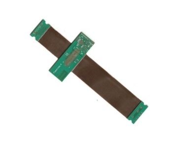
- 16 layer Flexible PCB
- 16 layer FR4 PCB
- 16 layer Rigid PCB
- 16 layer Rigid-flex PCB
- 16 layer HDI PCB

Rigid PCB
What Are the Applications of 16 Layer PCB?
There are lots of applications of 16 layer PCBs. Because of the lightweight and small size, we can employ this PCB in many applications. As well, you get a lot of connections space on this circuit board.

16 Layer PCB Applications
For building machines for the aerospace industry, these PCBs are much utilized. We use this printed circuit board to manufacture devices in sectors requiring crosstalk levels. Some other main applications of 16 layer circuit boards are as follows.
- Communication systems
- Computer systems
- Satellite systems
- Fire alarm systems
- Fire alarm systems
- Nuclear detector systems
- Laboratory test equipment
- Industrial control
- Repeater of cell phone
- Medical equipment (CAT scan, X-ray)
- Positioning and tracking network for GPS technology
- Atomic accelerators
- Equipment of space probe
- Weather analysis system
What Are the Advantages of a 16 Layer PCB?
There are numerous advantages of 16 layer circuit boards. Because of its various benefits, the use of this circuit board is gaining popularity. Its technical properties gives it an advantage as the best circuit board you can work with. This is especially true for high-density applications with high speed needs.

16 Layer PCB Advantages
The main advantages you get from 16 layer PCB are as follows:
- Great quality
- Lightweight
- Small size
- Great durability
- Superbly powerful
How to Design a 16-Layer PCB?
The designing process for a 16-layer PCB is quite critical. As the whole product output depends on the design of the PCB, the designer should be very careful as any minor mistake can incur a loss. As you proceed with the manufacturing process on the base of the design, you can not go back to change anything.

16-layer Stack-Up
You can use the help of many designing software to design any 16 layer circuit board. You should put every little detail here to get the most accurate design. The more precise your design is, the more accurate the PCB will turn out to be.
You need to consider the manufacturing process while designing the printed circuit board. The designer, manufacturer, and the consumer should communicate well during the process. Watch the following video to gather more insights about PCB design.
What Is the Manufacturing Process of 16 Layer PCB?
The manufacturing process of 16 layer PCB is complicated. The manufacturer should pay prudent attention to the operation, or all operations go in vain. The circumstances will bring money loss as well.
You need to maintain a solid idea of the 16 layer board design you have on mind. You should have specific production factors, remember where you placed the components, and etc. You also should pay special attention to significant circumstances while the manufacturing process is undergoing.

Manufacturing Process of a 16 Layer PCB
The manufacturing process of 16 layer PCB contains the following methods:
- Design schematic
- PCB stackup
- Vias
- Signal integrity
- Power integrity
- Breakdown pattern
Watch the following video to know more about multilayer circuit boards.
How Do You Position Ground Plane & Power Plane in 16 Layer PCB?
The ground plane and power planes are very crucial for 16 layer PCBs. They operate to connect the circuits to the ground. The power plane and ground plane as well as spread the required power among the PCB components.
You can work with specific calculations to place the ground planes and power planes on the 16 layer PCB. The analysis will provide you with the proper guideline for spacing the planes. You will have a clear idea of where one should be placed.
Proper positioning of the power and ground planes is very effective for PCB efficiency. With this calculation, you will get suitable locations by positioning the components on the board. They all go in different positions.
How Do You Place the Routing & Keep Out Layers on 16 Layer PCB?
There are some specific rules to place the routing and keep out layers on 16 layer PCB. Placing them right will make the PCB more efficient, so the board will not fail during the functioning process. You clearly need to have a comprehensive understanding of PCB routing.
You should be very careful while following these rules of placement. A minor glitch in these layers can cause considerable constraints.

Routing in 16 Layer PCB
Routing layers connect all the components on the 16 layer PCB. So, you have to place the routing layers between the internal layers of the PCB. Again, proper placement of these layers (lower and upper surface) generates optimum performance result.
It is essential to manage adequate spacing for ground planes. There should be enough protection for the traces on the board so that the PCB traces endure an extended period of use.
How Do You Compare 16 Layer PCB to 14 Layer PCB?
A 14 layer PCB is a printed circuit board with 14 layers. You can guess the compatibility between 14 layer PCB and 16 layer PCB based on their names. The 16 layer printed board has two more layers than the 14 one.

14 Layer PCB
Because of the additional two layers on the 16 layer board, the 16 layer board usually tends to perform better than the 14 layer board. For this reason, 16 layer boards are used in more high-speed and high-density applications. The 16 layer PCB gets preference from discerning customers.
The extra two layers also decrease signal impedance on 16 layers printed board than the 14 layer PCB. You can say that the 14 layer PCB possesses higher signal impedance than 16 layers one.
The additive two-layer as well provides more space for placing the components on the 16 layer board. There is more surface area on a 16 layer board. You can put up more efficient components on those two extra layers.
If you consider the current conduction capacity, 16 layer circuit boards provide better performance than a 14 layer PCB even if their designs are compatible with higher current loads. That’s why there is a lower possibility of overloading in 16 layer circuit board applications.
How Can You Protect the Traces on 16 Layer PCB?
You must protect the PCB traces to prevent damage and promote the longevity of a 16 layer PCB board. By selecting the location of the traces, you can easily save them from damages.
Making the location of the traces is the best way to keep them safe. You can utilize a solder mask for this purpose.

Traces on 16 Layer PCB
The marked locations help the developers to find the blueprints. Then, they can ignore the places with traces. Thus the PCB traces are kept safe.
What Are the Storage Conditions for 16 Layer PCB?
Storage condition is one of the main concerns of 16 layer PCB. For keeping the best condition of the storage, we need to keep it dry. And to keep it dry, we should keep our printed circuit board away from any moisture or water.
Keeping the circuit board close to any moisture or water will cause delamination. It is essential to keep the circuit board in a dry and cool environment.

Storage Condition for 16 Layer PCB
The 16 layer circuit board should be put into moisture barrier bags to prevent delamination from moisture. The moisture barrier bags play a crucial role in resisting the PCB’s moisture.
Again, using a humidity indicator card is a good idea to lower moisture absorption. You can also consider using desiccant bags for this purpose. These additional tools can help control the moisture amount.
Is 16 Layer PCB Weather Resistant?
Weather does not have any effect on the functionality of the 16 layer PCB. You can use this PCB in any sort of weather condition.

High Density 16 Layer PCB
You can even use the printed circuit board in rainy weather without any chance of damaging it. There is no risk of damage even in the rain, which is actually great.
The water absorption rate of 16 layer PCB is very low. And so, we can logically say that the 16 layer PCB is somewhat resistant to water.
The PCB is also UV ray resistant, making them usable in the sun and any sunny weather. To sum up, we can say that a 16 layer board is weather-resistant and can be used in any condition.
What Are the Limitations of a 16 Layer PCB?
Though we get a lot of benefits from 16 layer PCB, this PCB has some limitations as well.

Limitations of a 16 Layer PCB
There are only a few limitations that the 16 layer circuit board has. Some of its notable disadvantages include:
Complicated Manufacturing Process
As you spend a lot of money on the manufacturing process of the 16 layer circuit board, it’s expected that the manufacturing process is very complicated. The production process takes a lot of steps.
As there are a significant number of layers on the board, the layering process is sophisticated. This means time requirements on the manufacturer’s end. The PCB fabricator also needs to be careful with all the small details.
High Production Cost
A 16 layer PCB requires a hefty amount of money for the manufacturing process. The price is high compared to other PCB production costs.
A 16 layer circuit board requires advanced machines and PCB materials to produce. This board needs dedicated human resources to make. All in all, these costs so add up.
Longer Manufacturing Time
The manufacturing process of a 16 layer board takes a considerable amount of time. As the production process is complicated, you need to have some patience for the production process to be finalized.
As the circuit board requires unique materials and machines, sometimes the manufacturer needs time to arrange all the elements together. Logistics and supply chain demands can also add to the lead time needed.
Supply Limitation
Generally, the PCB manufacturer may have a limited supply of 16 layer PCBs. Because of the significant production time, manufacturing cost, and other factors in the manufacturing process. Not all PCB manufacturers are competent enough to build these 16 layer PCBs. So, actually, this product is not quickly available on hand.
How Do You Test a 16 Layer PCB?
There are serious consequences if your 16 layer PCB fails to work. You need to be careful that your PCB does not fail. Of course, you don’t want a negative outcome, so you need to take precautionary steps.

Testing 16 Layer PCB
You should test your 16 layer board multiple times to avoid these issues. Make sure that your PCB operates fine before you put it up for use in applications. There are some testing techniques that you can follow for testing the functionality of your 16 layer board which are as follows:
- Flying Probe Test (FPT)
- Automated optical inspection (AOI test)
- In-circuit testing method
- Automated X-ray Inspection (AXI)
How to Choose the Right Manufacturer of 16 Layer PCB?
Choosing the appropriate manufacturer for your 16 layer PCB is very important. Selecting the wrong manufacturer can lead your project to complete disaster and loss. You can choose the right manufacturer if you follow some steps such as:
- The manufacturer should have enough knowledge of PCBs.
- It would be great if the manufacturer worked with your type of project before.
- The manufacturer should employ PCB expert engineers.
- Manufacturing experience is a very important fact to check.
- You should be able to communicate clearly and quickly with the manufacturer.
- The manufacturing company should have certificates for their products.
- If possible, pay a visit to the area of the manufacturing company and see if everything checks out.
Conclusion
The efficiency 16 layer PCB is unquestionable. An excellent opportunity awaits if you use the best 16 layer board to fulfill your project requirements. With a great manufacturer, you can also customize your 16 layer board.
SMTFAB can accommodate all your 16 layer PCB needs. Your project is safe with us.
If you want to talk to us about our services or learn more about these PCBs, you are always welcome to contact us. We are here at your service.
Proficient Fabricator of 16 Layer PCB in China
Above everything else, your PCB manufacturer needs to be dependable. We are SMTFAB, a PCB supplier with a broad range of experience in the field. We make 16 Layer PCBs that you can trust.
- Over 3000+ international customers
- OEM PCB maker
- Provide turn-key solutions for your business
- Complete range of PCB testing and inspection
- Deliver to your doorstep on time
Just the Right 16 Layer PCB for You
You don’t want PCBs that are great in quality but are very expensive. You want a 16 Layer PCB with great quality as well as a great price. This is why you need us, SMTFAB.
SMTFAB offers distinguished PCB assembly and fabrication services to suit your requirements. The 16 Layer PCB we will deliver to you will adequately fix your industrial or personal PCB requirements.
Don’t waste time looking for the second-best, SMTFAB is your best option.
Types of 16 Layer PCBSuited for Your Business
To gain the advantages of both Rigid PCB and Flex PCB, you can order a 16 Layer Rigid-flex PCB. Our plant makes Flex Connector PCBs that have sufficient strength and pliability.
With the use of FR4, PCBs are able to be mass-produced quickly. SMTFAB can give you a fast PCB for your 16 Layer FR4 PCB bulk order. FR4 is standard PCB substrate material.
Our 16 Layer ENIG PCB can be costlier than Aluminum PCBs or FR4 PCBs. However, the advantages are worth mentioning. Mainly, ENIG does not need electroplating.
If you require a High-frequency PCB, then consider having a 16 Layer Thick Copper PCB built. These boards are used for heavy-duty industrial applications, which are typical for digital communication processes.
For customers who need a high density of connection pads, 16 Layer HDI PCB is a sound choice. Increasing sales of smartphones, IoT, laptops, and drones have increased demand for this board.
High TG PCBs are part of our specialized products. Hence, we can give you 16 Layer High TG PCB using advanced materials such as Rogers, NanYa, or Isola. The temperature tolerated is 180°C. The planar surface is flat.
SMTFAB – The Excellent 16 Layer PCB Supplier
We want you to know our capacity as a competent 16 Layer PCB manufacturer. For this reason, we are featuring this short video. In it, we show the orderly facilities we have, as well as our professional crew.
SMTFAB only follows strict and safe manufacturing processes for 16 Layer PCBs. As this is so, we can say confidently that our products are defect-free.
Our PCBs are built to last and make you fully satisfied.
Related 16 Layer PCB
16 Layer PCB Production Details As Following Up
- Production Facility
- PCB Capabilities
- PCB Materials
- Shipping Methods
- Payment Methods
- Send Us Inquiry
| Item | Capability |
| Layer Count | 1-40layers |
| Base Material | KB、Shengyi、ShengyiSF305、FR408、FR408HR、IS410、FR406、GETEK、370HR、IT180A、Rogers4350B、Rogers4000、PTFE Laminates(Rogers series、Taconic series、Arlon series、Nelco series)、Rogers/Taconic/Arlon/Nelco laminate with FR-4 material(including partial Ro4350B hybrid laminating with FR-4) |
| Board Type | Backplane、HDI、High multi-layer 、blind&buried PCB、Embedded Capacitance、Embedded resistance board 、Heavy copper power PCB、Backdrill. |
| Board Thickness | 0.2-5.0mm |
| Copper Thickness | Min. 1/2 OZ, Max. 10 OZ |
| PTH Wall | 25um(1mil) |
| Maximum Board Size | 1100*500mm(43”*19”) |
| Min laser drilling size | 4mil |
| Min. Spacing/Tracing | 2.7mil/2.7mil |
| Solder Mask | Green, Black, Blue, Red, White, Yellow,Purple matte/glossy |
| Surface Treatment | Flash gold(electroplated gold)、ENIG、Hard gold、Flash gold、HASL Lead free、OSP、ENEPIG、Soft gold、Immersion silver、Immersion Tin、ENIG+OSP,ENIG+Gold finger,Flash gold(electroplated gold)+Gold finger,Immersion silver+Gold finger,Immersion Tin+Gold finger. |
| Min. Annular Ring | 3mil |
| Aspect ratio | 10:1(HASL Lead free、HASL Lead、ENIG、Immersion Tin、Immersion silver、ENEPIG);8:1(OSP) |
| Impedance control | ±5ohm(<50ohm), ±10%(≥50ohm) |
| Other Techniques | Blind/Buried Via |
| Gold Fingers | |
| Press Fit | |
| Via in Pad | |
| Electrical Test |
Here there’re many laminate material datasheets, they’re useful and helpful for you, please see them:
| SUPPLIER | PCB LAMINATE | TYPE | MATERIAL DATASHEET | TG | TD | DK(1MHZ) | DK(1GHZ) | DK(10GHZ) |
| KB | KB-6160 | FR4 | DOWNLOAD | 135 | 305 | 4.35 | – | – |
| KB-6160A | FR4 | DOWNLOAD | 135 | 305 | 4.35 | – | – | |
| KB-6160C | FR4 | DOWNLOAD | 135 | 314 | 4.7 | – | – | |
| KB-6150 KB-6150C | FR4 | DOWNLOAD | 132 | 305 | 4.6 | – | – | |
| KB-6164 | FR4 | DOWNLOAD | 142 | 330 | 4.8 | – | – | |
| KB-6164F | FR4 | DOWNLOAD | 145 | 340 | 4.8 | – | – | |
| KB-6165F | FR4 | DOWNLOAD | 150 | 346 | 4.8 | – | – | |
| KB-6167F | FR4 | DOWNLOAD | 170 | 349 | 4.8 | – | – | |
| SHENGYI | S1141 | FR4 | DOWNLOAD | 135 | 310 | 4.6 | – | – |
| S1141KF | FR4 | DOWNLOAD | 140 | 350 | 4.7 | – | – | |
| S1000 | FR4 | DOWNLOAD | 155 | 335 | 4.9 | – | – | |
| S1170 | FR4 | DOWNLOAD | 170 | 335 | 4.6 | – | – | |
| S1000-2 | FR4 | DOWNLOAD | 170 | 335 | 4.8 | – | – | |
| S1155 | FR4 | DOWNLOAD | 135 | 370 | 4.7 | – | – | |
| ITEQ | IT-158 | FR4 | DOWNLOAD | 150 | 340 | 4.6-4.8 | – | – |
| IT-180 | FR4 | DOWNLOAD | 180 | 350 | 4.5-4.7 | – | – | |
| TUC | TU-768 | FR4 | DOWNLOAD | 180 | 350 | – | 4.3-4.4 | 4.3 |
| TU-872 | Modified Epoxy | DOWNLOAD | 200 | 340 | – | 3.8-4.0 | 3.8 | |
| ROGERS | RO 3003 | Cer/PTFE | DOWNLOAD | – | 500 | – | – | 3 |
| RO 3010 | Cer/PTFE | DOWNLOAD | – | 500 | – | – | 10.2 | |
| RO 4003 | Hydrocarbon/Cer | DOWNLOAD | >280 | 425 | – | – | 3.38 | |
| RO 4350B | Hydrocarbon/Cer | DOWNLOAD | >280 | 390 | – | – | 3.48 | |
| RT/duroid 5880 | PTFE/Glass | DOWNLOAD | – | 500 | – | – | 2.2 | |
| ISOLA | Polyclad 370HR | FR4 | DOWNLOAD | 170 | 340 | 4.8-5.1 | – | – |
| FR406-HR | FR4 | DOWNLOAD | 190 | 325 | 3.91 | 3.86 | 3.81 | |
| FR408-HR | FR4 | DOWNLOAD | 200 | 360 | 3.72 | 3.69 | 3.65 | |
| P96 | Polyimide | DOWNLOAD | 260 | 416 | – | 3.78 | 3.73 | |
| Hitachi | MCL-BE- 67G | Modified Epoxy | DOWNLOAD | 140 | 340 | 4.9 | 4.4 | – |
| MCL-E-679F | FR4 | DOWNLOAD | 170 | 350 | 4.2-4.4 | 4.3-4.5 | – | |
| MCL-LX-67Y | Special Laminate | DOWNLOAD | 185-195 | 325-345 | – | 3.4-3.6 | – | |
| Nelco | N4000-13 | Modified Epoxy | DOWNLOAD | 210-240 | 365 | – | 3.7 | 3.6 |
| N4000-13EP | Modified Epoxy | DOWNLOAD | 210-240 | 350 | – | 3.4 | 3.2 | |
| N4000-13SI | Modified Epoxy | DOWNLOAD | 210-240 | 350 | – | 3.4 | 3.2 | |
| N4000-13EP SI | Modified Epoxy | DOWNLOAD | 210-240 | 350 | – | 3.4 | 3.2 | |
| Taconic | TLX-6 | PTFE | DOWNLOAD | – | – | – | – | 2.65 |
| TLX-7 | PTFE | DOWNLOAD | – | – | – | – | 2.6 | |
| TLX-8 | PTFE | DOWNLOAD | – | – | – | – | 2.55 | |
| TLX-9 | PTFE | DOWNLOAD | – | – | – | – | 2.45 | |
| RF35 | PTFE | DOWNLOAD | <315 | – | 3.5 | – | 3.5 | |
| TLC-27 | PTFE | DOWNLOAD | – | – | – | – | 2.75 | |
| TLC-30 | PTFE | DOWNLOAD | – | – | – | – | 3 | |
| TLC-32 | PTFE | DOWNLOAD | – | – | – | – | 3.2 | |
| Arlon | Arlon 25N | Cer | DOWNLOAD | 260 | – | – | – | 3.38 |
| Arlon 25FR | Cer | DOWNLOAD | 260 | – | – | – | 3.58 | |
| Arlon 33N | Polymide | DOWNLOAD | >250 | 353 | 4 | – | – | |
| Arlon 35N | Polymide | DOWNLOAD | >250 | 363 | 4.2 | – | – | |
| Arlon 85N | Polymide | DOWNLOAD | 250 | 387 | 4.2 | – | – | |
| Stablcor | ST325 | – | DOWNLOAD | Thermal conductivity:75w/m.k(with 1oz copper) | ||||
| ST10 | – | DOWNLOAD | Thermal conductivity:325w/m.k(with 1oz copper) | |||||
| Panasonic | R-1566W | FR4 | DOWNLOAD | 140 | 330 | 4.95 | 4.7 | 4.65 |
| Ventec | VT-901 | Polymide | DOWNLOAD | 250 | 390 | 4.2-4.5 | 4.0-4.3 | – |
| VT-90H | Polymide | DOWNLOAD | 250 | 390 | 4.2-4.5 | 4.0-4.3 | – | |
| Bergquist | ht-04503 | – | DOWNLOAD | Thermal conductivity:2.2w/m.k(with 1oz copper) | ||||
Delivery
SMTFAB offers flexible shipping methods for our customers, you may choose from one of the methods below.
1. DHL
DHL offers international express services in over 220 countries.
DHL partners with SMTFAB and offers very competitive rates to customers of SMTFAB.
It normally takes 3-7 business days for the package to be delivered around the world.
2. UPS
UPS gets the facts and figures about the world’s largest package delivery company and one of the leading global providers of specialized transportation and logistics services.
It normally takes 3-7 business days to deliver a package to most of the addresses in the world.
3. TNT
TNT has 56,000 employees in 61 countries.
It takes 4-9 business days to deliver the packages to the hands
of our customers.
4. FedEx
FedEx offers delivery solutions for customers around the world.
It takes 4-7 business days to deliver the packages to the hands
of our customers.
5. Air, Sea/Air, and Sea
If your order is of large volume with SMTFAB, you can also choose
to ship via air, sea/air combined, and sea when necessary.
Please contact your sales representative for shipping solutions.
Note: if you need others, please contact your sales representative for shipping solutions.
On our website you can use the following payment methods:
Telegraphic Transfer(TT): A telegraphic transfer (TT) is an electronic method of transferring funds utilized primarily for overseas wire transactions. It’s very convenient to transfer.
Bank/Wire transfer: To pay by wire transfer using your bank account, you need to visit your nearest bank branch with the wire transfer information. Your payment will be completed 3-5 business days after you have finished the money transfer.
Paypal: Pay easily, fast and secure with PayPal. many other credit and debit cards via PayPal.
Credit Card: You can pay with credit card: Visa, Visa Electron, MasterCard, Maestro.
[contact-form-7 id=”764″ title=”Quick Quote”]
Incomparable 16 Layer PCB Made by SMTFAB
SMTFAB is a champion PCB fabricator in China. We set up business in 2008, and since then, we have been making excellent Multilayer PCBs for international and domestic clients. Your 16 Layer PCB is guaranteed to be high-class.
- Proactive prevention of flaws by superb multilayer stack-up design
- Use symmetrical PCB design to reduce warps
- PCB multilayers cool uniformly, which makes the product durable
- Accurate usage of PCB space to fit SMT components
- Lightweight and multifunctional, for your many gadget constraints
Our premium 16 Layer PCB makes use of advanced PCB fabrication processes. Since we conform to ISO 9000 and ISO 1400, we are dually watchful of Quality Control and Environmental Management Systems. Part of our company credo is to take care of you as a customer to guarantee your contentment. In addition, we use the safest practices in PCB manufacture.
For your 16 Layer PCB, you can work hand-in-hand with our senior engineering staff. For instance, if you need help with the circuit board design, we are just an email or call away. If you need a complicated, custom-made PCB, for example, an extra Long PCB, we can assist with that too.
If your query is more specific, we can go the extra mile. For example, you can request a COC (Certificate of Conformity) report for your 16 Layer PCB order. Another request we will gladly accommodate is a soldering sample. Anything you need, you can ask our approachable customer support team.
We train our salespersons well, and they are available 24/7 for you.
You see, SMTFAB is an esteemed 16 Layer PCB maker that you can trust. Inquire from us now!
16 Layer PCB| The Ultimate FAQ Guide
16 layer PCB is very popular for its demand in high density and high-speed applications. The modern world requires faster electronic appliances, so the demand for 16 layer PCB is on the rise. Many applications nowadays use this type of PCB for better performance.
SMTFAB is one of the leading PCB manufacturing companies situated in China. We produce the best quality 16 layer PCB, which is remarkably efficient and durable. More than 60 countries worldwide get their 16 layer PCBs from us.
If you want to know in detail about this 16 layer printed circuit board, you can take a look at this FAQ guide. This ultimate FAQ guide contains almost everything about this PCB.
- What Is 16 Layer PCB?
- What Are the Materials of 16 Layer PCB?
- What Are the Components of 16 Layer PCB?
- How to Compare Between a Single Layer PCB and a 16 Layer PCB?
- What Types of PCBs Can You Make with a 16 Layer PCB?
- What Are the Applications of 16 Layer PCB?
- What Are the Advantages of a 16 Layer PCB?
- How to Design a 16 Layer PCB?
- What Is the Manufacturing Process of 16 Layer PCB?
- How Do You Position Ground Plane & Power Plane in 16 Layer PCB?
- How Do You Place the Routing & Keep Out Layers on 16 Layer PCB?
- How Do You Compare 16 Layer PCB to 14 Layer PCB?
- How Can You Protect the Traces on 16 Layer PCB?
- What Are the Storage Conditions for 16 Layer PCB?
- Is 16 Layer PCB Weather Resistant?
- What Are the Limitations of a 16 Layer PCB?
- How Do You Test a 16 Layer PCB?
- How to Choose the Right Manufacturer of 16 Layer PCB?
What Is 16 Layer PCB?
A 16 layer PCB is a multilayer printed circuit board with 16 layers. Ten layers among the 16 are routing layers, and the rest are other types of layers. The 16 layer PCB is one of the most efficient circuit boards.
16 Layer PCB
A 16 layer PCB is used in high-density applications. Applications that need high speed for functioning use these PCBs. You can say a 16 layer printed circuit board is the best among all circuit boards.
What Are the Materials of 16 Layer PCB?
A 16 layer PCB usually contains numerous layers. We need to fabricate and laminate each layer to get the perfect 16 layer board. Several PCB materials are used in layers on a 16 layer board.
16 Layer PCB Materials
Some significant materials used from top to bottom of the 16 layers printed board are as follows:
- Substrate materials
- Soldermask
- Copper materials
- Silkscreen materials
Substrate materials work as the base of the printed circuit board. The substrate materials are glass epoxy materials. There are both cheap and costly options for substrate materials.
The copper layer is essential in the PCB layers as well. Copper here functions as a conductive material. Usually, the copper layer is pretty thin.
What Are the Components of 16 Layer PCB?
Obviously, there are 16 layers in 16 layer printed circuit boards. All of these layers come in several dimensions with several functionalities. All of these layers make up with the components of the circuit board.
The routing layer number is 10 in the 16 layers PCB. The rest 6 are for different reasons. The various components are combined in the board to provide the best results possible as you employ the board in other applications.
16 Layer PCB Components
The main components aid the functionality of this 16 layer board and its applications. The main components of a 16 layer PCB are as follows:
Prepreg Sheets
There are several layers of prepreg material on a 16 layer board. These layers form the materials of insulation on the board.
These sheets are the woven cloth of fiberglass. They are coated with a resin system. There are also varieties of design available for prepreg.
Copper Foil Sheets
The copper foil sheets are vital for 16 layer PCB. The outer layer of the circuit board is made with these copper foil sheets.
The sheets work as the primary conductive materials for this printed circuit board. The sheets of copper foil transmit signals and power through the board as the conductive material.
Laminate Sheets
These sheets of laminates are made with glass or resin material. The material also has a copper layer on each side. These copper layers hold the glass laminates bonding.
The signal layers and inner plane are etched on the laminate pieces. Thus they all become part of the components.
How to Compare Between a Single Layer PCB and a 16 Layer PCB?
A Single-layer PCB and a 16 layer PCB have some fundamental differences. It is essential to know the comparison between these two to optimize your application in multilayer PCB projects.
These circuit boards are primarily different in terms of layer count. A 16 layer PCB is a classic representative of a multilayer printed circuit board because it offers impactful electronic application features compared to a Single-layer PCB.
Single Layer PCB
Single-layer circuit boards have space constraints because of the single layer count. But there is massive space on 16 layer boards. So, you can use this multilayered board to deal with compact designs, as well, you can place all your components. As a 16 layer circuit board has more layers and more elements on it, it performs better than a single-layer one. It is more efficient as well.
The single-layer printed circuit board contains a significant signal impedance, limiting its execution. On the contrary, a 16 layer printed circuit board possesses very low impedance, which allows it to perform much better.
There is a considerable difference in cost between these two PCBs. A 16 layer circuit board costs a lot at the manufacturing process due to its much layer count. But the single-layer one doesn’t cost as much as it has only one layer.
A single-layer circuit board is used in more simple applications. But a 16 layer circuit board is used for applications that needs compatibility with other high-functioning devices.
Another issue: multilayer circuit boards support carrying high current loads in high-frequency applications. A 16 layer PCB also delivers superb performance in current conduction. On the contrary, you can’t rely on a single-layer PCB to transfer high currents.
What Types of PCBs Can You Make with a 16 Layer PCB?
If there is a requirement for a multilayer PCB, you can decide on using a 16 layer circuit board. This layer count is applicable to all types of circuit board designs.
With a 16 layer printed circuit board, you can manufacture the following types of printed board. All of these boards are highly functional.
- 16 layer Flexible PCB
- 16 layer FR4 PCB
- 16 layer Rigid PCB
- 16 layer Rigid-flex PCB
- 16 layer HDI PCB
Rigid PCB
What Are the Applications of 16 Layer PCB?
There are lots of applications of 16 layer PCBs. Because of the lightweight and small size, we can employ this PCB in many applications. As well, you get a lot of connections space on this circuit board.
16 Layer PCB Applications
For building machines for the aerospace industry, these PCBs are much utilized. We use this printed circuit board to manufacture devices in sectors requiring crosstalk levels. Some other main applications of 16 layer circuit boards are as follows.
- Communication systems
- Computer systems
- Satellite systems
- Fire alarm systems
- Fire alarm systems
- Nuclear detector systems
- Laboratory test equipment
- Industrial control
- Repeater of cell phone
- Medical equipment (CAT scan, X-ray)
- Positioning and tracking network for GPS technology
- Atomic accelerators
- Equipment of space probe
- Weather analysis system
What Are the Advantages of a 16 Layer PCB?
There are numerous advantages of 16 layer circuit boards. Because of its various benefits, the use of this circuit board is gaining popularity. Its technical properties gives it an advantage as the best circuit board you can work with. This is especially true for high-density applications with high speed needs.
16 Layer PCB Advantages
The main advantages you get from 16 layer PCB are as follows:
- Great quality
- Lightweight
- Small size
- Great durability
- Superbly powerful
How to Design a 16-Layer PCB?
The designing process for a 16-layer PCB is quite critical. As the whole product output depends on the design of the PCB, the designer should be very careful as any minor mistake can incur a loss. As you proceed with the manufacturing process on the base of the design, you can not go back to change anything.
16-layer Stack-Up
You can use the help of many designing software to design any 16 layer circuit board. You should put every little detail here to get the most accurate design. The more precise your design is, the more accurate the PCB will turn out to be.
You need to consider the manufacturing process while designing the printed circuit board. The designer, manufacturer, and the consumer should communicate well during the process. Watch the following video to gather more insights about PCB design.
What Is the Manufacturing Process of 16 Layer PCB?
The manufacturing process of 16 layer PCB is complicated. The manufacturer should pay prudent attention to the operation, or all operations go in vain. The circumstances will bring money loss as well.
You need to maintain a solid idea of the 16 layer board design you have on mind. You should have specific production factors, remember where you placed the components, and etc. You also should pay special attention to significant circumstances while the manufacturing process is undergoing.
Manufacturing Process of a 16 Layer PCB
The manufacturing process of 16 layer PCB contains the following methods:
- Design schematic
- PCB stackup
- Vias
- Signal integrity
- Power integrity
- Breakdown pattern
Watch the following video to know more about multilayer circuit boards.
How Do You Position Ground Plane & Power Plane in 16 Layer PCB?
The ground plane and power planes are very crucial for 16 layer PCBs. They operate to connect the circuits to the ground. The power plane and ground plane as well as spread the required power among the PCB components.
You can work with specific calculations to place the ground planes and power planes on the 16 layer PCB. The analysis will provide you with the proper guideline for spacing the planes. You will have a clear idea of where one should be placed.
Proper positioning of the power and ground planes is very effective for PCB efficiency. With this calculation, you will get suitable locations by positioning the components on the board. They all go in different positions.
How Do You Place the Routing & Keep Out Layers on 16 Layer PCB?
There are some specific rules to place the routing and keep out layers on 16 layer PCB. Placing them right will make the PCB more efficient, so the board will not fail during the functioning process. You clearly need to have a comprehensive understanding of PCB routing.
You should be very careful while following these rules of placement. A minor glitch in these layers can cause considerable constraints.
Routing in 16 Layer PCB
Routing layers connect all the components on the 16 layer PCB. So, you have to place the routing layers between the internal layers of the PCB. Again, proper placement of these layers (lower and upper surface) generates optimum performance result.
It is essential to manage adequate spacing for ground planes. There should be enough protection for the traces on the board so that the PCB traces endure an extended period of use.
How Do You Compare 16 Layer PCB to 14 Layer PCB?
A 14 layer PCB is a printed circuit board with 14 layers. You can guess the compatibility between 14 layer PCB and 16 layer PCB based on their names. The 16 layer printed board has two more layers than the 14 one.
14 Layer PCB
Because of the additional two layers on the 16 layer board, the 16 layer board usually tends to perform better than the 14 layer board. For this reason, 16 layer boards are used in more high-speed and high-density applications. The 16 layer PCB gets preference from discerning customers.
The extra two layers also decrease signal impedance on 16 layers printed board than the 14 layer PCB. You can say that the 14 layer PCB possesses higher signal impedance than 16 layers one.
The additive two-layer as well provides more space for placing the components on the 16 layer board. There is more surface area on a 16 layer board. You can put up more efficient components on those two extra layers.
If you consider the current conduction capacity, 16 layer circuit boards provide better performance than a 14 layer PCB even if their designs are compatible with higher current loads. That’s why there is a lower possibility of overloading in 16 layer circuit board applications.
How Can You Protect the Traces on 16 Layer PCB?
You must protect the PCB traces to prevent damage and promote the longevity of a 16 layer PCB board. By selecting the location of the traces, you can easily save them from damages.
Making the location of the traces is the best way to keep them safe. You can utilize a solder mask for this purpose.
Traces on 16 Layer PCB
The marked locations help the developers to find the blueprints. Then, they can ignore the places with traces. Thus the PCB traces are kept safe.
What Are the Storage Conditions for 16 Layer PCB?
Storage condition is one of the main concerns of 16 layer PCB. For keeping the best condition of the storage, we need to keep it dry. And to keep it dry, we should keep our printed circuit board away from any moisture or water.
Keeping the circuit board close to any moisture or water will cause delamination. It is essential to keep the circuit board in a dry and cool environment.
Storage Condition for 16 Layer PCB
The 16 layer circuit board should be put into moisture barrier bags to prevent delamination from moisture. The moisture barrier bags play a crucial role in resisting the PCB’s moisture.
Again, using a humidity indicator card is a good idea to lower moisture absorption. You can also consider using desiccant bags for this purpose. These additional tools can help control the moisture amount.
Is 16 Layer PCB Weather Resistant?
Weather does not have any effect on the functionality of the 16 layer PCB. You can use this PCB in any sort of weather condition.
High Density 16 Layer PCB
You can even use the printed circuit board in rainy weather without any chance of damaging it. There is no risk of damage even in the rain, which is actually great.
The water absorption rate of 16 layer PCB is very low. And so, we can logically say that the 16 layer PCB is somewhat resistant to water.
The PCB is also UV ray resistant, making them usable in the sun and any sunny weather. To sum up, we can say that a 16 layer board is weather-resistant and can be used in any condition.
What Are the Limitations of a 16 Layer PCB?
Though we get a lot of benefits from 16 layer PCB, this PCB has some limitations as well.
Limitations of a 16 Layer PCB
There are only a few limitations that the 16 layer circuit board has. Some of its notable disadvantages include:
Complicated Manufacturing Process
As you spend a lot of money on the manufacturing process of the 16 layer circuit board, it’s expected that the manufacturing process is very complicated. The production process takes a lot of steps.
As there are a significant number of layers on the board, the layering process is sophisticated. This means time requirements on the manufacturer’s end. The PCB fabricator also needs to be careful with all the small details.
High Production Cost
A 16 layer PCB requires a hefty amount of money for the manufacturing process. The price is high compared to other PCB production costs.
A 16 layer circuit board requires advanced machines and PCB materials to produce. This board needs dedicated human resources to make. All in all, these costs so add up.
Longer Manufacturing Time
The manufacturing process of a 16 layer board takes a considerable amount of time. As the production process is complicated, you need to have some patience for the production process to be finalized.
As the circuit board requires unique materials and machines, sometimes the manufacturer needs time to arrange all the elements together. Logistics and supply chain demands can also add to the lead time needed.
Supply Limitation
Generally, the PCB manufacturer may have a limited supply of 16 layer PCBs. Because of the significant production time, manufacturing cost, and other factors in the manufacturing process. Not all PCB manufacturers are competent enough to build these 16 layer PCBs. So, actually, this product is not quickly available on hand.
How Do You Test a 16 Layer PCB?
There are serious consequences if your 16 layer PCB fails to work. You need to be careful that your PCB does not fail. Of course, you don’t want a negative outcome, so you need to take precautionary steps.
Testing 16 Layer PCB
You should test your 16 layer board multiple times to avoid these issues. Make sure that your PCB operates fine before you put it up for use in applications. There are some testing techniques that you can follow for testing the functionality of your 16 layer board which are as follows:
- Flying Probe Test (FPT)
- Automated optical inspection (AOI test)
- In-circuit testing method
- Automated X-ray Inspection (AXI)
How to Choose the Right Manufacturer of 16 Layer PCB?
Choosing the appropriate manufacturer for your 16 layer PCB is very important. Selecting the wrong manufacturer can lead your project to complete disaster and loss. You can choose the right manufacturer if you follow some steps such as:
- The manufacturer should have enough knowledge of PCBs.
- It would be great if the manufacturer worked with your type of project before.
- The manufacturer should employ PCB expert engineers.
- Manufacturing experience is a very important fact to check.
- You should be able to communicate clearly and quickly with the manufacturer.
- The manufacturing company should have certificates for their products.
- If possible, pay a visit to the area of the manufacturing company and see if everything checks out.
Conclusion
The efficiency 16 layer PCB is unquestionable. An excellent opportunity awaits if you use the best 16 layer board to fulfill your project requirements. With a great manufacturer, you can also customize your 16 layer board.
SMTFAB can accommodate all your 16 layer PCB needs. Your project is safe with us.
If you want to talk to us about our services or learn more about these PCBs, you are always welcome to contact us. We are here at your service.
Proficient Fabricator of 16 Layer PCB in China
Above everything else, your PCB manufacturer needs to be dependable. We are SMTFAB, a PCB supplier with a broad range of experience in the field. We make 16 Layer PCBs that you can trust.
- Over 3000+ international customers
- OEM PCB maker
- Provide turn-key solutions for your business
- Complete range of PCB testing and inspection
- Deliver to your doorstep on time
Just the Right 16 Layer PCB for You
You don’t want PCBs that are great in quality but are very expensive. You want a 16 Layer PCB with great quality as well as a great price. This is why you need us, SMTFAB.
SMTFAB offers distinguished PCB assembly and fabrication services to suit your requirements. The 16 Layer PCB we will deliver to you will adequately fix your industrial or personal PCB requirements.
Don’t waste time looking for the second-best, SMTFAB is your best option.
Types of 16 Layer PCBSuited for Your Business
To gain the advantages of both Rigid PCB and Flex PCB, you can order a 16 Layer Rigid-flex PCB. Our plant makes Flex Connector PCBs that have sufficient strength and pliability.
With the use of FR4, PCBs are able to be mass-produced quickly. SMTFAB can give you a fast PCB for your 16 Layer FR4 PCB bulk order. FR4 is standard PCB substrate material.
Our 16 Layer ENIG PCB can be costlier than Aluminum PCBs or FR4 PCBs. However, the advantages are worth mentioning. Mainly, ENIG does not need electroplating.
If you require a High-frequency PCB, then consider having a 16 Layer Thick Copper PCB built. These boards are used for heavy-duty industrial applications, which are typical for digital communication processes.
For customers who need a high density of connection pads, 16 Layer HDI PCB is a sound choice. Increasing sales of smartphones, IoT, laptops, and drones have increased demand for this board.
High TG PCBs are part of our specialized products. Hence, we can give you 16 Layer High TG PCB using advanced materials such as Rogers, NanYa, or Isola. The temperature tolerated is 180°C. The planar surface is flat.
Types of 16 Layer PCBSuited for Your Business
Types of 16 Layer PCBSuited for Your Business
To gain the advantages of both Rigid PCB and Flex PCB, you can order a 16 Layer Rigid-flex PCB. Our plant makes Flex Connector PCBs that have sufficient strength and pliability.
To gain the advantages of both Rigid PCB and Flex PCB, you can order a 16 Layer Rigid-flex PCB. Our plant makes Flex Connector PCBs that have sufficient strength and pliability.
To gain the advantages of both Rigid PCB and Flex PCB, you can order a 16 Layer Rigid-flex PCB. Our plant makes Flex Connector PCBs that have sufficient strength and pliability.
To gain the advantages of both Rigid PCB and Flex PCB, you can order a 16 Layer Rigid-flex PCB. Our plant makes Flex Connector PCBs that have sufficient strength and pliability.
With the use of FR4, PCBs are able to be mass-produced quickly. SMTFAB can give you a fast PCB for your 16 Layer FR4 PCB bulk order. FR4 is standard PCB substrate material.
With the use of FR4, PCBs are able to be mass-produced quickly. SMTFAB can give you a fast PCB for your 16 Layer FR4 PCB bulk order. FR4 is standard PCB substrate material.
With the use of FR4, PCBs are able to be mass-produced quickly. SMTFAB can give you a fast PCB for your 16 Layer FR4 PCB bulk order. FR4 is standard PCB substrate material.
With the use of FR4, PCBs are able to be mass-produced quickly. SMTFAB can give you a fast PCB for your 16 Layer FR4 PCB bulk order. FR4 is standard PCB substrate material.
Our 16 Layer ENIG PCB can be costlier than Aluminum PCBs or FR4 PCBs. However, the advantages are worth mentioning. Mainly, ENIG does not need electroplating.
Our 16 Layer ENIG PCB can be costlier than Aluminum PCBs or FR4 PCBs. However, the advantages are worth mentioning. Mainly, ENIG does not need electroplating.
Our 16 Layer ENIG PCB can be costlier than Aluminum PCBs or FR4 PCBs. However, the advantages are worth mentioning. Mainly, ENIG does not need electroplating.
Our 16 Layer ENIG PCB can be costlier than Aluminum PCBs or FR4 PCBs. However, the advantages are worth mentioning. Mainly, ENIG does not need electroplating.
If you require a High-frequency PCB, then consider having a 16 Layer Thick Copper PCB built. These boards are used for heavy-duty industrial applications, which are typical for digital communication processes.
If you require a High-frequency PCB, then consider having a 16 Layer Thick Copper PCB built. These boards are used for heavy-duty industrial applications, which are typical for digital communication processes.
If you require a High-frequency PCB, then consider having a 16 Layer Thick Copper PCB built. These boards are used for heavy-duty industrial applications, which are typical for digital communication processes.
If you require a High-frequency PCB, then consider having a 16 Layer Thick Copper PCB built. These boards are used for heavy-duty industrial applications, which are typical for digital communication processes.
For customers who need a high density of connection pads, 16 Layer HDI PCB is a sound choice. Increasing sales of smartphones, IoT, laptops, and drones have increased demand for this board.
For customers who need a high density of connection pads, 16 Layer HDI PCB is a sound choice. Increasing sales of smartphones, IoT, laptops, and drones have increased demand for this board.
For customers who need a high density of connection pads, 16 Layer HDI PCB is a sound choice. Increasing sales of smartphones, IoT, laptops, and drones have increased demand for this board.
For customers who need a high density of connection pads, 16 Layer HDI PCB is a sound choice. Increasing sales of smartphones, IoT, laptops, and drones have increased demand for this board.
High TG PCBs are part of our specialized products. Hence, we can give you 16 Layer High TG PCB using advanced materials such as Rogers, NanYa, or Isola. The temperature tolerated is 180°C. The planar surface is flat.
High TG PCBs are part of our specialized products. Hence, we can give you 16 Layer High TG PCB using advanced materials such as Rogers, NanYa, or Isola. The temperature tolerated is 180°C. The planar surface is flat.
High TG PCBs are part of our specialized products. Hence, we can give you 16 Layer High TG PCB using advanced materials such as Rogers, NanYa, or Isola. The temperature tolerated is 180°C. The planar surface is flat.
High TG PCBs are part of our specialized products. Hence, we can give you 16 Layer High TG PCB using advanced materials such as Rogers, NanYa, or Isola. The temperature tolerated is 180°C. The planar surface is flat.
SMTFAB – The Excellent 16 Layer PCB Supplier
We want you to know our capacity as a competent 16 Layer PCB manufacturer. For this reason, we are featuring this short video. In it, we show the orderly facilities we have, as well as our professional crew.
SMTFAB only follows strict and safe manufacturing processes for 16 Layer PCBs. As this is so, we can say confidently that our products are defect-free.
Our PCBs are built to last and make you fully satisfied.
Related 16 Layer PCB
Related 16 Layer PCB
Related 16 Layer PCB
16 Layer PCB Production Details As Following Up
- Production Facility
- PCB Capabilities
- PCB Materials
- Shipping Methods
- Payment Methods
- Send Us Inquiry
| Item | Capability |
| Layer Count | 1-40layers |
| Base Material | KB、Shengyi、ShengyiSF305、FR408、FR408HR、IS410、FR406、GETEK、370HR、IT180A、Rogers4350B、Rogers4000、PTFE Laminates(Rogers series、Taconic series、Arlon series、Nelco series)、Rogers/Taconic/Arlon/Nelco laminate with FR-4 material(including partial Ro4350B hybrid laminating with FR-4) |
| Board Type | Backplane、HDI、High multi-layer 、blind&buried PCB、Embedded Capacitance、Embedded resistance board 、Heavy copper power PCB、Backdrill. |
| Board Thickness | 0.2-5.0mm |
| Copper Thickness | Min. 1/2 OZ, Max. 10 OZ |
| PTH Wall | 25um(1mil) |
| Maximum Board Size | 1100*500mm(43”*19”) |
| Min laser drilling size | 4mil |
| Min. Spacing/Tracing | 2.7mil/2.7mil |
| Solder Mask | Green, Black, Blue, Red, White, Yellow,Purple matte/glossy |
| Surface Treatment | Flash gold(electroplated gold)、ENIG、Hard gold、Flash gold、HASL Lead free、OSP、ENEPIG、Soft gold、Immersion silver、Immersion Tin、ENIG+OSP,ENIG+Gold finger,Flash gold(electroplated gold)+Gold finger,Immersion silver+Gold finger,Immersion Tin+Gold finger. |
| Min. Annular Ring | 3mil |
| Aspect ratio | 10:1(HASL Lead free、HASL Lead、ENIG、Immersion Tin、Immersion silver、ENEPIG);8:1(OSP) |
| Impedance control | ±5ohm(<50ohm), ±10%(≥50ohm) |
| Other Techniques | Blind/Buried Via |
| Gold Fingers | |
| Press Fit | |
| Via in Pad | |
| Electrical Test |
Here there’re many laminate material datasheets, they’re useful and helpful for you, please see them:
| SUPPLIER | PCB LAMINATE | TYPE | MATERIAL DATASHEET | TG | TD | DK(1MHZ) | DK(1GHZ) | DK(10GHZ) |
| KB | KB-6160 | FR4 | DOWNLOAD | 135 | 305 | 4.35 | – | – |
| KB-6160A | FR4 | DOWNLOAD | 135 | 305 | 4.35 | – | – | |
| KB-6160C | FR4 | DOWNLOAD | 135 | 314 | 4.7 | – | – | |
| KB-6150 KB-6150C | FR4 | DOWNLOAD | 132 | 305 | 4.6 | – | – | |
| KB-6164 | FR4 | DOWNLOAD | 142 | 330 | 4.8 | – | – | |
| KB-6164F | FR4 | DOWNLOAD | 145 | 340 | 4.8 | – | – | |
| KB-6165F | FR4 | DOWNLOAD | 150 | 346 | 4.8 | – | – | |
| KB-6167F | FR4 | DOWNLOAD | 170 | 349 | 4.8 | – | – | |
| SHENGYI | S1141 | FR4 | DOWNLOAD | 135 | 310 | 4.6 | – | – |
| S1141KF | FR4 | DOWNLOAD | 140 | 350 | 4.7 | – | – | |
| S1000 | FR4 | DOWNLOAD | 155 | 335 | 4.9 | – | – | |
| S1170 | FR4 | DOWNLOAD | 170 | 335 | 4.6 | – | – | |
| S1000-2 | FR4 | DOWNLOAD | 170 | 335 | 4.8 | – | – | |
| S1155 | FR4 | DOWNLOAD | 135 | 370 | 4.7 | – | – | |
| ITEQ | IT-158 | FR4 | DOWNLOAD | 150 | 340 | 4.6-4.8 | – | – |
| IT-180 | FR4 | DOWNLOAD | 180 | 350 | 4.5-4.7 | – | – | |
| TUC | TU-768 | FR4 | DOWNLOAD | 180 | 350 | – | 4.3-4.4 | 4.3 |
| TU-872 | Modified Epoxy | DOWNLOAD | 200 | 340 | – | 3.8-4.0 | 3.8 | |
| ROGERS | RO 3003 | Cer/PTFE | DOWNLOAD | – | 500 | – | – | 3 |
| RO 3010 | Cer/PTFE | DOWNLOAD | – | 500 | – | – | 10.2 | |
| RO 4003 | Hydrocarbon/Cer | DOWNLOAD | >280 | 425 | – | – | 3.38 | |
| RO 4350B | Hydrocarbon/Cer | DOWNLOAD | >280 | 390 | – | – | 3.48 | |
| RT/duroid 5880 | PTFE/Glass | DOWNLOAD | – | 500 | – | – | 2.2 | |
| ISOLA | Polyclad 370HR | FR4 | DOWNLOAD | 170 | 340 | 4.8-5.1 | – | – |
| FR406-HR | FR4 | DOWNLOAD | 190 | 325 | 3.91 | 3.86 | 3.81 | |
| FR408-HR | FR4 | DOWNLOAD | 200 | 360 | 3.72 | 3.69 | 3.65 | |
| P96 | Polyimide | DOWNLOAD | 260 | 416 | – | 3.78 | 3.73 | |
| Hitachi | MCL-BE- 67G | Modified Epoxy | DOWNLOAD | 140 | 340 | 4.9 | 4.4 | – |
| MCL-E-679F | FR4 | DOWNLOAD | 170 | 350 | 4.2-4.4 | 4.3-4.5 | – | |
| MCL-LX-67Y | Special Laminate | DOWNLOAD | 185-195 | 325-345 | – | 3.4-3.6 | – | |
| Nelco | N4000-13 | Modified Epoxy | DOWNLOAD | 210-240 | 365 | – | 3.7 | 3.6 |
| N4000-13EP | Modified Epoxy | DOWNLOAD | 210-240 | 350 | – | 3.4 | 3.2 | |
| N4000-13SI | Modified Epoxy | DOWNLOAD | 210-240 | 350 | – | 3.4 | 3.2 | |
| N4000-13EP SI | Modified Epoxy | DOWNLOAD | 210-240 | 350 | – | 3.4 | 3.2 | |
| Taconic | TLX-6 | PTFE | DOWNLOAD | – | – | – | – | 2.65 |
| TLX-7 | PTFE | DOWNLOAD | – | – | – | – | 2.6 | |
| TLX-8 | PTFE | DOWNLOAD | – | – | – | – | 2.55 | |
| TLX-9 | PTFE | DOWNLOAD | – | – | – | – | 2.45 | |
| RF35 | PTFE | DOWNLOAD | <315 | – | 3.5 | – | 3.5 | |
| TLC-27 | PTFE | DOWNLOAD | – | – | – | – | 2.75 | |
| TLC-30 | PTFE | DOWNLOAD | – | – | – | – | 3 | |
| TLC-32 | PTFE | DOWNLOAD | – | – | – | – | 3.2 | |
| Arlon | Arlon 25N | Cer | DOWNLOAD | 260 | – | – | – | 3.38 |
| Arlon 25FR | Cer | DOWNLOAD | 260 | – | – | – | 3.58 | |
| Arlon 33N | Polymide | DOWNLOAD | >250 | 353 | 4 | – | – | |
| Arlon 35N | Polymide | DOWNLOAD | >250 | 363 | 4.2 | – | – | |
| Arlon 85N | Polymide | DOWNLOAD | 250 | 387 | 4.2 | – | – | |
| Stablcor | ST325 | – | DOWNLOAD | Thermal conductivity:75w/m.k(with 1oz copper) | ||||
| ST10 | – | DOWNLOAD | Thermal conductivity:325w/m.k(with 1oz copper) | |||||
| Panasonic | R-1566W | FR4 | DOWNLOAD | 140 | 330 | 4.95 | 4.7 | 4.65 |
| Ventec | VT-901 | Polymide | DOWNLOAD | 250 | 390 | 4.2-4.5 | 4.0-4.3 | – |
| VT-90H | Polymide | DOWNLOAD | 250 | 390 | 4.2-4.5 | 4.0-4.3 | – | |
| Bergquist | ht-04503 | – | DOWNLOAD | Thermal conductivity:2.2w/m.k(with 1oz copper) | ||||
Delivery
SMTFAB offers flexible shipping methods for our customers, you may choose from one of the methods below.
1. DHL
DHL offers international express services in over 220 countries.
DHL partners with SMTFAB and offers very competitive rates to customers of SMTFAB.
It normally takes 3-7 business days for the package to be delivered around the world.
2. UPS
UPS gets the facts and figures about the world’s largest package delivery company and one of the leading global providers of specialized transportation and logistics services.
It normally takes 3-7 business days to deliver a package to most of the addresses in the world.
3. TNT
TNT has 56,000 employees in 61 countries.
It takes 4-9 business days to deliver the packages to the hands
of our customers.
4. FedEx
FedEx offers delivery solutions for customers around the world.
It takes 4-7 business days to deliver the packages to the hands
of our customers.
5. Air, Sea/Air, and Sea
If your order is of large volume with SMTFAB, you can also choose
to ship via air, sea/air combined, and sea when necessary.
Please contact your sales representative for shipping solutions.
Note: if you need others, please contact your sales representative for shipping solutions.
On our website you can use the following payment methods:
Telegraphic Transfer(TT): A telegraphic transfer (TT) is an electronic method of transferring funds utilized primarily for overseas wire transactions. It’s very convenient to transfer.
Bank/Wire transfer: To pay by wire transfer using your bank account, you need to visit your nearest bank branch with the wire transfer information. Your payment will be completed 3-5 business days after you have finished the money transfer.
Paypal: Pay easily, fast and secure with PayPal. many other credit and debit cards via PayPal.
Credit Card: You can pay with credit card: Visa, Visa Electron, MasterCard, Maestro.
[contact-form-7 id=”764″ title=”Quick Quote”]
16 Layer PCB Production Details As Following Up
16 Layer PCB Production Details As Following Up
- Production Facility
- PCB Capabilities
- PCB Materials
- Shipping Methods
- Payment Methods
- Send Us Inquiry
| Item | Capability |
| Layer Count | 1-40layers |
| Base Material | KB、Shengyi、ShengyiSF305、FR408、FR408HR、IS410、FR406、GETEK、370HR、IT180A、Rogers4350B、Rogers4000、PTFE Laminates(Rogers series、Taconic series、Arlon series、Nelco series)、Rogers/Taconic/Arlon/Nelco laminate with FR-4 material(including partial Ro4350B hybrid laminating with FR-4) |
| Board Type | Backplane、HDI、High multi-layer 、blind&buried PCB、Embedded Capacitance、Embedded resistance board 、Heavy copper power PCB、Backdrill. |
| Board Thickness | 0.2-5.0mm |
| Copper Thickness | Min. 1/2 OZ, Max. 10 OZ |
| PTH Wall | 25um(1mil) |
| Maximum Board Size | 1100*500mm(43”*19”) |
| Min laser drilling size | 4mil |
| Min. Spacing/Tracing | 2.7mil/2.7mil |
| Solder Mask | Green, Black, Blue, Red, White, Yellow,Purple matte/glossy |
| Surface Treatment | Flash gold(electroplated gold)、ENIG、Hard gold、Flash gold、HASL Lead free、OSP、ENEPIG、Soft gold、Immersion silver、Immersion Tin、ENIG+OSP,ENIG+Gold finger,Flash gold(electroplated gold)+Gold finger,Immersion silver+Gold finger,Immersion Tin+Gold finger. |
| Min. Annular Ring | 3mil |
| Aspect ratio | 10:1(HASL Lead free、HASL Lead、ENIG、Immersion Tin、Immersion silver、ENEPIG);8:1(OSP) |
| Impedance control | ±5ohm(<50ohm), ±10%(≥50ohm) |
| Other Techniques | Blind/Buried Via |
| Gold Fingers | |
| Press Fit | |
| Via in Pad | |
| Electrical Test |
Here there’re many laminate material datasheets, they’re useful and helpful for you, please see them:
| SUPPLIER | PCB LAMINATE | TYPE | MATERIAL DATASHEET | TG | TD | DK(1MHZ) | DK(1GHZ) | DK(10GHZ) |
| KB | KB-6160 | FR4 | DOWNLOAD | 135 | 305 | 4.35 | – | – |
| KB-6160A | FR4 | DOWNLOAD | 135 | 305 | 4.35 | – | – | |
| KB-6160C | FR4 | DOWNLOAD | 135 | 314 | 4.7 | – | – | |
| KB-6150 KB-6150C | FR4 | DOWNLOAD | 132 | 305 | 4.6 | – | – | |
| KB-6164 | FR4 | DOWNLOAD | 142 | 330 | 4.8 | – | – | |
| KB-6164F | FR4 | DOWNLOAD | 145 | 340 | 4.8 | – | – | |
| KB-6165F | FR4 | DOWNLOAD | 150 | 346 | 4.8 | – | – | |
| KB-6167F | FR4 | DOWNLOAD | 170 | 349 | 4.8 | – | – | |
| SHENGYI | S1141 | FR4 | DOWNLOAD | 135 | 310 | 4.6 | – | – |
| S1141KF | FR4 | DOWNLOAD | 140 | 350 | 4.7 | – | – | |
| S1000 | FR4 | DOWNLOAD | 155 | 335 | 4.9 | – | – | |
| S1170 | FR4 | DOWNLOAD | 170 | 335 | 4.6 | – | – | |
| S1000-2 | FR4 | DOWNLOAD | 170 | 335 | 4.8 | – | – | |
| S1155 | FR4 | DOWNLOAD | 135 | 370 | 4.7 | – | – | |
| ITEQ | IT-158 | FR4 | DOWNLOAD | 150 | 340 | 4.6-4.8 | – | – |
| IT-180 | FR4 | DOWNLOAD | 180 | 350 | 4.5-4.7 | – | – | |
| TUC | TU-768 | FR4 | DOWNLOAD | 180 | 350 | – | 4.3-4.4 | 4.3 |
| TU-872 | Modified Epoxy | DOWNLOAD | 200 | 340 | – | 3.8-4.0 | 3.8 | |
| ROGERS | RO 3003 | Cer/PTFE | DOWNLOAD | – | 500 | – | – | 3 |
| RO 3010 | Cer/PTFE | DOWNLOAD | – | 500 | – | – | 10.2 | |
| RO 4003 | Hydrocarbon/Cer | DOWNLOAD | >280 | 425 | – | – | 3.38 | |
| RO 4350B | Hydrocarbon/Cer | DOWNLOAD | >280 | 390 | – | – | 3.48 | |
| RT/duroid 5880 | PTFE/Glass | DOWNLOAD | – | 500 | – | – | 2.2 | |
| ISOLA | Polyclad 370HR | FR4 | DOWNLOAD | 170 | 340 | 4.8-5.1 | – | – |
| FR406-HR | FR4 | DOWNLOAD | 190 | 325 | 3.91 | 3.86 | 3.81 | |
| FR408-HR | FR4 | DOWNLOAD | 200 | 360 | 3.72 | 3.69 | 3.65 | |
| P96 | Polyimide | DOWNLOAD | 260 | 416 | – | 3.78 | 3.73 | |
| Hitachi | MCL-BE- 67G | Modified Epoxy | DOWNLOAD | 140 | 340 | 4.9 | 4.4 | – |
| MCL-E-679F | FR4 | DOWNLOAD | 170 | 350 | 4.2-4.4 | 4.3-4.5 | – | |
| MCL-LX-67Y | Special Laminate | DOWNLOAD | 185-195 | 325-345 | – | 3.4-3.6 | – | |
| Nelco | N4000-13 | Modified Epoxy | DOWNLOAD | 210-240 | 365 | – | 3.7 | 3.6 |
| N4000-13EP | Modified Epoxy | DOWNLOAD | 210-240 | 350 | – | 3.4 | 3.2 | |
| N4000-13SI | Modified Epoxy | DOWNLOAD | 210-240 | 350 | – | 3.4 | 3.2 | |
| N4000-13EP SI | Modified Epoxy | DOWNLOAD | 210-240 | 350 | – | 3.4 | 3.2 | |
| Taconic | TLX-6 | PTFE | DOWNLOAD | – | – | – | – | 2.65 |
| TLX-7 | PTFE | DOWNLOAD | – | – | – | – | 2.6 | |
| TLX-8 | PTFE | DOWNLOAD | – | – | – | – | 2.55 | |
| TLX-9 | PTFE | DOWNLOAD | – | – | – | – | 2.45 | |
| RF35 | PTFE | DOWNLOAD | <315 | – | 3.5 | – | 3.5 | |
| TLC-27 | PTFE | DOWNLOAD | – | – | – | – | 2.75 | |
| TLC-30 | PTFE | DOWNLOAD | – | – | – | – | 3 | |
| TLC-32 | PTFE | DOWNLOAD | – | – | – | – | 3.2 | |
| Arlon | Arlon 25N | Cer | DOWNLOAD | 260 | – | – | – | 3.38 |
| Arlon 25FR | Cer | DOWNLOAD | 260 | – | – | – | 3.58 | |
| Arlon 33N | Polymide | DOWNLOAD | >250 | 353 | 4 | – | – | |
| Arlon 35N | Polymide | DOWNLOAD | >250 | 363 | 4.2 | – | – | |
| Arlon 85N | Polymide | DOWNLOAD | 250 | 387 | 4.2 | – | – | |
| Stablcor | ST325 | – | DOWNLOAD | Thermal conductivity:75w/m.k(with 1oz copper) | ||||
| ST10 | – | DOWNLOAD | Thermal conductivity:325w/m.k(with 1oz copper) | |||||
| Panasonic | R-1566W | FR4 | DOWNLOAD | 140 | 330 | 4.95 | 4.7 | 4.65 |
| Ventec | VT-901 | Polymide | DOWNLOAD | 250 | 390 | 4.2-4.5 | 4.0-4.3 | – |
| VT-90H | Polymide | DOWNLOAD | 250 | 390 | 4.2-4.5 | 4.0-4.3 | – | |
| Bergquist | ht-04503 | – | DOWNLOAD | Thermal conductivity:2.2w/m.k(with 1oz copper) | ||||
Delivery
SMTFAB offers flexible shipping methods for our customers, you may choose from one of the methods below.
1. DHL
DHL offers international express services in over 220 countries.
DHL partners with SMTFAB and offers very competitive rates to customers of SMTFAB.
It normally takes 3-7 business days for the package to be delivered around the world.
2. UPS
UPS gets the facts and figures about the world’s largest package delivery company and one of the leading global providers of specialized transportation and logistics services.
It normally takes 3-7 business days to deliver a package to most of the addresses in the world.
3. TNT
TNT has 56,000 employees in 61 countries.
It takes 4-9 business days to deliver the packages to the hands
of our customers.
4. FedEx
FedEx offers delivery solutions for customers around the world.
It takes 4-7 business days to deliver the packages to the hands
of our customers.
5. Air, Sea/Air, and Sea
If your order is of large volume with SMTFAB, you can also choose
to ship via air, sea/air combined, and sea when necessary.
Please contact your sales representative for shipping solutions.
Note: if you need others, please contact your sales representative for shipping solutions.
On our website you can use the following payment methods:
Telegraphic Transfer(TT): A telegraphic transfer (TT) is an electronic method of transferring funds utilized primarily for overseas wire transactions. It’s very convenient to transfer.
Bank/Wire transfer: To pay by wire transfer using your bank account, you need to visit your nearest bank branch with the wire transfer information. Your payment will be completed 3-5 business days after you have finished the money transfer.
Paypal: Pay easily, fast and secure with PayPal. many other credit and debit cards via PayPal.
Credit Card: You can pay with credit card: Visa, Visa Electron, MasterCard, Maestro.
[contact-form-7 id=”764″ title=”Quick Quote”]
- Production Facility
- PCB Capabilities
- PCB Materials
- Shipping Methods
- Payment Methods
- Send Us Inquiry
| Item | Capability |
| Layer Count | 1-40layers |
| Base Material | KB、Shengyi、ShengyiSF305、FR408、FR408HR、IS410、FR406、GETEK、370HR、IT180A、Rogers4350B、Rogers4000、PTFE Laminates(Rogers series、Taconic series、Arlon series、Nelco series)、Rogers/Taconic/Arlon/Nelco laminate with FR-4 material(including partial Ro4350B hybrid laminating with FR-4) |
| Board Type | Backplane、HDI、High multi-layer 、blind&buried PCB、Embedded Capacitance、Embedded resistance board 、Heavy copper power PCB、Backdrill. |
| Board Thickness | 0.2-5.0mm |
| Copper Thickness | Min. 1/2 OZ, Max. 10 OZ |
| PTH Wall | 25um(1mil) |
| Maximum Board Size | 1100*500mm(43”*19”) |
| Min laser drilling size | 4mil |
| Min. Spacing/Tracing | 2.7mil/2.7mil |
| Solder Mask | Green, Black, Blue, Red, White, Yellow,Purple matte/glossy |
| Surface Treatment | Flash gold(electroplated gold)、ENIG、Hard gold、Flash gold、HASL Lead free、OSP、ENEPIG、Soft gold、Immersion silver、Immersion Tin、ENIG+OSP,ENIG+Gold finger,Flash gold(electroplated gold)+Gold finger,Immersion silver+Gold finger,Immersion Tin+Gold finger. |
| Min. Annular Ring | 3mil |
| Aspect ratio | 10:1(HASL Lead free、HASL Lead、ENIG、Immersion Tin、Immersion silver、ENEPIG);8:1(OSP) |
| Impedance control | ±5ohm(<50ohm), ±10%(≥50ohm) |
| Other Techniques | Blind/Buried Via |
| Gold Fingers | |
| Press Fit | |
| Via in Pad | |
| Electrical Test |
Here there’re many laminate material datasheets, they’re useful and helpful for you, please see them:
| SUPPLIER | PCB LAMINATE | TYPE | MATERIAL DATASHEET | TG | TD | DK(1MHZ) | DK(1GHZ) | DK(10GHZ) |
| KB | KB-6160 | FR4 | DOWNLOAD | 135 | 305 | 4.35 | – | – |
| KB-6160A | FR4 | DOWNLOAD | 135 | 305 | 4.35 | – | – | |
| KB-6160C | FR4 | DOWNLOAD | 135 | 314 | 4.7 | – | – | |
| KB-6150 KB-6150C | FR4 | DOWNLOAD | 132 | 305 | 4.6 | – | – | |
| KB-6164 | FR4 | DOWNLOAD | 142 | 330 | 4.8 | – | – | |
| KB-6164F | FR4 | DOWNLOAD | 145 | 340 | 4.8 | – | – | |
| KB-6165F | FR4 | DOWNLOAD | 150 | 346 | 4.8 | – | – | |
| KB-6167F | FR4 | DOWNLOAD | 170 | 349 | 4.8 | – | – | |
| SHENGYI | S1141 | FR4 | DOWNLOAD | 135 | 310 | 4.6 | – | – |
| S1141KF | FR4 | DOWNLOAD | 140 | 350 | 4.7 | – | – | |
| S1000 | FR4 | DOWNLOAD | 155 | 335 | 4.9 | – | – | |
| S1170 | FR4 | DOWNLOAD | 170 | 335 | 4.6 | – | – | |
| S1000-2 | FR4 | DOWNLOAD | 170 | 335 | 4.8 | – | – | |
| S1155 | FR4 | DOWNLOAD | 135 | 370 | 4.7 | – | – | |
| ITEQ | IT-158 | FR4 | DOWNLOAD | 150 | 340 | 4.6-4.8 | – | – |
| IT-180 | FR4 | DOWNLOAD | 180 | 350 | 4.5-4.7 | – | – | |
| TUC | TU-768 | FR4 | DOWNLOAD | 180 | 350 | – | 4.3-4.4 | 4.3 |
| TU-872 | Modified Epoxy | DOWNLOAD | 200 | 340 | – | 3.8-4.0 | 3.8 | |
| ROGERS | RO 3003 | Cer/PTFE | DOWNLOAD | – | 500 | – | – | 3 |
| RO 3010 | Cer/PTFE | DOWNLOAD | – | 500 | – | – | 10.2 | |
| RO 4003 | Hydrocarbon/Cer | DOWNLOAD | >280 | 425 | – | – | 3.38 | |
| RO 4350B | Hydrocarbon/Cer | DOWNLOAD | >280 | 390 | – | – | 3.48 | |
| RT/duroid 5880 | PTFE/Glass | DOWNLOAD | – | 500 | – | – | 2.2 | |
| ISOLA | Polyclad 370HR | FR4 | DOWNLOAD | 170 | 340 | 4.8-5.1 | – | – |
| FR406-HR | FR4 | DOWNLOAD | 190 | 325 | 3.91 | 3.86 | 3.81 | |
| FR408-HR | FR4 | DOWNLOAD | 200 | 360 | 3.72 | 3.69 | 3.65 | |
| P96 | Polyimide | DOWNLOAD | 260 | 416 | – | 3.78 | 3.73 | |
| Hitachi | MCL-BE- 67G | Modified Epoxy | DOWNLOAD | 140 | 340 | 4.9 | 4.4 | – |
| MCL-E-679F | FR4 | DOWNLOAD | 170 | 350 | 4.2-4.4 | 4.3-4.5 | – | |
| MCL-LX-67Y | Special Laminate | DOWNLOAD | 185-195 | 325-345 | – | 3.4-3.6 | – | |
| Nelco | N4000-13 | Modified Epoxy | DOWNLOAD | 210-240 | 365 | – | 3.7 | 3.6 |
| N4000-13EP | Modified Epoxy | DOWNLOAD | 210-240 | 350 | – | 3.4 | 3.2 | |
| N4000-13SI | Modified Epoxy | DOWNLOAD | 210-240 | 350 | – | 3.4 | 3.2 | |
| N4000-13EP SI | Modified Epoxy | DOWNLOAD | 210-240 | 350 | – | 3.4 | 3.2 | |
| Taconic | TLX-6 | PTFE | DOWNLOAD | – | – | – | – | 2.65 |
| TLX-7 | PTFE | DOWNLOAD | – | – | – | – | 2.6 | |
| TLX-8 | PTFE | DOWNLOAD | – | – | – | – | 2.55 | |
| TLX-9 | PTFE | DOWNLOAD | – | – | – | – | 2.45 | |
| RF35 | PTFE | DOWNLOAD | <315 | – | 3.5 | – | 3.5 | |
| TLC-27 | PTFE | DOWNLOAD | – | – | – | – | 2.75 | |
| TLC-30 | PTFE | DOWNLOAD | – | – | – | – | 3 | |
| TLC-32 | PTFE | DOWNLOAD | – | – | – | – | 3.2 | |
| Arlon | Arlon 25N | Cer | DOWNLOAD | 260 | – | – | – | 3.38 |
| Arlon 25FR | Cer | DOWNLOAD | 260 | – | – | – | 3.58 | |
| Arlon 33N | Polymide | DOWNLOAD | >250 | 353 | 4 | – | – | |
| Arlon 35N | Polymide | DOWNLOAD | >250 | 363 | 4.2 | – | – | |
| Arlon 85N | Polymide | DOWNLOAD | 250 | 387 | 4.2 | – | – | |
| Stablcor | ST325 | – | DOWNLOAD | Thermal conductivity:75w/m.k(with 1oz copper) | ||||
| ST10 | – | DOWNLOAD | Thermal conductivity:325w/m.k(with 1oz copper) | |||||
| Panasonic | R-1566W | FR4 | DOWNLOAD | 140 | 330 | 4.95 | 4.7 | 4.65 |
| Ventec | VT-901 | Polymide | DOWNLOAD | 250 | 390 | 4.2-4.5 | 4.0-4.3 | – |
| VT-90H | Polymide | DOWNLOAD | 250 | 390 | 4.2-4.5 | 4.0-4.3 | – | |
| Bergquist | ht-04503 | – | DOWNLOAD | Thermal conductivity:2.2w/m.k(with 1oz copper) | ||||
Delivery
SMTFAB offers flexible shipping methods for our customers, you may choose from one of the methods below.
1. DHL
DHL offers international express services in over 220 countries.
DHL partners with SMTFAB and offers very competitive rates to customers of SMTFAB.
It normally takes 3-7 business days for the package to be delivered around the world.
2. UPS
UPS gets the facts and figures about the world’s largest package delivery company and one of the leading global providers of specialized transportation and logistics services.
It normally takes 3-7 business days to deliver a package to most of the addresses in the world.
3. TNT
TNT has 56,000 employees in 61 countries.
It takes 4-9 business days to deliver the packages to the hands
of our customers.
4. FedEx
FedEx offers delivery solutions for customers around the world.
It takes 4-7 business days to deliver the packages to the hands
of our customers.
5. Air, Sea/Air, and Sea
If your order is of large volume with SMTFAB, you can also choose
to ship via air, sea/air combined, and sea when necessary.
Please contact your sales representative for shipping solutions.
Note: if you need others, please contact your sales representative for shipping solutions.
SMTFAB offers flexible shipping methods for our customers, you may choose from one of the methods below.
DHL offers international express services in over 220 countries.
DHL partners with SMTFAB and offers very competitive rates to customers of SMTFAB.
It normally takes 3-7 business days for the package to be delivered around the world.
UPS gets the facts and figures about the world’s largest package delivery company and one of the leading global providers of specialized transportation and logistics services.
It normally takes 3-7 business days to deliver a package to most of the addresses in the world.
TNT has 56,000 employees in 61 countries.
It takes 4-9 business days to deliver the packages to the hands
of our customers.
FedEx offers delivery solutions for customers around the world.
It takes 4-7 business days to deliver the packages to the hands
of our customers.
5. Air, Sea/Air, and Sea
If your order is of large volume with SMTFAB, you can also choose
to ship via air, sea/air combined, and sea when necessary.
Please contact your sales representative for shipping solutions.
Note: if you need others, please contact your sales representative for shipping solutions.
On our website you can use the following payment methods:
Telegraphic Transfer(TT): A telegraphic transfer (TT) is an electronic method of transferring funds utilized primarily for overseas wire transactions. It’s very convenient to transfer.
Bank/Wire transfer: To pay by wire transfer using your bank account, you need to visit your nearest bank branch with the wire transfer information. Your payment will be completed 3-5 business days after you have finished the money transfer.
Paypal: Pay easily, fast and secure with PayPal. many other credit and debit cards via PayPal.
Credit Card: You can pay with credit card: Visa, Visa Electron, MasterCard, Maestro.
[contact-form-7 id=”764″ title=”Quick Quote”]
[contact-form-7 id=”764″ title=”Quick Quote”]
Incomparable 16 Layer PCB Made by SMTFAB
SMTFAB is a champion PCB fabricator in China. We set up business in 2008, and since then, we have been making excellent Multilayer PCBs for international and domestic clients. Your 16 Layer PCB is guaranteed to be high-class.
- Proactive prevention of flaws by superb multilayer stack-up design
- Use symmetrical PCB design to reduce warps
- PCB multilayers cool uniformly, which makes the product durable
- Accurate usage of PCB space to fit SMT components
- Lightweight and multifunctional, for your many gadget constraints
Our premium 16 Layer PCB makes use of advanced PCB fabrication processes. Since we conform to ISO 9000 and ISO 1400, we are dually watchful of Quality Control and Environmental Management Systems. Part of our company credo is to take care of you as a customer to guarantee your contentment. In addition, we use the safest practices in PCB manufacture.
For your 16 Layer PCB, you can work hand-in-hand with our senior engineering staff. For instance, if you need help with the circuit board design, we are just an email or call away. If you need a complicated, custom-made PCB, for example, an extra Long PCB, we can assist with that too.
If your query is more specific, we can go the extra mile. For example, you can request a COC (Certificate of Conformity) report for your 16 Layer PCB order. Another request we will gladly accommodate is a soldering sample. Anything you need, you can ask our approachable customer support team.
We train our salespersons well, and they are available 24/7 for you.
You see, SMTFAB is an esteemed 16 Layer PCB maker that you can trust. Inquire from us now!
16 Layer PCB| The Ultimate FAQ Guide
16 layer PCB is very popular for its demand in high density and high-speed applications. The modern world requires faster electronic appliances, so the demand for 16 layer PCB is on the rise. Many applications nowadays use this type of PCB for better performance.
SMTFAB is one of the leading PCB manufacturing companies situated in China. We produce the best quality 16 layer PCB, which is remarkably efficient and durable. More than 60 countries worldwide get their 16 layer PCBs from us.
If you want to know in detail about this 16 layer printed circuit board, you can take a look at this FAQ guide. This ultimate FAQ guide contains almost everything about this PCB.
- What Is 16 Layer PCB?
- What Are the Materials of 16 Layer PCB?
- What Are the Components of 16 Layer PCB?
- How to Compare Between a Single Layer PCB and a 16 Layer PCB?
- What Types of PCBs Can You Make with a 16 Layer PCB?
- What Are the Applications of 16 Layer PCB?
- What Are the Advantages of a 16 Layer PCB?
- How to Design a 16 Layer PCB?
- What Is the Manufacturing Process of 16 Layer PCB?
- How Do You Position Ground Plane & Power Plane in 16 Layer PCB?
- How Do You Place the Routing & Keep Out Layers on 16 Layer PCB?
- How Do You Compare 16 Layer PCB to 14 Layer PCB?
- How Can You Protect the Traces on 16 Layer PCB?
- What Are the Storage Conditions for 16 Layer PCB?
- Is 16 Layer PCB Weather Resistant?
- What Are the Limitations of a 16 Layer PCB?
- How Do You Test a 16 Layer PCB?
- How to Choose the Right Manufacturer of 16 Layer PCB?
What Is 16 Layer PCB?
A 16 layer PCB is a multilayer printed circuit board with 16 layers. Ten layers among the 16 are routing layers, and the rest are other types of layers. The 16 layer PCB is one of the most efficient circuit boards.
16 Layer PCB
A 16 layer PCB is used in high-density applications. Applications that need high speed for functioning use these PCBs. You can say a 16 layer printed circuit board is the best among all circuit boards.
What Are the Materials of 16 Layer PCB?
A 16 layer PCB usually contains numerous layers. We need to fabricate and laminate each layer to get the perfect 16 layer board. Several PCB materials are used in layers on a 16 layer board.
16 Layer PCB Materials
Some significant materials used from top to bottom of the 16 layers printed board are as follows:
- Substrate materials
- Soldermask
- Copper materials
- Silkscreen materials
Substrate materials work as the base of the printed circuit board. The substrate materials are glass epoxy materials. There are both cheap and costly options for substrate materials.
The copper layer is essential in the PCB layers as well. Copper here functions as a conductive material. Usually, the copper layer is pretty thin.
What Are the Components of 16 Layer PCB?
Obviously, there are 16 layers in 16 layer printed circuit boards. All of these layers come in several dimensions with several functionalities. All of these layers make up with the components of the circuit board.
The routing layer number is 10 in the 16 layers PCB. The rest 6 are for different reasons. The various components are combined in the board to provide the best results possible as you employ the board in other applications.
16 Layer PCB Components
The main components aid the functionality of this 16 layer board and its applications. The main components of a 16 layer PCB are as follows:
Prepreg Sheets
There are several layers of prepreg material on a 16 layer board. These layers form the materials of insulation on the board.
These sheets are the woven cloth of fiberglass. They are coated with a resin system. There are also varieties of design available for prepreg.
Copper Foil Sheets
The copper foil sheets are vital for 16 layer PCB. The outer layer of the circuit board is made with these copper foil sheets.
The sheets work as the primary conductive materials for this printed circuit board. The sheets of copper foil transmit signals and power through the board as the conductive material.
Laminate Sheets
These sheets of laminates are made with glass or resin material. The material also has a copper layer on each side. These copper layers hold the glass laminates bonding.
The signal layers and inner plane are etched on the laminate pieces. Thus they all become part of the components.
How to Compare Between a Single Layer PCB and a 16 Layer PCB?
A Single-layer PCB and a 16 layer PCB have some fundamental differences. It is essential to know the comparison between these two to optimize your application in multilayer PCB projects.
These circuit boards are primarily different in terms of layer count. A 16 layer PCB is a classic representative of a multilayer printed circuit board because it offers impactful electronic application features compared to a Single-layer PCB.
Single Layer PCB
Single-layer circuit boards have space constraints because of the single layer count. But there is massive space on 16 layer boards. So, you can use this multilayered board to deal with compact designs, as well, you can place all your components. As a 16 layer circuit board has more layers and more elements on it, it performs better than a single-layer one. It is more efficient as well.
The single-layer printed circuit board contains a significant signal impedance, limiting its execution. On the contrary, a 16 layer printed circuit board possesses very low impedance, which allows it to perform much better.
There is a considerable difference in cost between these two PCBs. A 16 layer circuit board costs a lot at the manufacturing process due to its much layer count. But the single-layer one doesn’t cost as much as it has only one layer.
A single-layer circuit board is used in more simple applications. But a 16 layer circuit board is used for applications that needs compatibility with other high-functioning devices.
Another issue: multilayer circuit boards support carrying high current loads in high-frequency applications. A 16 layer PCB also delivers superb performance in current conduction. On the contrary, you can’t rely on a single-layer PCB to transfer high currents.
What Types of PCBs Can You Make with a 16 Layer PCB?
If there is a requirement for a multilayer PCB, you can decide on using a 16 layer circuit board. This layer count is applicable to all types of circuit board designs.
With a 16 layer printed circuit board, you can manufacture the following types of printed board. All of these boards are highly functional.
- 16 layer Flexible PCB
- 16 layer FR4 PCB
- 16 layer Rigid PCB
- 16 layer Rigid-flex PCB
- 16 layer HDI PCB
Rigid PCB
What Are the Applications of 16 Layer PCB?
There are lots of applications of 16 layer PCBs. Because of the lightweight and small size, we can employ this PCB in many applications. As well, you get a lot of connections space on this circuit board.
16 Layer PCB Applications
For building machines for the aerospace industry, these PCBs are much utilized. We use this printed circuit board to manufacture devices in sectors requiring crosstalk levels. Some other main applications of 16 layer circuit boards are as follows.
- Communication systems
- Computer systems
- Satellite systems
- Fire alarm systems
- Fire alarm systems
- Nuclear detector systems
- Laboratory test equipment
- Industrial control
- Repeater of cell phone
- Medical equipment (CAT scan, X-ray)
- Positioning and tracking network for GPS technology
- Atomic accelerators
- Equipment of space probe
- Weather analysis system
What Are the Advantages of a 16 Layer PCB?
There are numerous advantages of 16 layer circuit boards. Because of its various benefits, the use of this circuit board is gaining popularity. Its technical properties gives it an advantage as the best circuit board you can work with. This is especially true for high-density applications with high speed needs.
16 Layer PCB Advantages
The main advantages you get from 16 layer PCB are as follows:
- Great quality
- Lightweight
- Small size
- Great durability
- Superbly powerful
How to Design a 16-Layer PCB?
The designing process for a 16-layer PCB is quite critical. As the whole product output depends on the design of the PCB, the designer should be very careful as any minor mistake can incur a loss. As you proceed with the manufacturing process on the base of the design, you can not go back to change anything.
16-layer Stack-Up
You can use the help of many designing software to design any 16 layer circuit board. You should put every little detail here to get the most accurate design. The more precise your design is, the more accurate the PCB will turn out to be.
You need to consider the manufacturing process while designing the printed circuit board. The designer, manufacturer, and the consumer should communicate well during the process. Watch the following video to gather more insights about PCB design.
What Is the Manufacturing Process of 16 Layer PCB?
The manufacturing process of 16 layer PCB is complicated. The manufacturer should pay prudent attention to the operation, or all operations go in vain. The circumstances will bring money loss as well.
You need to maintain a solid idea of the 16 layer board design you have on mind. You should have specific production factors, remember where you placed the components, and etc. You also should pay special attention to significant circumstances while the manufacturing process is undergoing.
Manufacturing Process of a 16 Layer PCB
The manufacturing process of 16 layer PCB contains the following methods:
- Design schematic
- PCB stackup
- Vias
- Signal integrity
- Power integrity
- Breakdown pattern
Watch the following video to know more about multilayer circuit boards.
How Do You Position Ground Plane & Power Plane in 16 Layer PCB?
The ground plane and power planes are very crucial for 16 layer PCBs. They operate to connect the circuits to the ground. The power plane and ground plane as well as spread the required power among the PCB components.
You can work with specific calculations to place the ground planes and power planes on the 16 layer PCB. The analysis will provide you with the proper guideline for spacing the planes. You will have a clear idea of where one should be placed.
Proper positioning of the power and ground planes is very effective for PCB efficiency. With this calculation, you will get suitable locations by positioning the components on the board. They all go in different positions.
How Do You Place the Routing & Keep Out Layers on 16 Layer PCB?
There are some specific rules to place the routing and keep out layers on 16 layer PCB. Placing them right will make the PCB more efficient, so the board will not fail during the functioning process. You clearly need to have a comprehensive understanding of PCB routing.
You should be very careful while following these rules of placement. A minor glitch in these layers can cause considerable constraints.
Routing in 16 Layer PCB
Routing layers connect all the components on the 16 layer PCB. So, you have to place the routing layers between the internal layers of the PCB. Again, proper placement of these layers (lower and upper surface) generates optimum performance result.
It is essential to manage adequate spacing for ground planes. There should be enough protection for the traces on the board so that the PCB traces endure an extended period of use.
How Do You Compare 16 Layer PCB to 14 Layer PCB?
A 14 layer PCB is a printed circuit board with 14 layers. You can guess the compatibility between 14 layer PCB and 16 layer PCB based on their names. The 16 layer printed board has two more layers than the 14 one.
14 Layer PCB
Because of the additional two layers on the 16 layer board, the 16 layer board usually tends to perform better than the 14 layer board. For this reason, 16 layer boards are used in more high-speed and high-density applications. The 16 layer PCB gets preference from discerning customers.
The extra two layers also decrease signal impedance on 16 layers printed board than the 14 layer PCB. You can say that the 14 layer PCB possesses higher signal impedance than 16 layers one.
The additive two-layer as well provides more space for placing the components on the 16 layer board. There is more surface area on a 16 layer board. You can put up more efficient components on those two extra layers.
If you consider the current conduction capacity, 16 layer circuit boards provide better performance than a 14 layer PCB even if their designs are compatible with higher current loads. That’s why there is a lower possibility of overloading in 16 layer circuit board applications.
How Can You Protect the Traces on 16 Layer PCB?
You must protect the PCB traces to prevent damage and promote the longevity of a 16 layer PCB board. By selecting the location of the traces, you can easily save them from damages.
Making the location of the traces is the best way to keep them safe. You can utilize a solder mask for this purpose.
Traces on 16 Layer PCB
The marked locations help the developers to find the blueprints. Then, they can ignore the places with traces. Thus the PCB traces are kept safe.
What Are the Storage Conditions for 16 Layer PCB?
Storage condition is one of the main concerns of 16 layer PCB. For keeping the best condition of the storage, we need to keep it dry. And to keep it dry, we should keep our printed circuit board away from any moisture or water.
Keeping the circuit board close to any moisture or water will cause delamination. It is essential to keep the circuit board in a dry and cool environment.
Storage Condition for 16 Layer PCB
The 16 layer circuit board should be put into moisture barrier bags to prevent delamination from moisture. The moisture barrier bags play a crucial role in resisting the PCB’s moisture.
Again, using a humidity indicator card is a good idea to lower moisture absorption. You can also consider using desiccant bags for this purpose. These additional tools can help control the moisture amount.
Is 16 Layer PCB Weather Resistant?
Weather does not have any effect on the functionality of the 16 layer PCB. You can use this PCB in any sort of weather condition.
High Density 16 Layer PCB
You can even use the printed circuit board in rainy weather without any chance of damaging it. There is no risk of damage even in the rain, which is actually great.
The water absorption rate of 16 layer PCB is very low. And so, we can logically say that the 16 layer PCB is somewhat resistant to water.
The PCB is also UV ray resistant, making them usable in the sun and any sunny weather. To sum up, we can say that a 16 layer board is weather-resistant and can be used in any condition.
What Are the Limitations of a 16 Layer PCB?
Though we get a lot of benefits from 16 layer PCB, this PCB has some limitations as well.
Limitations of a 16 Layer PCB
There are only a few limitations that the 16 layer circuit board has. Some of its notable disadvantages include:
Complicated Manufacturing Process
As you spend a lot of money on the manufacturing process of the 16 layer circuit board, it’s expected that the manufacturing process is very complicated. The production process takes a lot of steps.
As there are a significant number of layers on the board, the layering process is sophisticated. This means time requirements on the manufacturer’s end. The PCB fabricator also needs to be careful with all the small details.
High Production Cost
A 16 layer PCB requires a hefty amount of money for the manufacturing process. The price is high compared to other PCB production costs.
A 16 layer circuit board requires advanced machines and PCB materials to produce. This board needs dedicated human resources to make. All in all, these costs so add up.
Longer Manufacturing Time
The manufacturing process of a 16 layer board takes a considerable amount of time. As the production process is complicated, you need to have some patience for the production process to be finalized.
As the circuit board requires unique materials and machines, sometimes the manufacturer needs time to arrange all the elements together. Logistics and supply chain demands can also add to the lead time needed.
Supply Limitation
Generally, the PCB manufacturer may have a limited supply of 16 layer PCBs. Because of the significant production time, manufacturing cost, and other factors in the manufacturing process. Not all PCB manufacturers are competent enough to build these 16 layer PCBs. So, actually, this product is not quickly available on hand.
How Do You Test a 16 Layer PCB?
There are serious consequences if your 16 layer PCB fails to work. You need to be careful that your PCB does not fail. Of course, you don’t want a negative outcome, so you need to take precautionary steps.
Testing 16 Layer PCB
You should test your 16 layer board multiple times to avoid these issues. Make sure that your PCB operates fine before you put it up for use in applications. There are some testing techniques that you can follow for testing the functionality of your 16 layer board which are as follows:
- Flying Probe Test (FPT)
- Automated optical inspection (AOI test)
- In-circuit testing method
- Automated X-ray Inspection (AXI)
How to Choose the Right Manufacturer of 16 Layer PCB?
Choosing the appropriate manufacturer for your 16 layer PCB is very important. Selecting the wrong manufacturer can lead your project to complete disaster and loss. You can choose the right manufacturer if you follow some steps such as:
- The manufacturer should have enough knowledge of PCBs.
- It would be great if the manufacturer worked with your type of project before.
- The manufacturer should employ PCB expert engineers.
- Manufacturing experience is a very important fact to check.
- You should be able to communicate clearly and quickly with the manufacturer.
- The manufacturing company should have certificates for their products.
- If possible, pay a visit to the area of the manufacturing company and see if everything checks out.
Conclusion
The efficiency 16 layer PCB is unquestionable. An excellent opportunity awaits if you use the best 16 layer board to fulfill your project requirements. With a great manufacturer, you can also customize your 16 layer board.
SMTFAB can accommodate all your 16 layer PCB needs. Your project is safe with us.
If you want to talk to us about our services or learn more about these PCBs, you are always welcome to contact us. We are here at your service.
Incomparable 16 Layer PCB Made by SMTFAB
SMTFAB is a champion PCB fabricator in China. We set up business in 2008, and since then, we have been making excellent Multilayer PCBs for international and domestic clients. Your 16 Layer PCB is guaranteed to be high-class.
- Proactive prevention of flaws by superb multilayer stack-up design
- Use symmetrical PCB design to reduce warps
- PCB multilayers cool uniformly, which makes the product durable
- Accurate usage of PCB space to fit SMT components
- Lightweight and multifunctional, for your many gadget constraints
Our premium 16 Layer PCB makes use of advanced PCB fabrication processes. Since we conform to ISO 9000 and ISO 1400, we are dually watchful of Quality Control and Environmental Management Systems. Part of our company credo is to take care of you as a customer to guarantee your contentment. In addition, we use the safest practices in PCB manufacture.
For your 16 Layer PCB, you can work hand-in-hand with our senior engineering staff. For instance, if you need help with the circuit board design, we are just an email or call away. If you need a complicated, custom-made PCB, for example, an extra Long PCB, we can assist with that too.
If your query is more specific, we can go the extra mile. For example, you can request a COC (Certificate of Conformity) report for your 16 Layer PCB order. Another request we will gladly accommodate is a soldering sample. Anything you need, you can ask our approachable customer support team.
We train our salespersons well, and they are available 24/7 for you.
You see, SMTFAB is an esteemed 16 Layer PCB maker that you can trust. Inquire from us now!
16 Layer PCB| The Ultimate FAQ Guide
16 layer PCB is very popular for its demand in high density and high-speed applications. The modern world requires faster electronic appliances, so the demand for 16 layer PCB is on the rise. Many applications nowadays use this type of PCB for better performance.
SMTFAB is one of the leading PCB manufacturing companies situated in China. We produce the best quality 16 layer PCB, which is remarkably efficient and durable. More than 60 countries worldwide get their 16 layer PCBs from us.
If you want to know in detail about this 16 layer printed circuit board, you can take a look at this FAQ guide. This ultimate FAQ guide contains almost everything about this PCB.
- What Is 16 Layer PCB?
- What Are the Materials of 16 Layer PCB?
- What Are the Components of 16 Layer PCB?
- How to Compare Between a Single Layer PCB and a 16 Layer PCB?
- What Types of PCBs Can You Make with a 16 Layer PCB?
- What Are the Applications of 16 Layer PCB?
- What Are the Advantages of a 16 Layer PCB?
- How to Design a 16 Layer PCB?
- What Is the Manufacturing Process of 16 Layer PCB?
- How Do You Position Ground Plane & Power Plane in 16 Layer PCB?
- How Do You Place the Routing & Keep Out Layers on 16 Layer PCB?
- How Do You Compare 16 Layer PCB to 14 Layer PCB?
- How Can You Protect the Traces on 16 Layer PCB?
- What Are the Storage Conditions for 16 Layer PCB?
- Is 16 Layer PCB Weather Resistant?
- What Are the Limitations of a 16 Layer PCB?
- How Do You Test a 16 Layer PCB?
- How to Choose the Right Manufacturer of 16 Layer PCB?
What Is 16 Layer PCB?
A 16 layer PCB is a multilayer printed circuit board with 16 layers. Ten layers among the 16 are routing layers, and the rest are other types of layers. The 16 layer PCB is one of the most efficient circuit boards.
A 16 layer PCB is used in high-density applications. Applications that need high speed for functioning use these PCBs. You can say a 16 layer printed circuit board is the best among all circuit boards.
What Are the Materials of 16 Layer PCB?
A 16 layer PCB usually contains numerous layers. We need to fabricate and laminate each layer to get the perfect 16 layer board. Several PCB materials are used in layers on a 16 layer board.
16 Layer PCB Materials
Some significant materials used from top to bottom of the 16 layers printed board are as follows:
- Substrate materials
- Soldermask
- Copper materials
- Silkscreen materials
Substrate materials work as the base of the printed circuit board. The substrate materials are glass epoxy materials. There are both cheap and costly options for substrate materials.
The copper layer is essential in the PCB layers as well. Copper here functions as a conductive material. Usually, the copper layer is pretty thin.
What Are the Components of 16 Layer PCB?
Obviously, there are 16 layers in 16 layer printed circuit boards. All of these layers come in several dimensions with several functionalities. All of these layers make up with the components of the circuit board.
The routing layer number is 10 in the 16 layers PCB. The rest 6 are for different reasons. The various components are combined in the board to provide the best results possible as you employ the board in other applications.
16 Layer PCB Components
The main components aid the functionality of this 16 layer board and its applications. The main components of a 16 layer PCB are as follows:
There are several layers of prepreg material on a 16 layer board. These layers form the materials of insulation on the board.
These sheets are the woven cloth of fiberglass. They are coated with a resin system. There are also varieties of design available for prepreg.
The copper foil sheets are vital for 16 layer PCB. The outer layer of the circuit board is made with these copper foil sheets.
The sheets work as the primary conductive materials for this printed circuit board. The sheets of copper foil transmit signals and power through the board as the conductive material.
These sheets of laminates are made with glass or resin material. The material also has a copper layer on each side. These copper layers hold the glass laminates bonding.
The signal layers and inner plane are etched on the laminate pieces. Thus they all become part of the components.
How to Compare Between a Single Layer PCB and a 16 Layer PCB?
A Single-layer PCB and a 16 layer PCB have some fundamental differences. It is essential to know the comparison between these two to optimize your application in multilayer PCB projects.
These circuit boards are primarily different in terms of layer count. A 16 layer PCB is a classic representative of a multilayer printed circuit board because it offers impactful electronic application features compared to a Single-layer PCB.
Single-layer circuit boards have space constraints because of the single layer count. But there is massive space on 16 layer boards. So, you can use this multilayered board to deal with compact designs, as well, you can place all your components. As a 16 layer circuit board has more layers and more elements on it, it performs better than a single-layer one. It is more efficient as well.
The single-layer printed circuit board contains a significant signal impedance, limiting its execution. On the contrary, a 16 layer printed circuit board possesses very low impedance, which allows it to perform much better.
There is a considerable difference in cost between these two PCBs. A 16 layer circuit board costs a lot at the manufacturing process due to its much layer count. But the single-layer one doesn’t cost as much as it has only one layer.
A single-layer circuit board is used in more simple applications. But a 16 layer circuit board is used for applications that needs compatibility with other high-functioning devices.
Another issue: multilayer circuit boards support carrying high current loads in high-frequency applications. A 16 layer PCB also delivers superb performance in current conduction. On the contrary, you can’t rely on a single-layer PCB to transfer high currents.
What Types of PCBs Can You Make with a 16 Layer PCB?
If there is a requirement for a multilayer PCB, you can decide on using a 16 layer circuit board. This layer count is applicable to all types of circuit board designs.
With a 16 layer printed circuit board, you can manufacture the following types of printed board. All of these boards are highly functional.
- 16 layer Flexible PCB
- 16 layer FR4 PCB
- 16 layer Rigid PCB
- 16 layer Rigid-flex PCB
- 16 layer HDI PCB
What Are the Applications of 16 Layer PCB?
There are lots of applications of 16 layer PCBs. Because of the lightweight and small size, we can employ this PCB in many applications. As well, you get a lot of connections space on this circuit board.
16 Layer PCB Applications
For building machines for the aerospace industry, these PCBs are much utilized. We use this printed circuit board to manufacture devices in sectors requiring crosstalk levels. Some other main applications of 16 layer circuit boards are as follows.
- Communication systems
- Computer systems
- Satellite systems
- Fire alarm systems
- Fire alarm systems
- Nuclear detector systems
- Laboratory test equipment
- Industrial control
- Repeater of cell phone
- Medical equipment (CAT scan, X-ray)
- Positioning and tracking network for GPS technology
- Atomic accelerators
- Equipment of space probe
- Weather analysis system
What Are the Advantages of a 16 Layer PCB?
There are numerous advantages of 16 layer circuit boards. Because of its various benefits, the use of this circuit board is gaining popularity. Its technical properties gives it an advantage as the best circuit board you can work with. This is especially true for high-density applications with high speed needs.
16 Layer PCB Advantages
The main advantages you get from 16 layer PCB are as follows:
- Great quality
- Lightweight
- Small size
- Great durability
- Superbly powerful
How to Design a 16-Layer PCB?
The designing process for a 16-layer PCB is quite critical. As the whole product output depends on the design of the PCB, the designer should be very careful as any minor mistake can incur a loss. As you proceed with the manufacturing process on the base of the design, you can not go back to change anything.
You can use the help of many designing software to design any 16 layer circuit board. You should put every little detail here to get the most accurate design. The more precise your design is, the more accurate the PCB will turn out to be.
You need to consider the manufacturing process while designing the printed circuit board. The designer, manufacturer, and the consumer should communicate well during the process. Watch the following video to gather more insights about PCB design.
What Is the Manufacturing Process of 16 Layer PCB?
The manufacturing process of 16 layer PCB is complicated. The manufacturer should pay prudent attention to the operation, or all operations go in vain. The circumstances will bring money loss as well.
You need to maintain a solid idea of the 16 layer board design you have on mind. You should have specific production factors, remember where you placed the components, and etc. You also should pay special attention to significant circumstances while the manufacturing process is undergoing.
Manufacturing Process of a 16 Layer PCB
The manufacturing process of 16 layer PCB contains the following methods:
- Design schematic
- PCB stackup
- Vias
- Signal integrity
- Power integrity
- Breakdown pattern
Watch the following video to know more about multilayer circuit boards.
How Do You Position Ground Plane & Power Plane in 16 Layer PCB?
The ground plane and power planes are very crucial for 16 layer PCBs. They operate to connect the circuits to the ground. The power plane and ground plane as well as spread the required power among the PCB components.
You can work with specific calculations to place the ground planes and power planes on the 16 layer PCB. The analysis will provide you with the proper guideline for spacing the planes. You will have a clear idea of where one should be placed.
Proper positioning of the power and ground planes is very effective for PCB efficiency. With this calculation, you will get suitable locations by positioning the components on the board. They all go in different positions.
How Do You Place the Routing & Keep Out Layers on 16 Layer PCB?
There are some specific rules to place the routing and keep out layers on 16 layer PCB. Placing them right will make the PCB more efficient, so the board will not fail during the functioning process. You clearly need to have a comprehensive understanding of PCB routing.
You should be very careful while following these rules of placement. A minor glitch in these layers can cause considerable constraints.
Routing in 16 Layer PCB
Routing layers connect all the components on the 16 layer PCB. So, you have to place the routing layers between the internal layers of the PCB. Again, proper placement of these layers (lower and upper surface) generates optimum performance result.
It is essential to manage adequate spacing for ground planes. There should be enough protection for the traces on the board so that the PCB traces endure an extended period of use.
How Do You Compare 16 Layer PCB to 14 Layer PCB?
A 14 layer PCB is a printed circuit board with 14 layers. You can guess the compatibility between 14 layer PCB and 16 layer PCB based on their names. The 16 layer printed board has two more layers than the 14 one.
Because of the additional two layers on the 16 layer board, the 16 layer board usually tends to perform better than the 14 layer board. For this reason, 16 layer boards are used in more high-speed and high-density applications. The 16 layer PCB gets preference from discerning customers.
The extra two layers also decrease signal impedance on 16 layers printed board than the 14 layer PCB. You can say that the 14 layer PCB possesses higher signal impedance than 16 layers one.
The additive two-layer as well provides more space for placing the components on the 16 layer board. There is more surface area on a 16 layer board. You can put up more efficient components on those two extra layers.
If you consider the current conduction capacity, 16 layer circuit boards provide better performance than a 14 layer PCB even if their designs are compatible with higher current loads. That’s why there is a lower possibility of overloading in 16 layer circuit board applications.
How Can You Protect the Traces on 16 Layer PCB?
You must protect the PCB traces to prevent damage and promote the longevity of a 16 layer PCB board. By selecting the location of the traces, you can easily save them from damages.
Making the location of the traces is the best way to keep them safe. You can utilize a solder mask for this purpose.
Traces on 16 Layer PCB
The marked locations help the developers to find the blueprints. Then, they can ignore the places with traces. Thus the PCB traces are kept safe.
What Are the Storage Conditions for 16 Layer PCB?
Storage condition is one of the main concerns of 16 layer PCB. For keeping the best condition of the storage, we need to keep it dry. And to keep it dry, we should keep our printed circuit board away from any moisture or water.
Keeping the circuit board close to any moisture or water will cause delamination. It is essential to keep the circuit board in a dry and cool environment.
Storage Condition for 16 Layer PCB
The 16 layer circuit board should be put into moisture barrier bags to prevent delamination from moisture. The moisture barrier bags play a crucial role in resisting the PCB’s moisture.
Again, using a humidity indicator card is a good idea to lower moisture absorption. You can also consider using desiccant bags for this purpose. These additional tools can help control the moisture amount.
Is 16 Layer PCB Weather Resistant?
Weather does not have any effect on the functionality of the 16 layer PCB. You can use this PCB in any sort of weather condition.
High Density 16 Layer PCB
You can even use the printed circuit board in rainy weather without any chance of damaging it. There is no risk of damage even in the rain, which is actually great.
The water absorption rate of 16 layer PCB is very low. And so, we can logically say that the 16 layer PCB is somewhat resistant to water.
The PCB is also UV ray resistant, making them usable in the sun and any sunny weather. To sum up, we can say that a 16 layer board is weather-resistant and can be used in any condition.
What Are the Limitations of a 16 Layer PCB?
Though we get a lot of benefits from 16 layer PCB, this PCB has some limitations as well.
Limitations of a 16 Layer PCB
There are only a few limitations that the 16 layer circuit board has. Some of its notable disadvantages include:
Complicated Manufacturing Process
As you spend a lot of money on the manufacturing process of the 16 layer circuit board, it’s expected that the manufacturing process is very complicated. The production process takes a lot of steps.
As there are a significant number of layers on the board, the layering process is sophisticated. This means time requirements on the manufacturer’s end. The PCB fabricator also needs to be careful with all the small details.
A 16 layer PCB requires a hefty amount of money for the manufacturing process. The price is high compared to other PCB production costs.
A 16 layer circuit board requires advanced machines and PCB materials to produce. This board needs dedicated human resources to make. All in all, these costs so add up.
Longer Manufacturing Time
The manufacturing process of a 16 layer board takes a considerable amount of time. As the production process is complicated, you need to have some patience for the production process to be finalized.
As the circuit board requires unique materials and machines, sometimes the manufacturer needs time to arrange all the elements together. Logistics and supply chain demands can also add to the lead time needed.
Generally, the PCB manufacturer may have a limited supply of 16 layer PCBs. Because of the significant production time, manufacturing cost, and other factors in the manufacturing process. Not all PCB manufacturers are competent enough to build these 16 layer PCBs. So, actually, this product is not quickly available on hand.
How Do You Test a 16 Layer PCB?
There are serious consequences if your 16 layer PCB fails to work. You need to be careful that your PCB does not fail. Of course, you don’t want a negative outcome, so you need to take precautionary steps.
You should test your 16 layer board multiple times to avoid these issues. Make sure that your PCB operates fine before you put it up for use in applications. There are some testing techniques that you can follow for testing the functionality of your 16 layer board which are as follows:
- Flying Probe Test (FPT)
- Automated optical inspection (AOI test)
- In-circuit testing method
- Automated X-ray Inspection (AXI)
How to Choose the Right Manufacturer of 16 Layer PCB?
Choosing the appropriate manufacturer for your 16 layer PCB is very important. Selecting the wrong manufacturer can lead your project to complete disaster and loss. You can choose the right manufacturer if you follow some steps such as:
- The manufacturer should have enough knowledge of PCBs.
- It would be great if the manufacturer worked with your type of project before.
- The manufacturer should employ PCB expert engineers.
- Manufacturing experience is a very important fact to check.
- You should be able to communicate clearly and quickly with the manufacturer.
- The manufacturing company should have certificates for their products.
- If possible, pay a visit to the area of the manufacturing company and see if everything checks out.
The efficiency 16 layer PCB is unquestionable. An excellent opportunity awaits if you use the best 16 layer board to fulfill your project requirements. With a great manufacturer, you can also customize your 16 layer board.
SMTFAB can accommodate all your 16 layer PCB needs. Your project is safe with us.
If you want to talk to us about our services or learn more about these PCBs, you are always welcome to contact us. We are here at your service.
Technical Specifications
| 0 | { |
| 1 | " |
| 2 | I |
| 3 | t |
| 4 | e |
| 5 | m |
| 6 | " |
| 7 | : |
| 8 | " |
| 9 | C |
| 10 | a |
| 11 | p |
| 12 | a |
| 13 | b |
| 14 | i |
| 15 | l |
| 16 | i |
| 17 | t |
| 18 | y |
| 19 | " |
| 20 | , |
| 21 | " |
| 22 | L |
| 23 | a |
| 24 | y |
| 25 | e |
| 26 | r |
| 27 | |
| 28 | C |
| 29 | o |
| 30 | u |
| 31 | n |
| 32 | t |
| 33 | " |
| 34 | : |
| 35 | " |
| 36 | 1 |
| 37 | - |
| 38 | 4 |
| 39 | 0 |
| 40 | l |
| 41 | a |
| 42 | y |
| 43 | e |
| 44 | r |
| 45 | s |
| 46 | " |
| 47 | , |
| 48 | " |
| 49 | B |
| 50 | a |
| 51 | s |
| 52 | e |
| 53 | |
| 54 | M |
| 55 | a |
| 56 | t |
| 57 | e |
| 58 | r |
| 59 | i |
| 60 | a |
| 61 | l |
| 62 | " |
| 63 | : |
| 64 | " |
| 65 | K |
| 66 | B |
| 67 | |
| 68 | 、 |
| 69 | |
| 70 | S |
| 71 | h |
| 72 | e |
| 73 | n |
| 74 | g |
| 75 | y |
| 76 | i |
| 77 | |
| 78 | 、 |
| 79 | |
| 80 | S |
| 81 | h |
| 82 | e |
| 83 | n |
| 84 | g |
| 85 | y |
| 86 | i |
| 87 | S |
| 88 | F |
| 89 | 3 |
| 90 | 0 |
| 91 | 5 |
| 92 | |
| 93 | 、 |
| 94 | |
| 95 | F |
| 96 | R |
| 97 | 4 |
| 98 | 0 |
| 99 | 8 |
| 100 | |
| 101 | 、 |
| 102 | |
| 103 | F |
| 104 | R |
| 105 | 4 |
| 106 | 0 |
| 107 | 8 |
| 108 | H |
| 109 | R |
| 110 | |
| 111 | 、 |
| 112 | |
| 113 | I |
| 114 | S |
| 115 | 4 |
| 116 | 1 |
| 117 | 0 |
| 118 | |
| 119 | 、 |
| 120 | |
| 121 | F |
| 122 | R |
| 123 | 4 |
| 124 | 0 |
| 125 | 6 |
| 126 | |
| 127 | 、 |
| 128 | |
| 129 | G |
| 130 | E |
| 131 | T |
| 132 | E |
| 133 | K |
| 134 | |
| 135 | 、 |
| 136 | |
| 137 | 3 |
| 138 | 7 |
| 139 | 0 |
| 140 | H |
| 141 | R |
| 142 | |
| 143 | 、 |
| 144 | |
| 145 | I |
| 146 | T |
| 147 | 1 |
| 148 | 8 |
| 149 | 0 |
| 150 | A |
| 151 | |
| 152 | 、 |
| 153 | |
| 154 | R |
| 155 | o |
| 156 | g |
| 157 | e |
| 158 | r |
| 159 | s |
| 160 | 4 |
| 161 | 3 |
| 162 | 5 |
| 163 | 0 |
| 164 | B |
| 165 | |
| 166 | 、 |
| 167 | |
| 168 | R |
| 169 | o |
| 170 | g |
| 171 | e |
| 172 | r |
| 173 | s |
| 174 | 4 |
| 175 | 0 |
| 176 | 0 |
| 177 | 0 |
| 178 | |
| 179 | 、 |
| 180 | |
| 181 | P |
| 182 | T |
| 183 | F |
| 184 | E |
| 185 | |
| 186 | L |
| 187 | a |
| 188 | m |
| 189 | i |
| 190 | n |
| 191 | a |
| 192 | t |
| 193 | e |
| 194 | s |
| 195 | ( |
| 196 | R |
| 197 | o |
| 198 | g |
| 199 | e |
| 200 | r |
| 201 | s |
| 202 | |
| 203 | s |
| 204 | e |
| 205 | r |
| 206 | i |
| 207 | e |
| 208 | s |
| 209 | |
| 210 | 、 |
| 211 | |
| 212 | T |
| 213 | a |
| 214 | c |
| 215 | o |
| 216 | n |
| 217 | i |
| 218 | c |
| 219 | |
| 220 | s |
| 221 | e |
| 222 | r |
| 223 | i |
| 224 | e |
| 225 | s |
| 226 | |
| 227 | 、 |
| 228 | |
| 229 | A |
| 230 | r |
| 231 | l |
| 232 | o |
| 233 | n |
| 234 | |
| 235 | s |
| 236 | e |
| 237 | r |
| 238 | i |
| 239 | e |
| 240 | s |
| 241 | |
| 242 | 、 |
| 243 | |
| 244 | N |
| 245 | e |
| 246 | l |
| 247 | c |
| 248 | o |
| 249 | |
| 250 | s |
| 251 | e |
| 252 | r |
| 253 | i |
| 254 | e |
| 255 | s |
| 256 | ) |
| 257 | |
| 258 | 、 |
| 259 | |
| 260 | R |
| 261 | o |
| 262 | g |
| 263 | e |
| 264 | r |
| 265 | s |
| 266 | / |
| 267 | T |
| 268 | a |
| 269 | c |
| 270 | o |
| 271 | n |
| 272 | i |
| 273 | c |
| 274 | / |
| 275 | A |
| 276 | r |
| 277 | l |
| 278 | o |
| 279 | n |
| 280 | / |
| 281 | N |
| 282 | e |
| 283 | l |
| 284 | c |
| 285 | o |
| 286 | |
| 287 | l |
| 288 | a |
| 289 | m |
| 290 | i |
| 291 | n |
| 292 | a |
| 293 | t |
| 294 | e |
| 295 | |
| 296 | w |
| 297 | i |
| 298 | t |
| 299 | h |
| 300 | |
| 301 | F |
| 302 | R |
| 303 | - |
| 304 | 4 |
| 305 | |
| 306 | m |
| 307 | a |
| 308 | t |
| 309 | e |
| 310 | r |
| 311 | i |
| 312 | a |
| 313 | l |
| 314 | ( |
| 315 | i |
| 316 | n |
| 317 | c |
| 318 | l |
| 319 | u |
| 320 | d |
| 321 | i |
| 322 | n |
| 323 | g |
| 324 | |
| 325 | p |
| 326 | a |
| 327 | r |
| 328 | t |
| 329 | i |
| 330 | a |
| 331 | l |
| 332 | |
| 333 | R |
| 334 | o |
| 335 | 4 |
| 336 | 3 |
| 337 | 5 |
| 338 | 0 |
| 339 | B |
| 340 | |
| 341 | h |
| 342 | y |
| 343 | b |
| 344 | r |
| 345 | i |
| 346 | d |
| 347 | |
| 348 | l |
| 349 | a |
| 350 | m |
| 351 | i |
| 352 | n |
| 353 | a |
| 354 | t |
| 355 | i |
| 356 | n |
| 357 | g |
| 358 | |
| 359 | w |
| 360 | i |
| 361 | t |
| 362 | h |
| 363 | |
| 364 | F |
| 365 | R |
| 366 | - |
| 367 | 4 |
| 368 | ) |
| 369 | " |
| 370 | , |
| 371 | " |
| 372 | B |
| 373 | o |
| 374 | a |
| 375 | r |
| 376 | d |
| 377 | |
| 378 | T |
| 379 | y |
| 380 | p |
| 381 | e |
| 382 | " |
| 383 | : |
| 384 | " |
| 385 | B |
| 386 | a |
| 387 | c |
| 388 | k |
| 389 | p |
| 390 | l |
| 391 | a |
| 392 | n |
| 393 | e |
| 394 | 、 |
| 395 | H |
| 396 | D |
| 397 | I |
| 398 | 、 |
| 399 | H |
| 400 | i |
| 401 | g |
| 402 | h |
| 403 | |
| 404 | m |
| 405 | u |
| 406 | l |
| 407 | t |
| 408 | i |
| 409 | - |
| 410 | l |
| 411 | a |
| 412 | y |
| 413 | e |
| 414 | r |
| 415 | |
| 416 | 、 |
| 417 | b |
| 418 | l |
| 419 | i |
| 420 | n |
| 421 | d |
| 422 | & |
| 423 | b |
| 424 | u |
| 425 | r |
| 426 | i |
| 427 | e |
| 428 | d |
| 429 | |
| 430 | P |
| 431 | C |
| 432 | B |
| 433 | 、 |
| 434 | E |
| 435 | m |
| 436 | b |
| 437 | e |
| 438 | d |
| 439 | d |
| 440 | e |
| 441 | d |
| 442 | |
| 443 | C |
| 444 | a |
| 445 | p |
| 446 | a |
| 447 | c |
| 448 | i |
| 449 | t |
| 450 | a |
| 451 | n |
| 452 | c |
| 453 | e |
| 454 | 、 |
| 455 | E |
| 456 | m |
| 457 | b |
| 458 | e |
| 459 | d |
| 460 | d |
| 461 | e |
| 462 | d |
| 463 | |
| 464 | r |
| 465 | e |
| 466 | s |
| 467 | i |
| 468 | s |
| 469 | t |
| 470 | a |
| 471 | n |
| 472 | c |
| 473 | e |
| 474 | |
| 475 | b |
| 476 | o |
| 477 | a |
| 478 | r |
| 479 | d |
| 480 | |
| 481 | 、 |
| 482 | H |
| 483 | e |
| 484 | a |
| 485 | v |
| 486 | y |
| 487 | |
| 488 | c |
| 489 | o |
| 490 | p |
| 491 | p |
| 492 | e |
| 493 | r |
| 494 | |
| 495 | p |
| 496 | o |
| 497 | w |
| 498 | e |
| 499 | r |
| 500 | |
| 501 | P |
| 502 | C |
| 503 | B |
| 504 | 、 |
| 505 | B |
| 506 | a |
| 507 | c |
| 508 | k |
| 509 | d |
| 510 | r |
| 511 | i |
| 512 | l |
| 513 | l |
| 514 | . |
| 515 | " |
| 516 | , |
| 517 | " |
| 518 | B |
| 519 | o |
| 520 | a |
| 521 | r |
| 522 | d |
| 523 | |
| 524 | T |
| 525 | h |
| 526 | i |
| 527 | c |
| 528 | k |
| 529 | n |
| 530 | e |
| 531 | s |
| 532 | s |
| 533 | " |
| 534 | : |
| 535 | " |
| 536 | 0 |
| 537 | . |
| 538 | 2 |
| 539 | - |
| 540 | 5 |
| 541 | . |
| 542 | 0 |
| 543 | m |
| 544 | m |
| 545 | " |
| 546 | , |
| 547 | " |
| 548 | C |
| 549 | o |
| 550 | p |
| 551 | p |
| 552 | e |
| 553 | r |
| 554 | |
| 555 | T |
| 556 | h |
| 557 | i |
| 558 | c |
| 559 | k |
| 560 | n |
| 561 | e |
| 562 | s |
| 563 | s |
| 564 | " |
| 565 | : |
| 566 | " |
| 567 | M |
| 568 | i |
| 569 | n |
| 570 | . |
| 571 | |
| 572 | 1 |
| 573 | / |
| 574 | 2 |
| 575 | |
| 576 | O |
| 577 | Z |
| 578 | , |
| 579 | |
| 580 | M |
| 581 | a |
| 582 | x |
| 583 | . |
| 584 | |
| 585 | 1 |
| 586 | 0 |
| 587 | |
| 588 | O |
| 589 | Z |
| 590 | " |
| 591 | , |
| 592 | " |
| 593 | P |
| 594 | T |
| 595 | H |
| 596 | |
| 597 | W |
| 598 | a |
| 599 | l |
| 600 | l |
| 601 | " |
| 602 | : |
| 603 | " |
| 604 | 2 |
| 605 | 5 |
| 606 | u |
| 607 | m |
| 608 | ( |
| 609 | 1 |
| 610 | m |
| 611 | i |
| 612 | l |
| 613 | ) |
| 614 | " |
| 615 | , |
| 616 | " |
| 617 | M |
| 618 | a |
| 619 | x |
| 620 | i |
| 621 | m |
| 622 | u |
| 623 | m |
| 624 | |
| 625 | B |
| 626 | o |
| 627 | a |
| 628 | r |
| 629 | d |
| 630 | |
| 631 | S |
| 632 | i |
| 633 | z |
| 634 | e |
| 635 | " |
| 636 | : |
| 637 | " |
| 638 | 1 |
| 639 | 1 |
| 640 | 0 |
| 641 | 0 |
| 642 | * |
| 643 | 5 |
| 644 | 0 |
| 645 | 0 |
| 646 | m |
| 647 | m |
| 648 | ( |
| 649 | 4 |
| 650 | 3 |
| 651 | ” |
| 652 | * |
| 653 | 1 |
| 654 | 9 |
| 655 | ” |
| 656 | ) |
| 657 | " |
| 658 | , |
| 659 | " |
| 660 | M |
| 661 | i |
| 662 | n |
| 663 | |
| 664 | l |
| 665 | a |
| 666 | s |
| 667 | e |
| 668 | r |
| 669 | |
| 670 | d |
| 671 | r |
| 672 | i |
| 673 | l |
| 674 | l |
| 675 | i |
| 676 | n |
| 677 | g |
| 678 | |
| 679 | s |
| 680 | i |
| 681 | z |
| 682 | e |
| 683 | " |
| 684 | : |
| 685 | " |
| 686 | 4 |
| 687 | m |
| 688 | i |
| 689 | l |
| 690 | " |
| 691 | , |
| 692 | " |
| 693 | M |
| 694 | i |
| 695 | n |
| 696 | . |
| 697 | |
| 698 | S |
| 699 | p |
| 700 | a |
| 701 | c |
| 702 | i |
| 703 | n |
| 704 | g |
| 705 | / |
| 706 | T |
| 707 | r |
| 708 | a |
| 709 | c |
| 710 | i |
| 711 | n |
| 712 | g |
| 713 | " |
| 714 | : |
| 715 | " |
| 716 | 2 |
| 717 | . |
| 718 | 7 |
| 719 | m |
| 720 | i |
| 721 | l |
| 722 | / |
| 723 | 2 |
| 724 | . |
| 725 | 7 |
| 726 | m |
| 727 | i |
| 728 | l |
| 729 | " |
| 730 | , |
| 731 | " |
| 732 | S |
| 733 | o |
| 734 | l |
| 735 | d |
| 736 | e |
| 737 | r |
| 738 | |
| 739 | M |
| 740 | a |
| 741 | s |
| 742 | k |
| 743 | " |
| 744 | : |
| 745 | " |
| 746 | G |
| 747 | r |
| 748 | e |
| 749 | e |
| 750 | n |
| 751 | , |
| 752 | |
| 753 | B |
| 754 | l |
| 755 | a |
| 756 | c |
| 757 | k |
| 758 | , |
| 759 | |
| 760 | B |
| 761 | l |
| 762 | u |
| 763 | e |
| 764 | , |
| 765 | |
| 766 | R |
| 767 | e |
| 768 | d |
| 769 | , |
| 770 | |
| 771 | W |
| 772 | h |
| 773 | i |
| 774 | t |
| 775 | e |
| 776 | , |
| 777 | |
| 778 | Y |
| 779 | e |
| 780 | l |
| 781 | l |
| 782 | o |
| 783 | w |
| 784 | , |
| 785 | P |
| 786 | u |
| 787 | r |
| 788 | p |
| 789 | l |
| 790 | e |
| 791 | |
| 792 | m |
| 793 | a |
| 794 | t |
| 795 | t |
| 796 | e |
| 797 | / |
| 798 | g |
| 799 | l |
| 800 | o |
| 801 | s |
| 802 | s |
| 803 | y |
| 804 | " |
| 805 | , |
| 806 | " |
| 807 | S |
| 808 | u |
| 809 | r |
| 810 | f |
| 811 | a |
| 812 | c |
| 813 | e |
| 814 | |
| 815 | T |
| 816 | r |
| 817 | e |
| 818 | a |
| 819 | t |
| 820 | m |
| 821 | e |
| 822 | n |
| 823 | t |
| 824 | " |
| 825 | : |
| 826 | " |
| 827 | F |
| 828 | l |
| 829 | a |
| 830 | s |
| 831 | h |
| 832 | |
| 833 | g |
| 834 | o |
| 835 | l |
| 836 | d |
| 837 | ( |
| 838 | e |
| 839 | l |
| 840 | e |
| 841 | c |
| 842 | t |
| 843 | r |
| 844 | o |
| 845 | p |
| 846 | l |
| 847 | a |
| 848 | t |
| 849 | e |
| 850 | d |
| 851 | |
| 852 | g |
| 853 | o |
| 854 | l |
| 855 | d |
| 856 | ) |
| 857 | |
| 858 | 、 |
| 859 | |
| 860 | E |
| 861 | N |
| 862 | I |
| 863 | G |
| 864 | |
| 865 | 、 |
| 866 | |
| 867 | H |
| 868 | a |
| 869 | r |
| 870 | d |
| 871 | |
| 872 | g |
| 873 | o |
| 874 | l |
| 875 | d |
| 876 | |
| 877 | 、 |
| 878 | |
| 879 | F |
| 880 | l |
| 881 | a |
| 882 | s |
| 883 | h |
| 884 | |
| 885 | g |
| 886 | o |
| 887 | l |
| 888 | d |
| 889 | |
| 890 | 、 |
| 891 | |
| 892 | H |
| 893 | A |
| 894 | S |
| 895 | L |
| 896 | |
| 897 | L |
| 898 | e |
| 899 | a |
| 900 | d |
| 901 | |
| 902 | f |
| 903 | r |
| 904 | e |
| 905 | e |
| 906 | |
| 907 | 、 |
| 908 | |
| 909 | O |
| 910 | S |
| 911 | P |
| 912 | |
| 913 | 、 |
| 914 | |
| 915 | E |
| 916 | N |
| 917 | E |
| 918 | P |
| 919 | I |
| 920 | G |
| 921 | |
| 922 | 、 |
| 923 | |
| 924 | S |
| 925 | o |
| 926 | f |
| 927 | t |
| 928 | |
| 929 | g |
| 930 | o |
| 931 | l |
| 932 | d |
| 933 | |
| 934 | 、 |
| 935 | |
| 936 | I |
| 937 | m |
| 938 | m |
| 939 | e |
| 940 | r |
| 941 | s |
| 942 | i |
| 943 | o |
| 944 | n |
| 945 | |
| 946 | s |
| 947 | i |
| 948 | l |
| 949 | v |
| 950 | e |
| 951 | r |
| 952 | |
| 953 | 、 |
| 954 | |
| 955 | I |
| 956 | m |
| 957 | m |
| 958 | e |
| 959 | r |
| 960 | s |
| 961 | i |
| 962 | o |
| 963 | n |
| 964 | |
| 965 | T |
| 966 | i |
| 967 | n |
| 968 | |
| 969 | 、 |
| 970 | |
| 971 | E |
| 972 | N |
| 973 | I |
| 974 | G |
| 975 | + |
| 976 | O |
| 977 | S |
| 978 | P |
| 979 | , |
| 980 | E |
| 981 | N |
| 982 | I |
| 983 | G |
| 984 | + |
| 985 | G |
| 986 | o |
| 987 | l |
| 988 | d |
| 989 | |
| 990 | f |
| 991 | i |
| 992 | n |
| 993 | g |
| 994 | e |
| 995 | r |
| 996 | , |
| 997 | F |
| 998 | l |
| 999 | a |
| 1000 | s |
| 1001 | h |
| 1002 | |
| 1003 | g |
| 1004 | o |
| 1005 | l |
| 1006 | d |
| 1007 | ( |
| 1008 | e |
| 1009 | l |
| 1010 | e |
| 1011 | c |
| 1012 | t |
| 1013 | r |
| 1014 | o |
| 1015 | p |
| 1016 | l |
| 1017 | a |
| 1018 | t |
| 1019 | e |
| 1020 | d |
| 1021 | |
| 1022 | g |
| 1023 | o |
| 1024 | l |
| 1025 | d |
| 1026 | ) |
| 1027 | + |
| 1028 | G |
| 1029 | o |
| 1030 | l |
| 1031 | d |
| 1032 | |
| 1033 | f |
| 1034 | i |
| 1035 | n |
| 1036 | g |
| 1037 | e |
| 1038 | r |
| 1039 | , |
| 1040 | I |
| 1041 | m |
| 1042 | m |
| 1043 | e |
| 1044 | r |
| 1045 | s |
| 1046 | i |
| 1047 | o |
| 1048 | n |
| 1049 | |
| 1050 | s |
| 1051 | i |
| 1052 | l |
| 1053 | v |
| 1054 | e |
| 1055 | r |
| 1056 | + |
| 1057 | G |
| 1058 | o |
| 1059 | l |
| 1060 | d |
| 1061 | |
| 1062 | f |
| 1063 | i |
| 1064 | n |
| 1065 | g |
| 1066 | e |
| 1067 | r |
| 1068 | , |
| 1069 | I |
| 1070 | m |
| 1071 | m |
| 1072 | e |
| 1073 | r |
| 1074 | s |
| 1075 | i |
| 1076 | o |
| 1077 | n |
| 1078 | |
| 1079 | T |
| 1080 | i |
| 1081 | n |
| 1082 | + |
| 1083 | G |
| 1084 | o |
| 1085 | l |
| 1086 | d |
| 1087 | |
| 1088 | f |
| 1089 | i |
| 1090 | n |
| 1091 | g |
| 1092 | e |
| 1093 | r |
| 1094 | . |
| 1095 | " |
| 1096 | , |
| 1097 | " |
| 1098 | M |
| 1099 | i |
| 1100 | n |
| 1101 | . |
| 1102 | |
| 1103 | A |
| 1104 | n |
| 1105 | n |
| 1106 | u |
| 1107 | l |
| 1108 | a |
| 1109 | r |
| 1110 | |
| 1111 | R |
| 1112 | i |
| 1113 | n |
| 1114 | g |
| 1115 | " |
| 1116 | : |
| 1117 | " |
| 1118 | 3 |
| 1119 | m |
| 1120 | i |
| 1121 | l |
| 1122 | " |
| 1123 | , |
| 1124 | " |
| 1125 | A |
| 1126 | s |
| 1127 | p |
| 1128 | e |
| 1129 | c |
| 1130 | t |
| 1131 | |
| 1132 | r |
| 1133 | a |
| 1134 | t |
| 1135 | i |
| 1136 | o |
| 1137 | " |
| 1138 | : |
| 1139 | " |
| 1140 | 1 |
| 1141 | 0 |
| 1142 | : |
| 1143 | 1 |
| 1144 | ( |
| 1145 | H |
| 1146 | A |
| 1147 | S |
| 1148 | L |
| 1149 | |
| 1150 | L |
| 1151 | e |
| 1152 | a |
| 1153 | d |
| 1154 | |
| 1155 | f |
| 1156 | r |
| 1157 | e |
| 1158 | e |
| 1159 | |
| 1160 | 、 |
| 1161 | |
| 1162 | H |
| 1163 | A |
| 1164 | S |
| 1165 | L |
| 1166 | |
| 1167 | L |
| 1168 | e |
| 1169 | a |
| 1170 | d |
| 1171 | |
| 1172 | 、 |
| 1173 | |
| 1174 | E |
| 1175 | N |
| 1176 | I |
| 1177 | G |
| 1178 | |
| 1179 | 、 |
| 1180 | |
| 1181 | I |
| 1182 | m |
| 1183 | m |
| 1184 | e |
| 1185 | r |
| 1186 | s |
| 1187 | i |
| 1188 | o |
| 1189 | n |
| 1190 | |
| 1191 | T |
| 1192 | i |
| 1193 | n |
| 1194 | |
| 1195 | 、 |
| 1196 | |
| 1197 | I |
| 1198 | m |
| 1199 | m |
| 1200 | e |
| 1201 | r |
| 1202 | s |
| 1203 | i |
| 1204 | o |
| 1205 | n |
| 1206 | |
| 1207 | s |
| 1208 | i |
| 1209 | l |
| 1210 | v |
| 1211 | e |
| 1212 | r |
| 1213 | |
| 1214 | 、 |
| 1215 | |
| 1216 | E |
| 1217 | N |
| 1218 | E |
| 1219 | P |
| 1220 | I |
| 1221 | G |
| 1222 | ) |
| 1223 | ; |
| 1224 | 8 |
| 1225 | : |
| 1226 | 1 |
| 1227 | ( |
| 1228 | O |
| 1229 | S |
| 1230 | P |
| 1231 | ) |
| 1232 | " |
| 1233 | , |
| 1234 | " |
| 1235 | I |
| 1236 | m |
| 1237 | p |
| 1238 | e |
| 1239 | d |
| 1240 | a |
| 1241 | n |
| 1242 | c |
| 1243 | e |
| 1244 | |
| 1245 | c |
| 1246 | o |
| 1247 | n |
| 1248 | t |
| 1249 | r |
| 1250 | o |
| 1251 | l |
| 1252 | " |
| 1253 | : |
| 1254 | " |
| 1255 | ± |
| 1256 | 5 |
| 1257 | o |
| 1258 | h |
| 1259 | m |
| 1260 | ( |
| 1261 | < |
| 1262 | 5 |
| 1263 | 0 |
| 1264 | o |
| 1265 | h |
| 1266 | m |
| 1267 | ) |
| 1268 | , |
| 1269 | |
| 1270 | ± |
| 1271 | 1 |
| 1272 | 0 |
| 1273 | % |
| 1274 | ( |
| 1275 | ≥ |
| 1276 | 5 |
| 1277 | 0 |
| 1278 | o |
| 1279 | h |
| 1280 | m |
| 1281 | ) |
| 1282 | " |
| 1283 | , |
| 1284 | " |
| 1285 | O |
| 1286 | t |
| 1287 | h |
| 1288 | e |
| 1289 | r |
| 1290 | |
| 1291 | T |
| 1292 | e |
| 1293 | c |
| 1294 | h |
| 1295 | n |
| 1296 | i |
| 1297 | q |
| 1298 | u |
| 1299 | e |
| 1300 | s |
| 1301 | " |
| 1302 | : |
| 1303 | " |
| 1304 | B |
| 1305 | l |
| 1306 | i |
| 1307 | n |
| 1308 | d |
| 1309 | / |
| 1310 | B |
| 1311 | u |
| 1312 | r |
| 1313 | i |
| 1314 | e |
| 1315 | d |
| 1316 | |
| 1317 | V |
| 1318 | i |
| 1319 | a |
| 1320 | " |
| 1321 | } |
Ready to Get Started?
Contact us today for a custom quote and expert consultation