Your Experienced 2 Layer Flexible PCB Manufacturer in China


Your Experienced 2 Layer Flexible PCB Manufacturer in China
SMTFAB is a Professional 2 layer flexible PCB supplier in China, and we can provide a one-stop solution for your project.
- Over 12 years 2 layer flexible PCB manufacturing experience
- All 2 layer flexible PCBs meet IPC Class 2 or 3
- 100% E-test and AOI inspection
- Offer a free sample before your mass production order
- 24h quick-turn service for your prototype 2 layer flexible PCB
- 7/24 sales and engineering tech support
- Production Facility
- Flexible PCB Capabilities
- 2layer Flex PCB Stackup


For flexible PCB capabilities, please refer to the following form.
| Feature | Capability | |||||||
| Number of Layers | 1 – 10layers | |||||||
| Order Quantity | 1pc – 10000+pcs | |||||||
| Board thickness(without stiffener) | 0.002-0.2inch | |||||||
| Min. Board Size | 0.2*0.4inch | |||||||
| Min. Board Size | 9*14 inch | |||||||
| Build Time | 2days – 5weeks | |||||||
| Material | FCCL (adhesive) | Shengyi SF305 | ||||||
| FCCL (adhesiveness) | Panasonic R-F775 | |||||||
| Taiflex MHK | ||||||||
| Dupont Pyralux AP | ||||||||
| Coverlay | Shengyi SF305C | |||||||
| Taiflex FHK 1025&2035 | ||||||||
| Adhesive | Taiflex BT | |||||||
| PI stiffener | Taiflex MHK | |||||||
| 3M | 9077&6677&9058 | |||||||
| Others | Tolerance of single layer | ±0.05mm | ||||||
| Tolerance of double-layer (≤0.3mm) | ±0.05mm | |||||||
| Tolerance of multi-layer(<0.3mm) | ±0.05mm | |||||||
| Tolerance of multi-layer(0.3-0.8mm) | ±0.1mm | |||||||
| Impedance control tolerance | Single ended:±5Ω(≤50Ω);±10%(>50Ω) | |||||||
| Differential Pairs: ±5Ω (≤50Ω);±10%(>50Ω) | ||||||||
| Min coverlay bridge | 8mil | |||||||
| Min bend radius of single layer | 3-6 times of board thickness | |||||||
| Min bend radius of double-layer | 6-10 times of board thickness | |||||||
| Min bend radius of multilayer | 10-15 times of board thickness | |||||||
| Min dynamic bend radius | 20-40 times of board thickness | |||||||
| Inner layer | Min line width/spacing (12/18um copper) | 3.0/3.2mil (loop lines 6.0/6.2mil) | ||||||
| Min line width/spacing (35um copper) | 4.0/4.0mil (loop lines 8.0/8.0mil) | |||||||
| Min line width/spacing (70um copper) | 6.0/6.5mil (loop lines 10/10.5mil) | |||||||
| Max copper thickness | 2oz | |||||||
| Outer layer | Min line width/spacing (18um copper) | 3/3.2mil (loop lines 6/6mil) | ||||||
| Min line width/spacing (35um copper) | 4/4.5mil (loop lines 6/6mil) | |||||||
| Min line width/spacing (70um copper) | 6/7mil (loop lines 6/6mil) | |||||||
| Min line width/spacing (105um copper) | 10/13mil (loop lines 6/6mil) | |||||||
| Max finished copper thickness | 3OZ | |||||||
| Drilling | Min distance between via and conductors | 6mil (<4 layer) | ||||||
| 8mil (4-6 layer) | ||||||||
| 12mil (7-8 layer) | ||||||||
| Min mechanical drill hole | 6mil | |||||||
| Solder mask | Solder mask color | Green/White/Black/Yellow | ||||||
| and silkscreen | Coverlay | Yellow、Black | ||||||
| Min solder dam (base copper ≤ 1OZ) | 4mil (green),8mil(solder dam on the large copper) | |||||||
| Min clearance | 3mil (part for 2.5mil) | |||||||
| Silk color | White, Yellow | |||||||
| Surface treatment | Surface treatment | HASL, ENIG, ENEPIG, Electrolytic Nickel Gold, Soft gold, Hard gold, | ||||||
| Immersion silver and OSP | ||||||||
| Mixed surface treatment | ENIG+OSP, ENIG+G/F | |||||||
| Gold thickness (ENIG) | 0.05-0.10um | |||||||
| Nickel thickness (ENIG) | 3-6um | |||||||
| Gold thickness (ENEPIG) | 0.05-0.10um | |||||||
| Palladium thickness (ENEPIG) | 0.05-0.15um | |||||||
| Nick thickness (ENEPIG) | 3-6um | |||||||
| Electrolytic nickel thickness | 3-6um | |||||||
| Electrolytic gold thickness | 0.05-0.10um | |||||||
| Hard gold thickness (including lead) | 0.1-1.5um | |||||||
| OSP thickness | 0.1-0.3um | |||||||
| Immersion silver thickness | 0.2-0.4um | |||||||
| Routing | Laser accuracy | ±0.05mm | ||||||
| Punch accuracy | ±0.05mm–±0.15mm | |||||||
Please see the details of 2 layer Flex PCB Stack-up as follows:


Releted Some Other PCBs


Why Choose SMTFAB for Your 2 Layer Flexible PCB
Double-sided flexible PCBs or double-layer flex PCBs or 2 layer flexible PCBs are very popular in the electronic industry.
As a reliable 2 layer PCB manufacturer in China, SMTFAB can provide PCB design & layout, PCB fabrication, and PCB assembly. If you are looking for a turnkey solution provider, SMTFAB is your best choice.
2 layer flexible PCB has two conductive copper layers and two coverlays. We can offer different colors of solder masks including green, black, white, yellow, blue, and red. It depends on our customers, typically we use coverlay to take place of the solder mask and the color of coverlay is yellow.
As an ISO-certified PCB company, we always provide high quality for you. There are different test methods to control the product quality including AOI inspection, flying probe test, and auto-fixture tester.
If you have one project that needs to be produced in a hurry, SMTFAB can help you to make it. We can produce the prototype of 2 layer flexible PCB within 24H and ship it by UPS, FedEx, or DHL.
You will send any type of 2 layer flexible PCB to us, please see its specifications as below:
The standard board thickness is 1/2mil to 3mil;
The copper thickness is 1/3oz to 2oz;
The surface finishes are Immersion gold, hard gold fingers.

2 Layer Flexible PCB
We have full service for quick-turn jobs and state-of-the-art equipment. It can meet your complicated project deadlines and budgets.
There are many different applications for 2 layer flexible PCB, such as aerospace, military & defense, automotive, medical devices, smartphones, GPS systems, motion systems, and Satellites.
Are you looking for a leading 2 layer flexible PCB supplier? SMTFAB is your best choice. SMTFAB has over 500 workers in our workshop and the monthly capacity is 40,000 square meters.
Do not hesitate to email us when you need our help.
2 Layer Flexible PCB: The Ultimate FAQ Guide
Are you interested in 2 layer flexible PCB?
In this guide, you will know more about 2 layer flexible PCBs. Let’s read it.
- What Are The Flexible PCBs?
- What Type Of Material Do The Manufacturers Use To Produce These 2 layer Flexible PCBs?
- What Is The Design And Manufacturing Process Of 2 Layer Flexible PCBs?
- Which Material Is Used 2 Layer Flexible PCB?
- What Is 2 layer Flexible PCB Stack-Up?
- How Is Manufacturing And Assembly Of 2 layer Flexible PCB Done?
- What Is the Cost Of 2 layer Flexible PCB Manufacturing Process?
- What Are Applications Of 2 Layer Flexible PCBs?
What Are The Flexible PCBs?
Flexible circuit boards, also called flexible PCBs or Flex PCBs, can easily conform to any product’s requirements.
Flexible PCBs contain specific circuit designs on their surface. For flexible PCBs, electronic parts are arranged on the base material called flexible laminate.
The flexible laminate allows the circuit to bend in various directions and enhances its freedom degree of electrical and mechanical design.
Flexible PCBs are especially useful in modular electronic structures.
Their applications include wireless floating heads, repeaters, digital cameras, cell phones, flat-panel LED displays, and HDI PCB.

Flexible PCB
What Type Of Material Do The Manufacturers Use To Produce These 2 layer Flexible PCBs?
A 2 layer flexible PCB is a circuit of two conductive membranes, one on either side of the circuit’s polyimide frame.
Trace designs, unique to your needs, can be produced on both sides of the substrate and linked via copper-plated through-holes.
The holes plated allow electrical contacts in both layers.
2 layer flexible PCBs assist in making Sculptured Flex boards.
They also allow higher circuit density when a layout cannot be routed on a single layer
What Is The Design And Manufacturing Process Of 2 Layer Flexible PCBs?
The 2 layer flexible PCB design can achieve optimum performance if a multitude of factors is taken into account.
Following are a few of the most important ones.
Layouts
Several simple forms of 2 layer flexible PCBs are available. There is a substantial difference in construction between various flexible PCB forms.
Single-side Flexible Layout
A single metal conductor sheet or a metal-filled conductive polymer on a thin dielectric film makes up single-sided flexible circuits. Component terminals may be reached from one side. Single-side flexible PCBs may or may not use protective coatings, including cover layers or cover coatings; however, the common practice is to use protective film over circuits.
2 layer flexible PCB Layout
2 layer flexible PCB circuits have two conducting layers. Their construction may or may not include plated through-holes.
However, the plated through hole variation is predominant.
Due to plated through-holes, connections for electronic components interfaces are provided for both sides of the circuit, enabling component placement on both sides of the flexible PCB.
If the design requires, protective cover layers may be applied on both sides of 2 layer flexible PCB.
However, the manufacturers do not miss applying a protective cover film or coating.

2 Layer Flexible PCB
Multilayer Flexible Layout
Flexible PCBs with three or more conductors’ layers are known as multilayer flex circuits.
Typically, the layers are linked via plated through-holes, but this is not compulsory.
Discontinuous lamination is standard in cases that require maximum flexibility.
And it is accomplished by leaving areas where frequent stretching, twisting, or bending is to happen.
Rigid-Flex Layout
Rigid-flex circuits are hybrid constructions consisting of rigid and flexible substrates laminated together into a single structure.
They are then sequentially electrically interconnected using plated through-holes.
Rigid-flex boards are often considered a specialty product for low-volume applications because of manufacturing challenges.
Therefore, flex technology has advanced into the commercial and business world in recent years.

Rigid-Flex PCB
Which Material Is Used 2 Layer Flexible PCB?
The most common 2 layer flexible PCBs material is copper, copper foil, and alloys such as gold, silver, nickel, and aluminum.
Two types of copper foils rolled and annealed (RA) and electrodeposited (ED), are prevalent.
The RA foil is smooth and uniformly structured, while the ED is sturdy, but it cannot withstand the etching or roughening process.
Moreover, the photosensitive polyimide coating is also commonly used. It allows for higher component density and excellent dimensional stability.
Typical base materials for 2 layer flexible PCBs include films, foils, and adhesives. Polyethylene naphthalate (PEN) and Liquid Crystal Polymer (LCP) are among the recently evolving materials.
LCP materials absorb less moisture, avoiding the baking process, usually carried out in polyimide manufacturing.
Ultimately, the choice of material relies on the way the circuit would be assembled and used.
Choosing the right materials for flexible PCBs is vital.
Available space, target performance, and product cost are all critical when selecting a PCB material.
Therefore, an optimal tradeoff between the price and the PCB performance results in the best outcomes.
Following are some features necessary for flexible PCB material selection.
FR4
FR4 is a material grade rather than a category term. It is a flame-resistant substance that, once ignited, self-extinguishes.
A variety of FR-4 grade materials are constructed of composite materials. The electrical insulation properties of FR4 are consistent.
They have a smooth surface and a plane. The thickness resistance of FR4 makes it perfect for high-performance insulation applications.
The dielectric constant of FR4 is approximately 4.5, and it can tolerate temperatures of up to 130 degrees Celsius.
There are also FR2 and FR3 laminates available. Postfixes two, three, and four show how much heat and a temperature it can handle.
Polyester
Polyester is a brand name for Polyethylene Terephthalate (PET). It is a commonly used commodity in flexible PCBs production.
PETs are noted for their high chemical and moisture tolerance, flexibility, and excellent electrical properties.
Lightweight PETS are suitable for producing compact 2 layer flexible PCBs. PET resin has outstanding mechanical properties.
However, it has a low heat tolerance, making direct soldering and assembly difficult.
Polyimide
Polyimide, in the form of polymeric film, serves as the flexible PCB substrate.
Mechanically, it is durable and heat resistant.
Polyimides are fire-proof and resistant to oils and solvents.
High-temperature tolerance and strong bending strength are two benefits of polyimide resin insulation.
Polyimide films are also effective in high-reliability applications, including military, medical, and dynamic flex.
Polyimides are used in sensors, calculators, and instrument interface panels. Polyimide also has temperature flexibility, better electrical properties, more robust chemical and tear tolerance, and higher tensile strength.

2 Layer Flexible PCB
Polyether Ether Ketone
PEEK (polyether ether ketone) is a chemically resistant material that can sustain higher radiation.
They have a strong melting point and a broader heat resistance spectrum to not melt at high temperatures.
PEEK-based materials are used in healthcare devices, such as X-ray machines. They are commonly used as a PCB cover layer and in aircraft electrical systems.
While the PEEKs are elastic and resilient, their tear strength needs improving.
Polytetrafluorethylene
PTFE such as RO3000 and RO4000 is as simple to produce as FR-4.
They have low dielectric losses at microwave frequencies, allowing them to operate at higher frequencies for longer.
PTFE also works well in multilayer PCB. It has tight thickness tolerances, ensuring outstanding accuracy in a variety of applications.
PTFE also makes for a good balance between low dissipation and high-temperature stability.
Antennas, car cruise control, power amplifiers, and aerospace guidance telemetry benefit from these components.
PTFE is used as a nonstick coating on frying pans in real life.
What Is 2 layer Flexible PCB Stack-Up?
2 layer flexible PCB comprises a central base film called a laminate or a substrate, two copper foils, up to four adhesive layers, and two covering or protective layers.
Base films contain plated-through holes that connect to copper foil layers.
Adhesive layers attach a copper layer to the base film and attach a protective coating to the copper foil layer on both flexible PCB sides.
2 layer flexible PCB stackup(1)

2 layer Flexible PCB stackup(2)
How Is Manufacturing And Assembly Of 2 layer Flexible PCB Done?
There are numerous flexible circuit constructions in use. There is a wide variety of materials and processes used in these constructions.
The correct choice of manufacturing method depends on the end product’s objectives and what can be traded off, if necessary, with the most negligible impact on the finished product.
A close working relationship is essential between the designer and the manufacturer to ensure the right balance between design intentions and manufacturing choices.
So, the flexible circuits offer some novel challenges to the assembly process.
How Is Single Conductor Layer Flex Manufactured?
Single-sided flex circuits are a combination of ease and low cost. It is the predominant form of circuit construction.
A large part of the industry’s success and growth is due to the manufacturing of single-sided flex.
An essential list of methods for creating flexible circuits includes additive, semi-additive, semi-subtractive, and subtractive processes.
What are Additive and Subtractive Processing?
Its use is infrequent in flex circuit processing but has massive potential.
Typically, a catalyzed laminate serves as a base for negative image placement of the circuit patterns.
The exposed laminate can then be plated up to shape up the required circuit patterns.
Subtractive, or print-and-etch, is a typically used approach for producing flex circuits.
Circuits are manufactured by printing the circuit image on a metal foil-clad dielectric’s metal surface using a suitable etch-resistant polymer.
What is Die-Cut Processing?
Die-cut processing has seen development in applications where coarse circuit features are a design necessity.
Examples of die-cut processing consist of power bus circuits and automobile clusters.
So, in high-volume applications, this approach has proven practical and economical.
What are Back Bared Flexible Circuits?
Back bared circuits contain a single conductor layer that is accessible from both sides.
The back-access technique is typically employed when component soldering or another interconnection method is required on two sides of the circuit.
There are many approaches for producing a back-bared, single-conductor layer circuit.
One is polyimide chemical etching. It is beneficial for fabrication using polyimide films. Polyimide dissolves in hot, strongly alkaline solutions. Additively and semi-additively processed flexible circuits were not prevalent a few years ago.
Additive fabrication produces large numbers of finer lines and spaces on flex circuit boards.
What are Imaging and Etching Processes?
Proper management of flexible materials during imaging and etching is crucial.
Special tools can address any concerns that arise due to manual human work.
Screen printing is the oldest process. It involves printing a chemically resistant ink in the circuit’s pattern directly onto a copper-clad laminate.
Photolithographic techniques (positive or negative) generate the circuit patterns. The water wets the panel’s surface before lamination during manufacturing.
A slight indentation in the copper foil can cause a short or open in the final circuit. In any case, precleaning of the flexible copper-clad laminate is essential.
The other type of imaging machine, referred to as a direct imaging machine, draws the circuit pattern directly onto the board.
There is almost no recovery from an over-etched condition. The copper must be clean and free of any development residue since such materials can delay or prevent etching.
The process of etching is the most commonly shared among all circuit types.
What Is the Cost Of 2 layer Flexible PCB Manufacturing Process?
2 layer Flexible PCBs cost more than single-sided or rigid PCBs.
The raw materials and dedicated parts for specific functional needs are the primary cost drivers. Some design approaches can limit costs if implemented correctly.
An experienced, flexible PCB manufacturer must flexible product and efficiently manage output costs.
Therefore, many designs can be optimized to save costs and reduce complexity by eliminating extra layers. Some important considerations for enhanced design are listed below.
- The most crucial aspect of design optimization is the number of layers. Hence, if a single layer can accomplish the purpose, then avoid extra layers.
- There are many flexible PCB types. Each type has its own cost and performance specification. The parameters that decide price usually include material utilization rate, number of layers, degree of flexibility, timeline, and circuit complexity.
- 2 to 3 mil track spacing and 0.25 mil hole size usually is optimal because it does the job in most cases, and it is not too expensive.
- There are two options for flex PCB gold fingers, hard gold or immersion gold. Hard gold is costly.
- PCB stiffener is an important parameter. There are three options for stiffeners, Pi stiffener, Fr4 stiffener, and Aluminum stiffener. So, for high-frequency applications, a harder stiffener is advisable.
- Low copper thickness is better. For higher flexibility circuits, avoid heavy copper. Instead, 1/3 oz copper is optimal.
- The standard immersion gold finish is generally profitable.
- A higher material utilization rate keeps the cost considerably down.
- Manufacturing in higher quantities is usually more cost-effective.

2 Layer Flexible PCB
What Are Applications Of 2 Layer Flexible PCBs?
The usage of flexible and 2 layer flexible PCB devices is becoming more popular.
The 2 layer flexible PCBs are being used in novel forms by designers.
In IC packaging, modern, flexible circuit technology has a significant part density.
These PCBs are widely used in digital cameras today.
The flexible sensors can detect vibrations, humidity, radiation, temperature, light, heat, and chemicals.
They can track livestock and control patients when implanted in RFID systems.
Calculators, printers, computers, cellphones, and other mobile devices utilize modular 2 layer flexible PCBs. Sensory equipment, robotics, and a human-machine interface are all examples of flexible PCB implementations.
The 2 layer flexible PCBs have applications in the automobile industry. Hearing aids, pacemakers, and exercise devices all utilize adjustable circuits, particularly convenient healthcare.
In recent years, progress on flexible thin-film solar cells has accelerated. They’re lightweight, allowing for mass manufacturing at a low cost. Rollup solar cell arrays allow for electricity storage for defensive purposes.
Other 2 layer flexible PCB Applications might include:
- Ground and power plane applications.
- Dense surface mount assembly.
- Protective and shielding applications.
- LCD Module for cellphones, laptops, digital cameras, and calculators.
- Optical pick-up for autonomous vehicles and computers.
Your Experienced 2 Layer Flexible PCB Manufacturer in China
SMTFAB is a Professional 2 layer flexible PCB supplier in China, and we can provide a one-stop solution for your project.
- Over 12 years 2 layer flexible PCB manufacturing experience
- All 2 layer flexible PCBs meet IPC Class 2 or 3
- 100% E-test and AOI inspection
- Offer a free sample before your mass production order
- 24h quick-turn service for your prototype 2 layer flexible PCB
- 7/24 sales and engineering tech support
- Production Facility
- Flexible PCB Capabilities
- 2layer Flex PCB Stackup
For flexible PCB capabilities, please refer to the following form.
| Feature | Capability | |||||||
| Number of Layers | 1 – 10layers | |||||||
| Order Quantity | 1pc – 10000+pcs | |||||||
| Board thickness(without stiffener) | 0.002-0.2inch | |||||||
| Min. Board Size | 0.2*0.4inch | |||||||
| Min. Board Size | 9*14 inch | |||||||
| Build Time | 2days – 5weeks | |||||||
| Material | FCCL (adhesive) | Shengyi SF305 | ||||||
| FCCL (adhesiveness) | Panasonic R-F775 | |||||||
| Taiflex MHK | ||||||||
| Dupont Pyralux AP | ||||||||
| Coverlay | Shengyi SF305C | |||||||
| Taiflex FHK 1025&2035 | ||||||||
| Adhesive | Taiflex BT | |||||||
| PI stiffener | Taiflex MHK | |||||||
| 3M | 9077&6677&9058 | |||||||
| Others | Tolerance of single layer | ±0.05mm | ||||||
| Tolerance of double-layer (≤0.3mm) | ±0.05mm | |||||||
| Tolerance of multi-layer(<0.3mm) | ±0.05mm | |||||||
| Tolerance of multi-layer(0.3-0.8mm) | ±0.1mm | |||||||
| Impedance control tolerance | Single ended:±5Ω(≤50Ω);±10%(>50Ω) | |||||||
| Differential Pairs: ±5Ω (≤50Ω);±10%(>50Ω) | ||||||||
| Min coverlay bridge | 8mil | |||||||
| Min bend radius of single layer | 3-6 times of board thickness | |||||||
| Min bend radius of double-layer | 6-10 times of board thickness | |||||||
| Min bend radius of multilayer | 10-15 times of board thickness | |||||||
| Min dynamic bend radius | 20-40 times of board thickness | |||||||
| Inner layer | Min line width/spacing (12/18um copper) | 3.0/3.2mil (loop lines 6.0/6.2mil) | ||||||
| Min line width/spacing (35um copper) | 4.0/4.0mil (loop lines 8.0/8.0mil) | |||||||
| Min line width/spacing (70um copper) | 6.0/6.5mil (loop lines 10/10.5mil) | |||||||
| Max copper thickness | 2oz | |||||||
| Outer layer | Min line width/spacing (18um copper) | 3/3.2mil (loop lines 6/6mil) | ||||||
| Min line width/spacing (35um copper) | 4/4.5mil (loop lines 6/6mil) | |||||||
| Min line width/spacing (70um copper) | 6/7mil (loop lines 6/6mil) | |||||||
| Min line width/spacing (105um copper) | 10/13mil (loop lines 6/6mil) | |||||||
| Max finished copper thickness | 3OZ | |||||||
| Drilling | Min distance between via and conductors | 6mil (<4 layer) | ||||||
| 8mil (4-6 layer) | ||||||||
| 12mil (7-8 layer) | ||||||||
| Min mechanical drill hole | 6mil | |||||||
| Solder mask | Solder mask color | Green/White/Black/Yellow | ||||||
| and silkscreen | Coverlay | Yellow、Black | ||||||
| Min solder dam (base copper ≤ 1OZ) | 4mil (green),8mil(solder dam on the large copper) | |||||||
| Min clearance | 3mil (part for 2.5mil) | |||||||
| Silk color | White, Yellow | |||||||
| Surface treatment | Surface treatment | HASL, ENIG, ENEPIG, Electrolytic Nickel Gold, Soft gold, Hard gold, | ||||||
| Immersion silver and OSP | ||||||||
| Mixed surface treatment | ENIG+OSP, ENIG+G/F | |||||||
| Gold thickness (ENIG) | 0.05-0.10um | |||||||
| Nickel thickness (ENIG) | 3-6um | |||||||
| Gold thickness (ENEPIG) | 0.05-0.10um | |||||||
| Palladium thickness (ENEPIG) | 0.05-0.15um | |||||||
| Nick thickness (ENEPIG) | 3-6um | |||||||
| Electrolytic nickel thickness | 3-6um | |||||||
| Electrolytic gold thickness | 0.05-0.10um | |||||||
| Hard gold thickness (including lead) | 0.1-1.5um | |||||||
| OSP thickness | 0.1-0.3um | |||||||
| Immersion silver thickness | 0.2-0.4um | |||||||
| Routing | Laser accuracy | ±0.05mm | ||||||
| Punch accuracy | ±0.05mm–±0.15mm | |||||||
Please see the details of 2 layer Flex PCB Stack-up as follows:
Releted Some Other PCBs
Why Choose SMTFAB for Your 2 Layer Flexible PCB
Double-sided flexible PCBs or double-layer flex PCBs or 2 layer flexible PCBs are very popular in the electronic industry.
As a reliable 2 layer PCB manufacturer in China, SMTFAB can provide PCB design & layout, PCB fabrication, and PCB assembly. If you are looking for a turnkey solution provider, SMTFAB is your best choice.
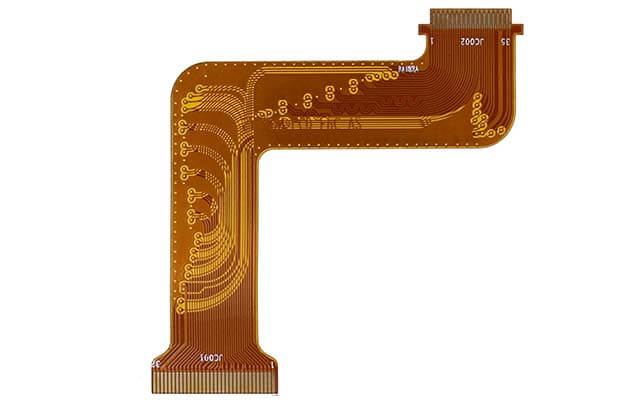
2 layer flexible PCB has two conductive copper layers and two coverlays. We can offer different colors of solder masks including green, black, white, yellow, blue, and red. It depends on our customers, typically we use coverlay to take place of the solder mask and the color of coverlay is yellow.
As an ISO-certified PCB company, we always provide high quality for you. There are different test methods to control the product quality including AOI inspection, flying probe test, and auto-fixture tester.
If you have one project that needs to be produced in a hurry, SMTFAB can help you to make it. We can produce the prototype of 2 layer flexible PCB within 24H and ship it by UPS, FedEx, or DHL.
You will send any type of 2 layer flexible PCB to us, please see its specifications as below:
The standard board thickness is 1/2mil to 3mil;
The copper thickness is 1/3oz to 2oz;
The surface finishes are Immersion gold, hard gold fingers.
2 Layer Flexible PCB
We have full service for quick-turn jobs and state-of-the-art equipment. It can meet your complicated project deadlines and budgets.
There are many different applications for 2 layer flexible PCB, such as aerospace, military & defense, automotive, medical devices, smartphones, GPS systems, motion systems, and Satellites.
Are you looking for a leading 2 layer flexible PCB supplier? SMTFAB is your best choice. SMTFAB has over 500 workers in our workshop and the monthly capacity is 40,000 square meters.
Do not hesitate to email us when you need our help.
2 Layer Flexible PCB: The Ultimate FAQ Guide
Are you interested in 2 layer flexible PCB?
In this guide, you will know more about 2 layer flexible PCBs. Let’s read it.
- What Are The Flexible PCBs?
- What Type Of Material Do The Manufacturers Use To Produce These 2 layer Flexible PCBs?
- What Is The Design And Manufacturing Process Of 2 Layer Flexible PCBs?
- Which Material Is Used 2 Layer Flexible PCB?
- What Is 2 layer Flexible PCB Stack-Up?
- How Is Manufacturing And Assembly Of 2 layer Flexible PCB Done?
- What Is the Cost Of 2 layer Flexible PCB Manufacturing Process?
- What Are Applications Of 2 Layer Flexible PCBs?
What Are The Flexible PCBs?
Flexible circuit boards, also called flexible PCBs or Flex PCBs, can easily conform to any product’s requirements.
Flexible PCBs contain specific circuit designs on their surface. For flexible PCBs, electronic parts are arranged on the base material called flexible laminate.
The flexible laminate allows the circuit to bend in various directions and enhances its freedom degree of electrical and mechanical design.
Flexible PCBs are especially useful in modular electronic structures.
Their applications include wireless floating heads, repeaters, digital cameras, cell phones, flat-panel LED displays, and HDI PCB.
Flexible PCB
What Type Of Material Do The Manufacturers Use To Produce These 2 layer Flexible PCBs?
A 2 layer flexible PCB is a circuit of two conductive membranes, one on either side of the circuit’s polyimide frame.
Trace designs, unique to your needs, can be produced on both sides of the substrate and linked via copper-plated through-holes.
The holes plated allow electrical contacts in both layers.
2 layer flexible PCBs assist in making Sculptured Flex boards.
They also allow higher circuit density when a layout cannot be routed on a single layer
What Is The Design And Manufacturing Process Of 2 Layer Flexible PCBs?
The 2 layer flexible PCB design can achieve optimum performance if a multitude of factors is taken into account.
Following are a few of the most important ones.
Layouts
Several simple forms of 2 layer flexible PCBs are available. There is a substantial difference in construction between various flexible PCB forms.
Single-side Flexible Layout
A single metal conductor sheet or a metal-filled conductive polymer on a thin dielectric film makes up single-sided flexible circuits. Component terminals may be reached from one side. Single-side flexible PCBs may or may not use protective coatings, including cover layers or cover coatings; however, the common practice is to use protective film over circuits.
2 layer flexible PCB Layout
2 layer flexible PCB circuits have two conducting layers. Their construction may or may not include plated through-holes.
However, the plated through hole variation is predominant.
Due to plated through-holes, connections for electronic components interfaces are provided for both sides of the circuit, enabling component placement on both sides of the flexible PCB.
If the design requires, protective cover layers may be applied on both sides of 2 layer flexible PCB.
However, the manufacturers do not miss applying a protective cover film or coating.
2 Layer Flexible PCB
Multilayer Flexible Layout
Flexible PCBs with three or more conductors’ layers are known as multilayer flex circuits.
Typically, the layers are linked via plated through-holes, but this is not compulsory.
Discontinuous lamination is standard in cases that require maximum flexibility.
And it is accomplished by leaving areas where frequent stretching, twisting, or bending is to happen.
Rigid-Flex Layout
Rigid-flex circuits are hybrid constructions consisting of rigid and flexible substrates laminated together into a single structure.
They are then sequentially electrically interconnected using plated through-holes.
Rigid-flex boards are often considered a specialty product for low-volume applications because of manufacturing challenges.
Therefore, flex technology has advanced into the commercial and business world in recent years.
Rigid-Flex PCB
Which Material Is Used 2 Layer Flexible PCB?
The most common 2 layer flexible PCBs material is copper, copper foil, and alloys such as gold, silver, nickel, and aluminum.
Two types of copper foils rolled and annealed (RA) and electrodeposited (ED), are prevalent.
The RA foil is smooth and uniformly structured, while the ED is sturdy, but it cannot withstand the etching or roughening process.
Moreover, the photosensitive polyimide coating is also commonly used. It allows for higher component density and excellent dimensional stability.
Typical base materials for 2 layer flexible PCBs include films, foils, and adhesives. Polyethylene naphthalate (PEN) and Liquid Crystal Polymer (LCP) are among the recently evolving materials.
LCP materials absorb less moisture, avoiding the baking process, usually carried out in polyimide manufacturing.
Ultimately, the choice of material relies on the way the circuit would be assembled and used.
Choosing the right materials for flexible PCBs is vital.
Available space, target performance, and product cost are all critical when selecting a PCB material.
Therefore, an optimal tradeoff between the price and the PCB performance results in the best outcomes.
Following are some features necessary for flexible PCB material selection.
FR4
FR4 is a material grade rather than a category term. It is a flame-resistant substance that, once ignited, self-extinguishes.
A variety of FR-4 grade materials are constructed of composite materials. The electrical insulation properties of FR4 are consistent.
They have a smooth surface and a plane. The thickness resistance of FR4 makes it perfect for high-performance insulation applications.
The dielectric constant of FR4 is approximately 4.5, and it can tolerate temperatures of up to 130 degrees Celsius.
There are also FR2 and FR3 laminates available. Postfixes two, three, and four show how much heat and a temperature it can handle.
Polyester
Polyester is a brand name for Polyethylene Terephthalate (PET). It is a commonly used commodity in flexible PCBs production.
PETs are noted for their high chemical and moisture tolerance, flexibility, and excellent electrical properties.
Lightweight PETS are suitable for producing compact 2 layer flexible PCBs. PET resin has outstanding mechanical properties.
However, it has a low heat tolerance, making direct soldering and assembly difficult.
Polyimide
Polyimide, in the form of polymeric film, serves as the flexible PCB substrate.
Mechanically, it is durable and heat resistant.
Polyimides are fire-proof and resistant to oils and solvents.
High-temperature tolerance and strong bending strength are two benefits of polyimide resin insulation.
Polyimide films are also effective in high-reliability applications, including military, medical, and dynamic flex.
Polyimides are used in sensors, calculators, and instrument interface panels. Polyimide also has temperature flexibility, better electrical properties, more robust chemical and tear tolerance, and higher tensile strength.
2 Layer Flexible PCB
Polyether Ether Ketone
PEEK (polyether ether ketone) is a chemically resistant material that can sustain higher radiation.
They have a strong melting point and a broader heat resistance spectrum to not melt at high temperatures.
PEEK-based materials are used in healthcare devices, such as X-ray machines. They are commonly used as a PCB cover layer and in aircraft electrical systems.
While the PEEKs are elastic and resilient, their tear strength needs improving.
Polytetrafluorethylene
PTFE such as RO3000 and RO4000 is as simple to produce as FR-4.
They have low dielectric losses at microwave frequencies, allowing them to operate at higher frequencies for longer.
PTFE also works well in multilayer PCB. It has tight thickness tolerances, ensuring outstanding accuracy in a variety of applications.
PTFE also makes for a good balance between low dissipation and high-temperature stability.
Antennas, car cruise control, power amplifiers, and aerospace guidance telemetry benefit from these components.
PTFE is used as a nonstick coating on frying pans in real life.
What Is 2 layer Flexible PCB Stack-Up?
2 layer flexible PCB comprises a central base film called a laminate or a substrate, two copper foils, up to four adhesive layers, and two covering or protective layers.
Base films contain plated-through holes that connect to copper foil layers.
Adhesive layers attach a copper layer to the base film and attach a protective coating to the copper foil layer on both flexible PCB sides.
2 layer flexible PCB stackup(1)
2 layer Flexible PCB stackup(2)
How Is Manufacturing And Assembly Of 2 layer Flexible PCB Done?
There are numerous flexible circuit constructions in use. There is a wide variety of materials and processes used in these constructions.
The correct choice of manufacturing method depends on the end product’s objectives and what can be traded off, if necessary, with the most negligible impact on the finished product.
A close working relationship is essential between the designer and the manufacturer to ensure the right balance between design intentions and manufacturing choices.
So, the flexible circuits offer some novel challenges to the assembly process.
How Is Single Conductor Layer Flex Manufactured?
Single-sided flex circuits are a combination of ease and low cost. It is the predominant form of circuit construction.
A large part of the industry’s success and growth is due to the manufacturing of single-sided flex.
An essential list of methods for creating flexible circuits includes additive, semi-additive, semi-subtractive, and subtractive processes.
What are Additive and Subtractive Processing?
Its use is infrequent in flex circuit processing but has massive potential.
Typically, a catalyzed laminate serves as a base for negative image placement of the circuit patterns.
The exposed laminate can then be plated up to shape up the required circuit patterns.
Subtractive, or print-and-etch, is a typically used approach for producing flex circuits.
Circuits are manufactured by printing the circuit image on a metal foil-clad dielectric’s metal surface using a suitable etch-resistant polymer.
What is Die-Cut Processing?
Die-cut processing has seen development in applications where coarse circuit features are a design necessity.
Examples of die-cut processing consist of power bus circuits and automobile clusters.
So, in high-volume applications, this approach has proven practical and economical.
What are Back Bared Flexible Circuits?
Back bared circuits contain a single conductor layer that is accessible from both sides.
The back-access technique is typically employed when component soldering or another interconnection method is required on two sides of the circuit.
There are many approaches for producing a back-bared, single-conductor layer circuit.
One is polyimide chemical etching. It is beneficial for fabrication using polyimide films. Polyimide dissolves in hot, strongly alkaline solutions. Additively and semi-additively processed flexible circuits were not prevalent a few years ago.
Additive fabrication produces large numbers of finer lines and spaces on flex circuit boards.
What are Imaging and Etching Processes?
Proper management of flexible materials during imaging and etching is crucial.
Special tools can address any concerns that arise due to manual human work.
Screen printing is the oldest process. It involves printing a chemically resistant ink in the circuit’s pattern directly onto a copper-clad laminate.
Photolithographic techniques (positive or negative) generate the circuit patterns. The water wets the panel’s surface before lamination during manufacturing.
A slight indentation in the copper foil can cause a short or open in the final circuit. In any case, precleaning of the flexible copper-clad laminate is essential.
The other type of imaging machine, referred to as a direct imaging machine, draws the circuit pattern directly onto the board.
There is almost no recovery from an over-etched condition. The copper must be clean and free of any development residue since such materials can delay or prevent etching.
The process of etching is the most commonly shared among all circuit types.
What Is the Cost Of 2 layer Flexible PCB Manufacturing Process?
2 layer Flexible PCBs cost more than single-sided or rigid PCBs.
The raw materials and dedicated parts for specific functional needs are the primary cost drivers. Some design approaches can limit costs if implemented correctly.
An experienced, flexible PCB manufacturer must flexible product and efficiently manage output costs.
Therefore, many designs can be optimized to save costs and reduce complexity by eliminating extra layers. Some important considerations for enhanced design are listed below.
- The most crucial aspect of design optimization is the number of layers. Hence, if a single layer can accomplish the purpose, then avoid extra layers.
- There are many flexible PCB types. Each type has its own cost and performance specification. The parameters that decide price usually include material utilization rate, number of layers, degree of flexibility, timeline, and circuit complexity.
- 2 to 3 mil track spacing and 0.25 mil hole size usually is optimal because it does the job in most cases, and it is not too expensive.
- There are two options for flex PCB gold fingers, hard gold or immersion gold. Hard gold is costly.
- PCB stiffener is an important parameter. There are three options for stiffeners, Pi stiffener, Fr4 stiffener, and Aluminum stiffener. So, for high-frequency applications, a harder stiffener is advisable.
- Low copper thickness is better. For higher flexibility circuits, avoid heavy copper. Instead, 1/3 oz copper is optimal.
- The standard immersion gold finish is generally profitable.
- A higher material utilization rate keeps the cost considerably down.
- Manufacturing in higher quantities is usually more cost-effective.
2 Layer Flexible PCB
What Are Applications Of 2 Layer Flexible PCBs?
The usage of flexible and 2 layer flexible PCB devices is becoming more popular.
The 2 layer flexible PCBs are being used in novel forms by designers.
In IC packaging, modern, flexible circuit technology has a significant part density.
These PCBs are widely used in digital cameras today.
The flexible sensors can detect vibrations, humidity, radiation, temperature, light, heat, and chemicals.
They can track livestock and control patients when implanted in RFID systems.
Calculators, printers, computers, cellphones, and other mobile devices utilize modular 2 layer flexible PCBs. Sensory equipment, robotics, and a human-machine interface are all examples of flexible PCB implementations.
The 2 layer flexible PCBs have applications in the automobile industry. Hearing aids, pacemakers, and exercise devices all utilize adjustable circuits, particularly convenient healthcare.
In recent years, progress on flexible thin-film solar cells has accelerated. They’re lightweight, allowing for mass manufacturing at a low cost. Rollup solar cell arrays allow for electricity storage for defensive purposes.
Other 2 layer flexible PCB Applications might include:
- Ground and power plane applications.
- Dense surface mount assembly.
- Protective and shielding applications.
- LCD Module for cellphones, laptops, digital cameras, and calculators.
- Optical pick-up for autonomous vehicles and computers.
Your Experienced 2 Layer Flexible PCB Manufacturer in China
SMTFAB is a Professional 2 layer flexible PCB supplier in China, and we can provide a one-stop solution for your project.
- Over 12 years 2 layer flexible PCB manufacturing experience
- All 2 layer flexible PCBs meet IPC Class 2 or 3
- 100% E-test and AOI inspection
- Offer a free sample before your mass production order
- 24h quick-turn service for your prototype 2 layer flexible PCB
- 7/24 sales and engineering tech support
- Production Facility
- Flexible PCB Capabilities
- 2layer Flex PCB Stackup
For flexible PCB capabilities, please refer to the following form.
| Feature | Capability | |||||||
| Number of Layers | 1 – 10layers | |||||||
| Order Quantity | 1pc – 10000+pcs | |||||||
| Board thickness(without stiffener) | 0.002-0.2inch | |||||||
| Min. Board Size | 0.2*0.4inch | |||||||
| Min. Board Size | 9*14 inch | |||||||
| Build Time | 2days – 5weeks | |||||||
| Material | FCCL (adhesive) | Shengyi SF305 | ||||||
| FCCL (adhesiveness) | Panasonic R-F775 | |||||||
| Taiflex MHK | ||||||||
| Dupont Pyralux AP | ||||||||
| Coverlay | Shengyi SF305C | |||||||
| Taiflex FHK 1025&2035 | ||||||||
| Adhesive | Taiflex BT | |||||||
| PI stiffener | Taiflex MHK | |||||||
| 3M | 9077&6677&9058 | |||||||
| Others | Tolerance of single layer | ±0.05mm | ||||||
| Tolerance of double-layer (≤0.3mm) | ±0.05mm | |||||||
| Tolerance of multi-layer(<0.3mm) | ±0.05mm | |||||||
| Tolerance of multi-layer(0.3-0.8mm) | ±0.1mm | |||||||
| Impedance control tolerance | Single ended:±5Ω(≤50Ω);±10%(>50Ω) | |||||||
| Differential Pairs: ±5Ω (≤50Ω);±10%(>50Ω) | ||||||||
| Min coverlay bridge | 8mil | |||||||
| Min bend radius of single layer | 3-6 times of board thickness | |||||||
| Min bend radius of double-layer | 6-10 times of board thickness | |||||||
| Min bend radius of multilayer | 10-15 times of board thickness | |||||||
| Min dynamic bend radius | 20-40 times of board thickness | |||||||
| Inner layer | Min line width/spacing (12/18um copper) | 3.0/3.2mil (loop lines 6.0/6.2mil) | ||||||
| Min line width/spacing (35um copper) | 4.0/4.0mil (loop lines 8.0/8.0mil) | |||||||
| Min line width/spacing (70um copper) | 6.0/6.5mil (loop lines 10/10.5mil) | |||||||
| Max copper thickness | 2oz | |||||||
| Outer layer | Min line width/spacing (18um copper) | 3/3.2mil (loop lines 6/6mil) | ||||||
| Min line width/spacing (35um copper) | 4/4.5mil (loop lines 6/6mil) | |||||||
| Min line width/spacing (70um copper) | 6/7mil (loop lines 6/6mil) | |||||||
| Min line width/spacing (105um copper) | 10/13mil (loop lines 6/6mil) | |||||||
| Max finished copper thickness | 3OZ | |||||||
| Drilling | Min distance between via and conductors | 6mil (<4 layer) | ||||||
| 8mil (4-6 layer) | ||||||||
| 12mil (7-8 layer) | ||||||||
| Min mechanical drill hole | 6mil | |||||||
| Solder mask | Solder mask color | Green/White/Black/Yellow | ||||||
| and silkscreen | Coverlay | Yellow、Black | ||||||
| Min solder dam (base copper ≤ 1OZ) | 4mil (green),8mil(solder dam on the large copper) | |||||||
| Min clearance | 3mil (part for 2.5mil) | |||||||
| Silk color | White, Yellow | |||||||
| Surface treatment | Surface treatment | HASL, ENIG, ENEPIG, Electrolytic Nickel Gold, Soft gold, Hard gold, | ||||||
| Immersion silver and OSP | ||||||||
| Mixed surface treatment | ENIG+OSP, ENIG+G/F | |||||||
| Gold thickness (ENIG) | 0.05-0.10um | |||||||
| Nickel thickness (ENIG) | 3-6um | |||||||
| Gold thickness (ENEPIG) | 0.05-0.10um | |||||||
| Palladium thickness (ENEPIG) | 0.05-0.15um | |||||||
| Nick thickness (ENEPIG) | 3-6um | |||||||
| Electrolytic nickel thickness | 3-6um | |||||||
| Electrolytic gold thickness | 0.05-0.10um | |||||||
| Hard gold thickness (including lead) | 0.1-1.5um | |||||||
| OSP thickness | 0.1-0.3um | |||||||
| Immersion silver thickness | 0.2-0.4um | |||||||
| Routing | Laser accuracy | ±0.05mm | ||||||
| Punch accuracy | ±0.05mm–±0.15mm | |||||||
Please see the details of 2 layer Flex PCB Stack-up as follows:
Releted Some Other PCBs
Why Choose SMTFAB for Your 2 Layer Flexible PCB
Double-sided flexible PCBs or double-layer flex PCBs or 2 layer flexible PCBs are very popular in the electronic industry.
As a reliable 2 layer PCB manufacturer in China, SMTFAB can provide PCB design & layout, PCB fabrication, and PCB assembly. If you are looking for a turnkey solution provider, SMTFAB is your best choice.
2 layer flexible PCB has two conductive copper layers and two coverlays. We can offer different colors of solder masks including green, black, white, yellow, blue, and red. It depends on our customers, typically we use coverlay to take place of the solder mask and the color of coverlay is yellow.
As an ISO-certified PCB company, we always provide high quality for you. There are different test methods to control the product quality including AOI inspection, flying probe test, and auto-fixture tester.
If you have one project that needs to be produced in a hurry, SMTFAB can help you to make it. We can produce the prototype of 2 layer flexible PCB within 24H and ship it by UPS, FedEx, or DHL.
You will send any type of 2 layer flexible PCB to us, please see its specifications as below:
The standard board thickness is 1/2mil to 3mil;
The copper thickness is 1/3oz to 2oz;
The surface finishes are Immersion gold, hard gold fingers.
2 Layer Flexible PCB
We have full service for quick-turn jobs and state-of-the-art equipment. It can meet your complicated project deadlines and budgets.
There are many different applications for 2 layer flexible PCB, such as aerospace, military & defense, automotive, medical devices, smartphones, GPS systems, motion systems, and Satellites.
Are you looking for a leading 2 layer flexible PCB supplier? SMTFAB is your best choice. SMTFAB has over 500 workers in our workshop and the monthly capacity is 40,000 square meters.
Do not hesitate to email us when you need our help.
2 Layer Flexible PCB: The Ultimate FAQ Guide
Are you interested in 2 layer flexible PCB?
In this guide, you will know more about 2 layer flexible PCBs. Let’s read it.
- What Are The Flexible PCBs?
- What Type Of Material Do The Manufacturers Use To Produce These 2 layer Flexible PCBs?
- What Is The Design And Manufacturing Process Of 2 Layer Flexible PCBs?
- Which Material Is Used 2 Layer Flexible PCB?
- What Is 2 layer Flexible PCB Stack-Up?
- How Is Manufacturing And Assembly Of 2 layer Flexible PCB Done?
- What Is the Cost Of 2 layer Flexible PCB Manufacturing Process?
- What Are Applications Of 2 Layer Flexible PCBs?
What Are The Flexible PCBs?
Flexible circuit boards, also called flexible PCBs or Flex PCBs, can easily conform to any product’s requirements.
Flexible PCBs contain specific circuit designs on their surface. For flexible PCBs, electronic parts are arranged on the base material called flexible laminate.
The flexible laminate allows the circuit to bend in various directions and enhances its freedom degree of electrical and mechanical design.
Flexible PCBs are especially useful in modular electronic structures.
Their applications include wireless floating heads, repeaters, digital cameras, cell phones, flat-panel LED displays, and HDI PCB.
Flexible PCB
What Type Of Material Do The Manufacturers Use To Produce These 2 layer Flexible PCBs?
A 2 layer flexible PCB is a circuit of two conductive membranes, one on either side of the circuit’s polyimide frame.
Trace designs, unique to your needs, can be produced on both sides of the substrate and linked via copper-plated through-holes.
The holes plated allow electrical contacts in both layers.
2 layer flexible PCBs assist in making Sculptured Flex boards.
They also allow higher circuit density when a layout cannot be routed on a single layer
What Is The Design And Manufacturing Process Of 2 Layer Flexible PCBs?
The 2 layer flexible PCB design can achieve optimum performance if a multitude of factors is taken into account.
Following are a few of the most important ones.
Layouts
Several simple forms of 2 layer flexible PCBs are available. There is a substantial difference in construction between various flexible PCB forms.
Single-side Flexible Layout
A single metal conductor sheet or a metal-filled conductive polymer on a thin dielectric film makes up single-sided flexible circuits. Component terminals may be reached from one side. Single-side flexible PCBs may or may not use protective coatings, including cover layers or cover coatings; however, the common practice is to use protective film over circuits.
2 layer flexible PCB Layout
2 layer flexible PCB circuits have two conducting layers. Their construction may or may not include plated through-holes.
However, the plated through hole variation is predominant.
Due to plated through-holes, connections for electronic components interfaces are provided for both sides of the circuit, enabling component placement on both sides of the flexible PCB.
If the design requires, protective cover layers may be applied on both sides of 2 layer flexible PCB.
However, the manufacturers do not miss applying a protective cover film or coating.
2 Layer Flexible PCB
Multilayer Flexible Layout
Flexible PCBs with three or more conductors’ layers are known as multilayer flex circuits.
Typically, the layers are linked via plated through-holes, but this is not compulsory.
Discontinuous lamination is standard in cases that require maximum flexibility.
And it is accomplished by leaving areas where frequent stretching, twisting, or bending is to happen.
Rigid-Flex Layout
Rigid-flex circuits are hybrid constructions consisting of rigid and flexible substrates laminated together into a single structure.
They are then sequentially electrically interconnected using plated through-holes.
Rigid-flex boards are often considered a specialty product for low-volume applications because of manufacturing challenges.
Therefore, flex technology has advanced into the commercial and business world in recent years.
Rigid-Flex PCB
Which Material Is Used 2 Layer Flexible PCB?
The most common 2 layer flexible PCBs material is copper, copper foil, and alloys such as gold, silver, nickel, and aluminum.
Two types of copper foils rolled and annealed (RA) and electrodeposited (ED), are prevalent.
The RA foil is smooth and uniformly structured, while the ED is sturdy, but it cannot withstand the etching or roughening process.
Moreover, the photosensitive polyimide coating is also commonly used. It allows for higher component density and excellent dimensional stability.
Typical base materials for 2 layer flexible PCBs include films, foils, and adhesives. Polyethylene naphthalate (PEN) and Liquid Crystal Polymer (LCP) are among the recently evolving materials.
LCP materials absorb less moisture, avoiding the baking process, usually carried out in polyimide manufacturing.
Ultimately, the choice of material relies on the way the circuit would be assembled and used.
Choosing the right materials for flexible PCBs is vital.
Available space, target performance, and product cost are all critical when selecting a PCB material.
Therefore, an optimal tradeoff between the price and the PCB performance results in the best outcomes.
Following are some features necessary for flexible PCB material selection.
FR4
FR4 is a material grade rather than a category term. It is a flame-resistant substance that, once ignited, self-extinguishes.
A variety of FR-4 grade materials are constructed of composite materials. The electrical insulation properties of FR4 are consistent.
They have a smooth surface and a plane. The thickness resistance of FR4 makes it perfect for high-performance insulation applications.
The dielectric constant of FR4 is approximately 4.5, and it can tolerate temperatures of up to 130 degrees Celsius.
There are also FR2 and FR3 laminates available. Postfixes two, three, and four show how much heat and a temperature it can handle.
Polyester
Polyester is a brand name for Polyethylene Terephthalate (PET). It is a commonly used commodity in flexible PCBs production.
PETs are noted for their high chemical and moisture tolerance, flexibility, and excellent electrical properties.
Lightweight PETS are suitable for producing compact 2 layer flexible PCBs. PET resin has outstanding mechanical properties.
However, it has a low heat tolerance, making direct soldering and assembly difficult.
Polyimide
Polyimide, in the form of polymeric film, serves as the flexible PCB substrate.
Mechanically, it is durable and heat resistant.
Polyimides are fire-proof and resistant to oils and solvents.
High-temperature tolerance and strong bending strength are two benefits of polyimide resin insulation.
Polyimide films are also effective in high-reliability applications, including military, medical, and dynamic flex.
Polyimides are used in sensors, calculators, and instrument interface panels. Polyimide also has temperature flexibility, better electrical properties, more robust chemical and tear tolerance, and higher tensile strength.
2 Layer Flexible PCB
Polyether Ether Ketone
PEEK (polyether ether ketone) is a chemically resistant material that can sustain higher radiation.
They have a strong melting point and a broader heat resistance spectrum to not melt at high temperatures.
PEEK-based materials are used in healthcare devices, such as X-ray machines. They are commonly used as a PCB cover layer and in aircraft electrical systems.
While the PEEKs are elastic and resilient, their tear strength needs improving.
Polytetrafluorethylene
PTFE such as RO3000 and RO4000 is as simple to produce as FR-4.
They have low dielectric losses at microwave frequencies, allowing them to operate at higher frequencies for longer.
PTFE also works well in multilayer PCB. It has tight thickness tolerances, ensuring outstanding accuracy in a variety of applications.
PTFE also makes for a good balance between low dissipation and high-temperature stability.
Antennas, car cruise control, power amplifiers, and aerospace guidance telemetry benefit from these components.
PTFE is used as a nonstick coating on frying pans in real life.
What Is 2 layer Flexible PCB Stack-Up?
2 layer flexible PCB comprises a central base film called a laminate or a substrate, two copper foils, up to four adhesive layers, and two covering or protective layers.
Base films contain plated-through holes that connect to copper foil layers.
Adhesive layers attach a copper layer to the base film and attach a protective coating to the copper foil layer on both flexible PCB sides.
2 layer flexible PCB stackup(1)
2 layer Flexible PCB stackup(2)
How Is Manufacturing And Assembly Of 2 layer Flexible PCB Done?
There are numerous flexible circuit constructions in use. There is a wide variety of materials and processes used in these constructions.
The correct choice of manufacturing method depends on the end product’s objectives and what can be traded off, if necessary, with the most negligible impact on the finished product.
A close working relationship is essential between the designer and the manufacturer to ensure the right balance between design intentions and manufacturing choices.
So, the flexible circuits offer some novel challenges to the assembly process.
How Is Single Conductor Layer Flex Manufactured?
Single-sided flex circuits are a combination of ease and low cost. It is the predominant form of circuit construction.
A large part of the industry’s success and growth is due to the manufacturing of single-sided flex.
An essential list of methods for creating flexible circuits includes additive, semi-additive, semi-subtractive, and subtractive processes.
What are Additive and Subtractive Processing?
Its use is infrequent in flex circuit processing but has massive potential.
Typically, a catalyzed laminate serves as a base for negative image placement of the circuit patterns.
The exposed laminate can then be plated up to shape up the required circuit patterns.
Subtractive, or print-and-etch, is a typically used approach for producing flex circuits.
Circuits are manufactured by printing the circuit image on a metal foil-clad dielectric’s metal surface using a suitable etch-resistant polymer.
What is Die-Cut Processing?
Die-cut processing has seen development in applications where coarse circuit features are a design necessity.
Examples of die-cut processing consist of power bus circuits and automobile clusters.
So, in high-volume applications, this approach has proven practical and economical.
What are Back Bared Flexible Circuits?
Back bared circuits contain a single conductor layer that is accessible from both sides.
The back-access technique is typically employed when component soldering or another interconnection method is required on two sides of the circuit.
There are many approaches for producing a back-bared, single-conductor layer circuit.
One is polyimide chemical etching. It is beneficial for fabrication using polyimide films. Polyimide dissolves in hot, strongly alkaline solutions. Additively and semi-additively processed flexible circuits were not prevalent a few years ago.
Additive fabrication produces large numbers of finer lines and spaces on flex circuit boards.
What are Imaging and Etching Processes?
Proper management of flexible materials during imaging and etching is crucial.
Special tools can address any concerns that arise due to manual human work.
Screen printing is the oldest process. It involves printing a chemically resistant ink in the circuit’s pattern directly onto a copper-clad laminate.
Photolithographic techniques (positive or negative) generate the circuit patterns. The water wets the panel’s surface before lamination during manufacturing.
A slight indentation in the copper foil can cause a short or open in the final circuit. In any case, precleaning of the flexible copper-clad laminate is essential.
The other type of imaging machine, referred to as a direct imaging machine, draws the circuit pattern directly onto the board.
There is almost no recovery from an over-etched condition. The copper must be clean and free of any development residue since such materials can delay or prevent etching.
The process of etching is the most commonly shared among all circuit types.
What Is the Cost Of 2 layer Flexible PCB Manufacturing Process?
2 layer Flexible PCBs cost more than single-sided or rigid PCBs.
The raw materials and dedicated parts for specific functional needs are the primary cost drivers. Some design approaches can limit costs if implemented correctly.
An experienced, flexible PCB manufacturer must flexible product and efficiently manage output costs.
Therefore, many designs can be optimized to save costs and reduce complexity by eliminating extra layers. Some important considerations for enhanced design are listed below.
- The most crucial aspect of design optimization is the number of layers. Hence, if a single layer can accomplish the purpose, then avoid extra layers.
- There are many flexible PCB types. Each type has its own cost and performance specification. The parameters that decide price usually include material utilization rate, number of layers, degree of flexibility, timeline, and circuit complexity.
- 2 to 3 mil track spacing and 0.25 mil hole size usually is optimal because it does the job in most cases, and it is not too expensive.
- There are two options for flex PCB gold fingers, hard gold or immersion gold. Hard gold is costly.
- PCB stiffener is an important parameter. There are three options for stiffeners, Pi stiffener, Fr4 stiffener, and Aluminum stiffener. So, for high-frequency applications, a harder stiffener is advisable.
- Low copper thickness is better. For higher flexibility circuits, avoid heavy copper. Instead, 1/3 oz copper is optimal.
- The standard immersion gold finish is generally profitable.
- A higher material utilization rate keeps the cost considerably down.
- Manufacturing in higher quantities is usually more cost-effective.
2 Layer Flexible PCB
What Are Applications Of 2 Layer Flexible PCBs?
The usage of flexible and 2 layer flexible PCB devices is becoming more popular.
The 2 layer flexible PCBs are being used in novel forms by designers.
In IC packaging, modern, flexible circuit technology has a significant part density.
These PCBs are widely used in digital cameras today.
The flexible sensors can detect vibrations, humidity, radiation, temperature, light, heat, and chemicals.
They can track livestock and control patients when implanted in RFID systems.
Calculators, printers, computers, cellphones, and other mobile devices utilize modular 2 layer flexible PCBs. Sensory equipment, robotics, and a human-machine interface are all examples of flexible PCB implementations.
The 2 layer flexible PCBs have applications in the automobile industry. Hearing aids, pacemakers, and exercise devices all utilize adjustable circuits, particularly convenient healthcare.
In recent years, progress on flexible thin-film solar cells has accelerated. They’re lightweight, allowing for mass manufacturing at a low cost. Rollup solar cell arrays allow for electricity storage for defensive purposes.
Other 2 layer flexible PCB Applications might include:
- Ground and power plane applications.
- Dense surface mount assembly.
- Protective and shielding applications.
- LCD Module for cellphones, laptops, digital cameras, and calculators.
- Optical pick-up for autonomous vehicles and computers.
Your Experienced 2 Layer Flexible PCB Manufacturer in China
SMTFAB is a Professional 2 layer flexible PCB supplier in China, and we can provide a one-stop solution for your project.
- Over 12 years 2 layer flexible PCB manufacturing experience
- All 2 layer flexible PCBs meet IPC Class 2 or 3
- 100% E-test and AOI inspection
- Offer a free sample before your mass production order
- 24h quick-turn service for your prototype 2 layer flexible PCB
- 7/24 sales and engineering tech support
Your Experienced 2 Layer Flexible PCB Manufacturer in China
Your Experienced 2 Layer Flexible PCB Manufacturer in China
SMTFAB is a Professional 2 layer flexible PCB supplier in China, and we can provide a one-stop solution for your project.
- Over 12 years 2 layer flexible PCB manufacturing experience
- All 2 layer flexible PCBs meet IPC Class 2 or 3
- 100% E-test and AOI inspection
- Offer a free sample before your mass production order
- 24h quick-turn service for your prototype 2 layer flexible PCB
- 7/24 sales and engineering tech support
- Production Facility
- Flexible PCB Capabilities
- 2layer Flex PCB Stackup
For flexible PCB capabilities, please refer to the following form.
| Feature | Capability | |||||||
| Number of Layers | 1 – 10layers | |||||||
| Order Quantity | 1pc – 10000+pcs | |||||||
| Board thickness(without stiffener) | 0.002-0.2inch | |||||||
| Min. Board Size | 0.2*0.4inch | |||||||
| Min. Board Size | 9*14 inch | |||||||
| Build Time | 2days – 5weeks | |||||||
| Material | FCCL (adhesive) | Shengyi SF305 | ||||||
| FCCL (adhesiveness) | Panasonic R-F775 | |||||||
| Taiflex MHK | ||||||||
| Dupont Pyralux AP | ||||||||
| Coverlay | Shengyi SF305C | |||||||
| Taiflex FHK 1025&2035 | ||||||||
| Adhesive | Taiflex BT | |||||||
| PI stiffener | Taiflex MHK | |||||||
| 3M | 9077&6677&9058 | |||||||
| Others | Tolerance of single layer | ±0.05mm | ||||||
| Tolerance of double-layer (≤0.3mm) | ±0.05mm | |||||||
| Tolerance of multi-layer(<0.3mm) | ±0.05mm | |||||||
| Tolerance of multi-layer(0.3-0.8mm) | ±0.1mm | |||||||
| Impedance control tolerance | Single ended:±5Ω(≤50Ω);±10%(>50Ω) | |||||||
| Differential Pairs: ±5Ω (≤50Ω);±10%(>50Ω) | ||||||||
| Min coverlay bridge | 8mil | |||||||
| Min bend radius of single layer | 3-6 times of board thickness | |||||||
| Min bend radius of double-layer | 6-10 times of board thickness | |||||||
| Min bend radius of multilayer | 10-15 times of board thickness | |||||||
| Min dynamic bend radius | 20-40 times of board thickness | |||||||
| Inner layer | Min line width/spacing (12/18um copper) | 3.0/3.2mil (loop lines 6.0/6.2mil) | ||||||
| Min line width/spacing (35um copper) | 4.0/4.0mil (loop lines 8.0/8.0mil) | |||||||
| Min line width/spacing (70um copper) | 6.0/6.5mil (loop lines 10/10.5mil) | |||||||
| Max copper thickness | 2oz | |||||||
| Outer layer | Min line width/spacing (18um copper) | 3/3.2mil (loop lines 6/6mil) | ||||||
| Min line width/spacing (35um copper) | 4/4.5mil (loop lines 6/6mil) | |||||||
| Min line width/spacing (70um copper) | 6/7mil (loop lines 6/6mil) | |||||||
| Min line width/spacing (105um copper) | 10/13mil (loop lines 6/6mil) | |||||||
| Max finished copper thickness | 3OZ | |||||||
| Drilling | Min distance between via and conductors | 6mil (<4 layer) | ||||||
| 8mil (4-6 layer) | ||||||||
| 12mil (7-8 layer) | ||||||||
| Min mechanical drill hole | 6mil | |||||||
| Solder mask | Solder mask color | Green/White/Black/Yellow | ||||||
| and silkscreen | Coverlay | Yellow、Black | ||||||
| Min solder dam (base copper ≤ 1OZ) | 4mil (green),8mil(solder dam on the large copper) | |||||||
| Min clearance | 3mil (part for 2.5mil) | |||||||
| Silk color | White, Yellow | |||||||
| Surface treatment | Surface treatment | HASL, ENIG, ENEPIG, Electrolytic Nickel Gold, Soft gold, Hard gold, | ||||||
| Immersion silver and OSP | ||||||||
| Mixed surface treatment | ENIG+OSP, ENIG+G/F | |||||||
| Gold thickness (ENIG) | 0.05-0.10um | |||||||
| Nickel thickness (ENIG) | 3-6um | |||||||
| Gold thickness (ENEPIG) | 0.05-0.10um | |||||||
| Palladium thickness (ENEPIG) | 0.05-0.15um | |||||||
| Nick thickness (ENEPIG) | 3-6um | |||||||
| Electrolytic nickel thickness | 3-6um | |||||||
| Electrolytic gold thickness | 0.05-0.10um | |||||||
| Hard gold thickness (including lead) | 0.1-1.5um | |||||||
| OSP thickness | 0.1-0.3um | |||||||
| Immersion silver thickness | 0.2-0.4um | |||||||
| Routing | Laser accuracy | ±0.05mm | ||||||
| Punch accuracy | ±0.05mm–±0.15mm | |||||||
Please see the details of 2 layer Flex PCB Stack-up as follows:
- Production Facility
- Flexible PCB Capabilities
- 2layer Flex PCB Stackup
For flexible PCB capabilities, please refer to the following form.
| Feature | Capability | |||||||
| Number of Layers | 1 – 10layers | |||||||
| Order Quantity | 1pc – 10000+pcs | |||||||
| Board thickness(without stiffener) | 0.002-0.2inch | |||||||
| Min. Board Size | 0.2*0.4inch | |||||||
| Min. Board Size | 9*14 inch | |||||||
| Build Time | 2days – 5weeks | |||||||
| Material | FCCL (adhesive) | Shengyi SF305 | ||||||
| FCCL (adhesiveness) | Panasonic R-F775 | |||||||
| Taiflex MHK | ||||||||
| Dupont Pyralux AP | ||||||||
| Coverlay | Shengyi SF305C | |||||||
| Taiflex FHK 1025&2035 | ||||||||
| Adhesive | Taiflex BT | |||||||
| PI stiffener | Taiflex MHK | |||||||
| 3M | 9077&6677&9058 | |||||||
| Others | Tolerance of single layer | ±0.05mm | ||||||
| Tolerance of double-layer (≤0.3mm) | ±0.05mm | |||||||
| Tolerance of multi-layer(<0.3mm) | ±0.05mm | |||||||
| Tolerance of multi-layer(0.3-0.8mm) | ±0.1mm | |||||||
| Impedance control tolerance | Single ended:±5Ω(≤50Ω);±10%(>50Ω) | |||||||
| Differential Pairs: ±5Ω (≤50Ω);±10%(>50Ω) | ||||||||
| Min coverlay bridge | 8mil | |||||||
| Min bend radius of single layer | 3-6 times of board thickness | |||||||
| Min bend radius of double-layer | 6-10 times of board thickness | |||||||
| Min bend radius of multilayer | 10-15 times of board thickness | |||||||
| Min dynamic bend radius | 20-40 times of board thickness | |||||||
| Inner layer | Min line width/spacing (12/18um copper) | 3.0/3.2mil (loop lines 6.0/6.2mil) | ||||||
| Min line width/spacing (35um copper) | 4.0/4.0mil (loop lines 8.0/8.0mil) | |||||||
| Min line width/spacing (70um copper) | 6.0/6.5mil (loop lines 10/10.5mil) | |||||||
| Max copper thickness | 2oz | |||||||
| Outer layer | Min line width/spacing (18um copper) | 3/3.2mil (loop lines 6/6mil) | ||||||
| Min line width/spacing (35um copper) | 4/4.5mil (loop lines 6/6mil) | |||||||
| Min line width/spacing (70um copper) | 6/7mil (loop lines 6/6mil) | |||||||
| Min line width/spacing (105um copper) | 10/13mil (loop lines 6/6mil) | |||||||
| Max finished copper thickness | 3OZ | |||||||
| Drilling | Min distance between via and conductors | 6mil (<4 layer) | ||||||
| 8mil (4-6 layer) | ||||||||
| 12mil (7-8 layer) | ||||||||
| Min mechanical drill hole | 6mil | |||||||
| Solder mask | Solder mask color | Green/White/Black/Yellow | ||||||
| and silkscreen | Coverlay | Yellow、Black | ||||||
| Min solder dam (base copper ≤ 1OZ) | 4mil (green),8mil(solder dam on the large copper) | |||||||
| Min clearance | 3mil (part for 2.5mil) | |||||||
| Silk color | White, Yellow | |||||||
| Surface treatment | Surface treatment | HASL, ENIG, ENEPIG, Electrolytic Nickel Gold, Soft gold, Hard gold, | ||||||
| Immersion silver and OSP | ||||||||
| Mixed surface treatment | ENIG+OSP, ENIG+G/F | |||||||
| Gold thickness (ENIG) | 0.05-0.10um | |||||||
| Nickel thickness (ENIG) | 3-6um | |||||||
| Gold thickness (ENEPIG) | 0.05-0.10um | |||||||
| Palladium thickness (ENEPIG) | 0.05-0.15um | |||||||
| Nick thickness (ENEPIG) | 3-6um | |||||||
| Electrolytic nickel thickness | 3-6um | |||||||
| Electrolytic gold thickness | 0.05-0.10um | |||||||
| Hard gold thickness (including lead) | 0.1-1.5um | |||||||
| OSP thickness | 0.1-0.3um | |||||||
| Immersion silver thickness | 0.2-0.4um | |||||||
| Routing | Laser accuracy | ±0.05mm | ||||||
| Punch accuracy | ±0.05mm–±0.15mm | |||||||
Please see the details of 2 layer Flex PCB Stack-up as follows:
Please see the details of 2 layer Flex PCB Stack-up as follows:
Releted Some Other PCBs
Releted Some Other PCBs
Why Choose SMTFAB for Your 2 Layer Flexible PCB
Double-sided flexible PCBs or double-layer flex PCBs or 2 layer flexible PCBs are very popular in the electronic industry.
As a reliable 2 layer PCB manufacturer in China, SMTFAB can provide PCB design & layout, PCB fabrication, and PCB assembly. If you are looking for a turnkey solution provider, SMTFAB is your best choice.
2 layer flexible PCB has two conductive copper layers and two coverlays. We can offer different colors of solder masks including green, black, white, yellow, blue, and red. It depends on our customers, typically we use coverlay to take place of the solder mask and the color of coverlay is yellow.
As an ISO-certified PCB company, we always provide high quality for you. There are different test methods to control the product quality including AOI inspection, flying probe test, and auto-fixture tester.
If you have one project that needs to be produced in a hurry, SMTFAB can help you to make it. We can produce the prototype of 2 layer flexible PCB within 24H and ship it by UPS, FedEx, or DHL.
You will send any type of 2 layer flexible PCB to us, please see its specifications as below:
The standard board thickness is 1/2mil to 3mil;
The copper thickness is 1/3oz to 2oz;
The surface finishes are Immersion gold, hard gold fingers.
2 Layer Flexible PCB
We have full service for quick-turn jobs and state-of-the-art equipment. It can meet your complicated project deadlines and budgets.
There are many different applications for 2 layer flexible PCB, such as aerospace, military & defense, automotive, medical devices, smartphones, GPS systems, motion systems, and Satellites.
Are you looking for a leading 2 layer flexible PCB supplier? SMTFAB is your best choice. SMTFAB has over 500 workers in our workshop and the monthly capacity is 40,000 square meters.
Do not hesitate to email us when you need our help.
2 Layer Flexible PCB: The Ultimate FAQ Guide
Are you interested in 2 layer flexible PCB?
In this guide, you will know more about 2 layer flexible PCBs. Let’s read it.
- What Are The Flexible PCBs?
- What Type Of Material Do The Manufacturers Use To Produce These 2 layer Flexible PCBs?
- What Is The Design And Manufacturing Process Of 2 Layer Flexible PCBs?
- Which Material Is Used 2 Layer Flexible PCB?
- What Is 2 layer Flexible PCB Stack-Up?
- How Is Manufacturing And Assembly Of 2 layer Flexible PCB Done?
- What Is the Cost Of 2 layer Flexible PCB Manufacturing Process?
- What Are Applications Of 2 Layer Flexible PCBs?
What Are The Flexible PCBs?
Flexible circuit boards, also called flexible PCBs or Flex PCBs, can easily conform to any product’s requirements.
Flexible PCBs contain specific circuit designs on their surface. For flexible PCBs, electronic parts are arranged on the base material called flexible laminate.
The flexible laminate allows the circuit to bend in various directions and enhances its freedom degree of electrical and mechanical design.
Flexible PCBs are especially useful in modular electronic structures.
Their applications include wireless floating heads, repeaters, digital cameras, cell phones, flat-panel LED displays, and HDI PCB.
Flexible PCB
What Type Of Material Do The Manufacturers Use To Produce These 2 layer Flexible PCBs?
A 2 layer flexible PCB is a circuit of two conductive membranes, one on either side of the circuit’s polyimide frame.
Trace designs, unique to your needs, can be produced on both sides of the substrate and linked via copper-plated through-holes.
The holes plated allow electrical contacts in both layers.
2 layer flexible PCBs assist in making Sculptured Flex boards.
They also allow higher circuit density when a layout cannot be routed on a single layer
What Is The Design And Manufacturing Process Of 2 Layer Flexible PCBs?
The 2 layer flexible PCB design can achieve optimum performance if a multitude of factors is taken into account.
Following are a few of the most important ones.
Layouts
Several simple forms of 2 layer flexible PCBs are available. There is a substantial difference in construction between various flexible PCB forms.
Single-side Flexible Layout
A single metal conductor sheet or a metal-filled conductive polymer on a thin dielectric film makes up single-sided flexible circuits. Component terminals may be reached from one side. Single-side flexible PCBs may or may not use protective coatings, including cover layers or cover coatings; however, the common practice is to use protective film over circuits.
2 layer flexible PCB Layout
2 layer flexible PCB circuits have two conducting layers. Their construction may or may not include plated through-holes.
However, the plated through hole variation is predominant.
Due to plated through-holes, connections for electronic components interfaces are provided for both sides of the circuit, enabling component placement on both sides of the flexible PCB.
If the design requires, protective cover layers may be applied on both sides of 2 layer flexible PCB.
However, the manufacturers do not miss applying a protective cover film or coating.
2 Layer Flexible PCB
Multilayer Flexible Layout
Flexible PCBs with three or more conductors’ layers are known as multilayer flex circuits.
Typically, the layers are linked via plated through-holes, but this is not compulsory.
Discontinuous lamination is standard in cases that require maximum flexibility.
And it is accomplished by leaving areas where frequent stretching, twisting, or bending is to happen.
Rigid-Flex Layout
Rigid-flex circuits are hybrid constructions consisting of rigid and flexible substrates laminated together into a single structure.
They are then sequentially electrically interconnected using plated through-holes.
Rigid-flex boards are often considered a specialty product for low-volume applications because of manufacturing challenges.
Therefore, flex technology has advanced into the commercial and business world in recent years.
Rigid-Flex PCB
Which Material Is Used 2 Layer Flexible PCB?
The most common 2 layer flexible PCBs material is copper, copper foil, and alloys such as gold, silver, nickel, and aluminum.
Two types of copper foils rolled and annealed (RA) and electrodeposited (ED), are prevalent.
The RA foil is smooth and uniformly structured, while the ED is sturdy, but it cannot withstand the etching or roughening process.
Moreover, the photosensitive polyimide coating is also commonly used. It allows for higher component density and excellent dimensional stability.
Typical base materials for 2 layer flexible PCBs include films, foils, and adhesives. Polyethylene naphthalate (PEN) and Liquid Crystal Polymer (LCP) are among the recently evolving materials.
LCP materials absorb less moisture, avoiding the baking process, usually carried out in polyimide manufacturing.
Ultimately, the choice of material relies on the way the circuit would be assembled and used.
Choosing the right materials for flexible PCBs is vital.
Available space, target performance, and product cost are all critical when selecting a PCB material.
Therefore, an optimal tradeoff between the price and the PCB performance results in the best outcomes.
Following are some features necessary for flexible PCB material selection.
FR4
FR4 is a material grade rather than a category term. It is a flame-resistant substance that, once ignited, self-extinguishes.
A variety of FR-4 grade materials are constructed of composite materials. The electrical insulation properties of FR4 are consistent.
They have a smooth surface and a plane. The thickness resistance of FR4 makes it perfect for high-performance insulation applications.
The dielectric constant of FR4 is approximately 4.5, and it can tolerate temperatures of up to 130 degrees Celsius.
There are also FR2 and FR3 laminates available. Postfixes two, three, and four show how much heat and a temperature it can handle.
Polyester
Polyester is a brand name for Polyethylene Terephthalate (PET). It is a commonly used commodity in flexible PCBs production.
PETs are noted for their high chemical and moisture tolerance, flexibility, and excellent electrical properties.
Lightweight PETS are suitable for producing compact 2 layer flexible PCBs. PET resin has outstanding mechanical properties.
However, it has a low heat tolerance, making direct soldering and assembly difficult.
Polyimide
Polyimide, in the form of polymeric film, serves as the flexible PCB substrate.
Mechanically, it is durable and heat resistant.
Polyimides are fire-proof and resistant to oils and solvents.
High-temperature tolerance and strong bending strength are two benefits of polyimide resin insulation.
Polyimide films are also effective in high-reliability applications, including military, medical, and dynamic flex.
Polyimides are used in sensors, calculators, and instrument interface panels. Polyimide also has temperature flexibility, better electrical properties, more robust chemical and tear tolerance, and higher tensile strength.
2 Layer Flexible PCB
Polyether Ether Ketone
PEEK (polyether ether ketone) is a chemically resistant material that can sustain higher radiation.
They have a strong melting point and a broader heat resistance spectrum to not melt at high temperatures.
PEEK-based materials are used in healthcare devices, such as X-ray machines. They are commonly used as a PCB cover layer and in aircraft electrical systems.
While the PEEKs are elastic and resilient, their tear strength needs improving.
Polytetrafluorethylene
PTFE such as RO3000 and RO4000 is as simple to produce as FR-4.
They have low dielectric losses at microwave frequencies, allowing them to operate at higher frequencies for longer.
PTFE also works well in multilayer PCB. It has tight thickness tolerances, ensuring outstanding accuracy in a variety of applications.
PTFE also makes for a good balance between low dissipation and high-temperature stability.
Antennas, car cruise control, power amplifiers, and aerospace guidance telemetry benefit from these components.
PTFE is used as a nonstick coating on frying pans in real life.
What Is 2 layer Flexible PCB Stack-Up?
2 layer flexible PCB comprises a central base film called a laminate or a substrate, two copper foils, up to four adhesive layers, and two covering or protective layers.
Base films contain plated-through holes that connect to copper foil layers.
Adhesive layers attach a copper layer to the base film and attach a protective coating to the copper foil layer on both flexible PCB sides.
2 layer flexible PCB stackup(1)
2 layer Flexible PCB stackup(2)
How Is Manufacturing And Assembly Of 2 layer Flexible PCB Done?
There are numerous flexible circuit constructions in use. There is a wide variety of materials and processes used in these constructions.
The correct choice of manufacturing method depends on the end product’s objectives and what can be traded off, if necessary, with the most negligible impact on the finished product.
A close working relationship is essential between the designer and the manufacturer to ensure the right balance between design intentions and manufacturing choices.
So, the flexible circuits offer some novel challenges to the assembly process.
How Is Single Conductor Layer Flex Manufactured?
Single-sided flex circuits are a combination of ease and low cost. It is the predominant form of circuit construction.
A large part of the industry’s success and growth is due to the manufacturing of single-sided flex.
An essential list of methods for creating flexible circuits includes additive, semi-additive, semi-subtractive, and subtractive processes.
What are Additive and Subtractive Processing?
Its use is infrequent in flex circuit processing but has massive potential.
Typically, a catalyzed laminate serves as a base for negative image placement of the circuit patterns.
The exposed laminate can then be plated up to shape up the required circuit patterns.
Subtractive, or print-and-etch, is a typically used approach for producing flex circuits.
Circuits are manufactured by printing the circuit image on a metal foil-clad dielectric’s metal surface using a suitable etch-resistant polymer.
What is Die-Cut Processing?
Die-cut processing has seen development in applications where coarse circuit features are a design necessity.
Examples of die-cut processing consist of power bus circuits and automobile clusters.
So, in high-volume applications, this approach has proven practical and economical.
What are Back Bared Flexible Circuits?
Back bared circuits contain a single conductor layer that is accessible from both sides.
The back-access technique is typically employed when component soldering or another interconnection method is required on two sides of the circuit.
There are many approaches for producing a back-bared, single-conductor layer circuit.
One is polyimide chemical etching. It is beneficial for fabrication using polyimide films. Polyimide dissolves in hot, strongly alkaline solutions. Additively and semi-additively processed flexible circuits were not prevalent a few years ago.
Additive fabrication produces large numbers of finer lines and spaces on flex circuit boards.
What are Imaging and Etching Processes?
Proper management of flexible materials during imaging and etching is crucial.
Special tools can address any concerns that arise due to manual human work.
Screen printing is the oldest process. It involves printing a chemically resistant ink in the circuit’s pattern directly onto a copper-clad laminate.
Photolithographic techniques (positive or negative) generate the circuit patterns. The water wets the panel’s surface before lamination during manufacturing.
A slight indentation in the copper foil can cause a short or open in the final circuit. In any case, precleaning of the flexible copper-clad laminate is essential.
The other type of imaging machine, referred to as a direct imaging machine, draws the circuit pattern directly onto the board.
There is almost no recovery from an over-etched condition. The copper must be clean and free of any development residue since such materials can delay or prevent etching.
The process of etching is the most commonly shared among all circuit types.
What Is the Cost Of 2 layer Flexible PCB Manufacturing Process?
2 layer Flexible PCBs cost more than single-sided or rigid PCBs.
The raw materials and dedicated parts for specific functional needs are the primary cost drivers. Some design approaches can limit costs if implemented correctly.
An experienced, flexible PCB manufacturer must flexible product and efficiently manage output costs.
Therefore, many designs can be optimized to save costs and reduce complexity by eliminating extra layers. Some important considerations for enhanced design are listed below.
- The most crucial aspect of design optimization is the number of layers. Hence, if a single layer can accomplish the purpose, then avoid extra layers.
- There are many flexible PCB types. Each type has its own cost and performance specification. The parameters that decide price usually include material utilization rate, number of layers, degree of flexibility, timeline, and circuit complexity.
- 2 to 3 mil track spacing and 0.25 mil hole size usually is optimal because it does the job in most cases, and it is not too expensive.
- There are two options for flex PCB gold fingers, hard gold or immersion gold. Hard gold is costly.
- PCB stiffener is an important parameter. There are three options for stiffeners, Pi stiffener, Fr4 stiffener, and Aluminum stiffener. So, for high-frequency applications, a harder stiffener is advisable.
- Low copper thickness is better. For higher flexibility circuits, avoid heavy copper. Instead, 1/3 oz copper is optimal.
- The standard immersion gold finish is generally profitable.
- A higher material utilization rate keeps the cost considerably down.
- Manufacturing in higher quantities is usually more cost-effective.
2 Layer Flexible PCB
What Are Applications Of 2 Layer Flexible PCBs?
The usage of flexible and 2 layer flexible PCB devices is becoming more popular.
The 2 layer flexible PCBs are being used in novel forms by designers.
In IC packaging, modern, flexible circuit technology has a significant part density.
These PCBs are widely used in digital cameras today.
The flexible sensors can detect vibrations, humidity, radiation, temperature, light, heat, and chemicals.
They can track livestock and control patients when implanted in RFID systems.
Calculators, printers, computers, cellphones, and other mobile devices utilize modular 2 layer flexible PCBs. Sensory equipment, robotics, and a human-machine interface are all examples of flexible PCB implementations.
The 2 layer flexible PCBs have applications in the automobile industry. Hearing aids, pacemakers, and exercise devices all utilize adjustable circuits, particularly convenient healthcare.
In recent years, progress on flexible thin-film solar cells has accelerated. They’re lightweight, allowing for mass manufacturing at a low cost. Rollup solar cell arrays allow for electricity storage for defensive purposes.
Other 2 layer flexible PCB Applications might include:
- Ground and power plane applications.
- Dense surface mount assembly.
- Protective and shielding applications.
- LCD Module for cellphones, laptops, digital cameras, and calculators.
- Optical pick-up for autonomous vehicles and computers.
Why Choose SMTFAB for Your 2 Layer Flexible PCB
Double-sided flexible PCBs or double-layer flex PCBs or 2 layer flexible PCBs are very popular in the electronic industry.
As a reliable 2 layer PCB manufacturer in China, SMTFAB can provide PCB design & layout, PCB fabrication, and PCB assembly. If you are looking for a turnkey solution provider, SMTFAB is your best choice.
2 layer flexible PCB has two conductive copper layers and two coverlays. We can offer different colors of solder masks including green, black, white, yellow, blue, and red. It depends on our customers, typically we use coverlay to take place of the solder mask and the color of coverlay is yellow.
As an ISO-certified PCB company, we always provide high quality for you. There are different test methods to control the product quality including AOI inspection, flying probe test, and auto-fixture tester.
If you have one project that needs to be produced in a hurry, SMTFAB can help you to make it. We can produce the prototype of 2 layer flexible PCB within 24H and ship it by UPS, FedEx, or DHL.
You will send any type of 2 layer flexible PCB to us, please see its specifications as below:
The standard board thickness is 1/2mil to 3mil;
The copper thickness is 1/3oz to 2oz;
The surface finishes are Immersion gold, hard gold fingers.
We have full service for quick-turn jobs and state-of-the-art equipment. It can meet your complicated project deadlines and budgets.
There are many different applications for 2 layer flexible PCB, such as aerospace, military & defense, automotive, medical devices, smartphones, GPS systems, motion systems, and Satellites.
Are you looking for a leading 2 layer flexible PCB supplier? SMTFAB is your best choice. SMTFAB has over 500 workers in our workshop and the monthly capacity is 40,000 square meters.
Do not hesitate to email us when you need our help.
2 Layer Flexible PCB: The Ultimate FAQ Guide
Are you interested in 2 layer flexible PCB?
In this guide, you will know more about 2 layer flexible PCBs. Let’s read it.
- What Are The Flexible PCBs?
- What Type Of Material Do The Manufacturers Use To Produce These 2 layer Flexible PCBs?
- What Is The Design And Manufacturing Process Of 2 Layer Flexible PCBs?
- Which Material Is Used 2 Layer Flexible PCB?
- What Is 2 layer Flexible PCB Stack-Up?
- How Is Manufacturing And Assembly Of 2 layer Flexible PCB Done?
- What Is the Cost Of 2 layer Flexible PCB Manufacturing Process?
- What Are Applications Of 2 Layer Flexible PCBs?
What Are The Flexible PCBs?
Flexible circuit boards, also called flexible PCBs or Flex PCBs, can easily conform to any product’s requirements.
Flexible PCBs contain specific circuit designs on their surface. For flexible PCBs, electronic parts are arranged on the base material called flexible laminate.
The flexible laminate allows the circuit to bend in various directions and enhances its freedom degree of electrical and mechanical design.
Flexible PCBs are especially useful in modular electronic structures.
Their applications include wireless floating heads, repeaters, digital cameras, cell phones, flat-panel LED displays, and HDI PCB.
What Type Of Material Do The Manufacturers Use To Produce These 2 layer Flexible PCBs?
A 2 layer flexible PCB is a circuit of two conductive membranes, one on either side of the circuit’s polyimide frame.
Trace designs, unique to your needs, can be produced on both sides of the substrate and linked via copper-plated through-holes.
The holes plated allow electrical contacts in both layers.
2 layer flexible PCBs assist in making Sculptured Flex boards.
They also allow higher circuit density when a layout cannot be routed on a single layer
What Is The Design And Manufacturing Process Of 2 Layer Flexible PCBs?
The 2 layer flexible PCB design can achieve optimum performance if a multitude of factors is taken into account.
Following are a few of the most important ones.
Several simple forms of 2 layer flexible PCBs are available. There is a substantial difference in construction between various flexible PCB forms.
Single-side Flexible Layout
A single metal conductor sheet or a metal-filled conductive polymer on a thin dielectric film makes up single-sided flexible circuits. Component terminals may be reached from one side. Single-side flexible PCBs may or may not use protective coatings, including cover layers or cover coatings; however, the common practice is to use protective film over circuits.
2 layer flexible PCB Layout
2 layer flexible PCB circuits have two conducting layers. Their construction may or may not include plated through-holes.
However, the plated through hole variation is predominant.
Due to plated through-holes, connections for electronic components interfaces are provided for both sides of the circuit, enabling component placement on both sides of the flexible PCB.
If the design requires, protective cover layers may be applied on both sides of 2 layer flexible PCB.
However, the manufacturers do not miss applying a protective cover film or coating.
Multilayer Flexible Layout
Flexible PCBs with three or more conductors’ layers are known as multilayer flex circuits.
Typically, the layers are linked via plated through-holes, but this is not compulsory.
Discontinuous lamination is standard in cases that require maximum flexibility.
And it is accomplished by leaving areas where frequent stretching, twisting, or bending is to happen.
Rigid-flex circuits are hybrid constructions consisting of rigid and flexible substrates laminated together into a single structure.
They are then sequentially electrically interconnected using plated through-holes.
Rigid-flex boards are often considered a specialty product for low-volume applications because of manufacturing challenges.
Therefore, flex technology has advanced into the commercial and business world in recent years.
Which Material Is Used 2 Layer Flexible PCB?
The most common 2 layer flexible PCBs material is copper, copper foil, and alloys such as gold, silver, nickel, and aluminum.
Two types of copper foils rolled and annealed (RA) and electrodeposited (ED), are prevalent.
The RA foil is smooth and uniformly structured, while the ED is sturdy, but it cannot withstand the etching or roughening process.
Moreover, the photosensitive polyimide coating is also commonly used. It allows for higher component density and excellent dimensional stability.
Typical base materials for 2 layer flexible PCBs include films, foils, and adhesives. Polyethylene naphthalate (PEN) and Liquid Crystal Polymer (LCP) are among the recently evolving materials.
LCP materials absorb less moisture, avoiding the baking process, usually carried out in polyimide manufacturing.
Ultimately, the choice of material relies on the way the circuit would be assembled and used.
Choosing the right materials for flexible PCBs is vital.
Available space, target performance, and product cost are all critical when selecting a PCB material.
Therefore, an optimal tradeoff between the price and the PCB performance results in the best outcomes.
Following are some features necessary for flexible PCB material selection.
FR4 is a material grade rather than a category term. It is a flame-resistant substance that, once ignited, self-extinguishes.
A variety of FR-4 grade materials are constructed of composite materials. The electrical insulation properties of FR4 are consistent.
They have a smooth surface and a plane. The thickness resistance of FR4 makes it perfect for high-performance insulation applications.
The dielectric constant of FR4 is approximately 4.5, and it can tolerate temperatures of up to 130 degrees Celsius.
There are also FR2 and FR3 laminates available. Postfixes two, three, and four show how much heat and a temperature it can handle.
Polyester is a brand name for Polyethylene Terephthalate (PET). It is a commonly used commodity in flexible PCBs production.
PETs are noted for their high chemical and moisture tolerance, flexibility, and excellent electrical properties.
Lightweight PETS are suitable for producing compact 2 layer flexible PCBs. PET resin has outstanding mechanical properties.
However, it has a low heat tolerance, making direct soldering and assembly difficult.
Polyimide, in the form of polymeric film, serves as the flexible PCB substrate.
Mechanically, it is durable and heat resistant.
Polyimides are fire-proof and resistant to oils and solvents.
High-temperature tolerance and strong bending strength are two benefits of polyimide resin insulation.
Polyimide films are also effective in high-reliability applications, including military, medical, and dynamic flex.
Polyimides are used in sensors, calculators, and instrument interface panels. Polyimide also has temperature flexibility, better electrical properties, more robust chemical and tear tolerance, and higher tensile strength.
Polyether Ether Ketone
PEEK (polyether ether ketone) is a chemically resistant material that can sustain higher radiation.
They have a strong melting point and a broader heat resistance spectrum to not melt at high temperatures.
PEEK-based materials are used in healthcare devices, such as X-ray machines. They are commonly used as a PCB cover layer and in aircraft electrical systems.
While the PEEKs are elastic and resilient, their tear strength needs improving.
Polytetrafluorethylene
PTFE such as RO3000 and RO4000 is as simple to produce as FR-4.
They have low dielectric losses at microwave frequencies, allowing them to operate at higher frequencies for longer.
PTFE also works well in multilayer PCB. It has tight thickness tolerances, ensuring outstanding accuracy in a variety of applications.
PTFE also makes for a good balance between low dissipation and high-temperature stability.
Antennas, car cruise control, power amplifiers, and aerospace guidance telemetry benefit from these components.
PTFE is used as a nonstick coating on frying pans in real life.
What Is 2 layer Flexible PCB Stack-Up?
2 layer flexible PCB comprises a central base film called a laminate or a substrate, two copper foils, up to four adhesive layers, and two covering or protective layers.
Base films contain plated-through holes that connect to copper foil layers.
Adhesive layers attach a copper layer to the base film and attach a protective coating to the copper foil layer on both flexible PCB sides.
2 layer flexible PCB stackup(1)
2 layer Flexible PCB stackup(2)
How Is Manufacturing And Assembly Of 2 layer Flexible PCB Done?
There are numerous flexible circuit constructions in use. There is a wide variety of materials and processes used in these constructions.
The correct choice of manufacturing method depends on the end product’s objectives and what can be traded off, if necessary, with the most negligible impact on the finished product.
A close working relationship is essential between the designer and the manufacturer to ensure the right balance between design intentions and manufacturing choices.
So, the flexible circuits offer some novel challenges to the assembly process.
How Is Single Conductor Layer Flex Manufactured?
Single-sided flex circuits are a combination of ease and low cost. It is the predominant form of circuit construction.
A large part of the industry’s success and growth is due to the manufacturing of single-sided flex.
An essential list of methods for creating flexible circuits includes additive, semi-additive, semi-subtractive, and subtractive processes.
What are Additive and Subtractive Processing?
Its use is infrequent in flex circuit processing but has massive potential.
Typically, a catalyzed laminate serves as a base for negative image placement of the circuit patterns.
The exposed laminate can then be plated up to shape up the required circuit patterns.
Subtractive, or print-and-etch, is a typically used approach for producing flex circuits.
Circuits are manufactured by printing the circuit image on a metal foil-clad dielectric’s metal surface using a suitable etch-resistant polymer.
What is Die-Cut Processing?
Die-cut processing has seen development in applications where coarse circuit features are a design necessity.
Examples of die-cut processing consist of power bus circuits and automobile clusters.
So, in high-volume applications, this approach has proven practical and economical.
What are Back Bared Flexible Circuits?
Back bared circuits contain a single conductor layer that is accessible from both sides.
The back-access technique is typically employed when component soldering or another interconnection method is required on two sides of the circuit.
There are many approaches for producing a back-bared, single-conductor layer circuit.
One is polyimide chemical etching. It is beneficial for fabrication using polyimide films. Polyimide dissolves in hot, strongly alkaline solutions. Additively and semi-additively processed flexible circuits were not prevalent a few years ago.
Additive fabrication produces large numbers of finer lines and spaces on flex circuit boards.
What are Imaging and Etching Processes?
Proper management of flexible materials during imaging and etching is crucial.
Special tools can address any concerns that arise due to manual human work.
Screen printing is the oldest process. It involves printing a chemically resistant ink in the circuit’s pattern directly onto a copper-clad laminate.
Photolithographic techniques (positive or negative) generate the circuit patterns. The water wets the panel’s surface before lamination during manufacturing.
A slight indentation in the copper foil can cause a short or open in the final circuit. In any case, precleaning of the flexible copper-clad laminate is essential.
The other type of imaging machine, referred to as a direct imaging machine, draws the circuit pattern directly onto the board.
There is almost no recovery from an over-etched condition. The copper must be clean and free of any development residue since such materials can delay or prevent etching.
The process of etching is the most commonly shared among all circuit types.
What Is the Cost Of 2 layer Flexible PCB Manufacturing Process?
2 layer Flexible PCBs cost more than single-sided or rigid PCBs.
The raw materials and dedicated parts for specific functional needs are the primary cost drivers. Some design approaches can limit costs if implemented correctly.
An experienced, flexible PCB manufacturer must flexible product and efficiently manage output costs.
Therefore, many designs can be optimized to save costs and reduce complexity by eliminating extra layers. Some important considerations for enhanced design are listed below.
- The most crucial aspect of design optimization is the number of layers. Hence, if a single layer can accomplish the purpose, then avoid extra layers.
- There are many flexible PCB types. Each type has its own cost and performance specification. The parameters that decide price usually include material utilization rate, number of layers, degree of flexibility, timeline, and circuit complexity.
- 2 to 3 mil track spacing and 0.25 mil hole size usually is optimal because it does the job in most cases, and it is not too expensive.
- There are two options for flex PCB gold fingers, hard gold or immersion gold. Hard gold is costly.
- PCB stiffener is an important parameter. There are three options for stiffeners, Pi stiffener, Fr4 stiffener, and Aluminum stiffener. So, for high-frequency applications, a harder stiffener is advisable.
- Low copper thickness is better. For higher flexibility circuits, avoid heavy copper. Instead, 1/3 oz copper is optimal.
- The standard immersion gold finish is generally profitable.
- A higher material utilization rate keeps the cost considerably down.
- Manufacturing in higher quantities is usually more cost-effective.
What Are Applications Of 2 Layer Flexible PCBs?
The usage of flexible and 2 layer flexible PCB devices is becoming more popular.
The 2 layer flexible PCBs are being used in novel forms by designers.
In IC packaging, modern, flexible circuit technology has a significant part density.
These PCBs are widely used in digital cameras today.
The flexible sensors can detect vibrations, humidity, radiation, temperature, light, heat, and chemicals.
They can track livestock and control patients when implanted in RFID systems.
Calculators, printers, computers, cellphones, and other mobile devices utilize modular 2 layer flexible PCBs. Sensory equipment, robotics, and a human-machine interface are all examples of flexible PCB implementations.
The 2 layer flexible PCBs have applications in the automobile industry. Hearing aids, pacemakers, and exercise devices all utilize adjustable circuits, particularly convenient healthcare.
In recent years, progress on flexible thin-film solar cells has accelerated. They’re lightweight, allowing for mass manufacturing at a low cost. Rollup solar cell arrays allow for electricity storage for defensive purposes.
Other 2 layer flexible PCB Applications might include:
- Ground and power plane applications.
- Dense surface mount assembly.
- Protective and shielding applications.
- LCD Module for cellphones, laptops, digital cameras, and calculators.
- Optical pick-up for autonomous vehicles and computers.
Technical Specifications
| 0 | { |
| 1 | " |
| 2 | F |
| 3 | e |
| 4 | a |
| 5 | t |
| 6 | u |
| 7 | r |
| 8 | e |
| 9 | " |
| 10 | : |
| 11 | " |
| 12 | C |
| 13 | a |
| 14 | p |
| 15 | a |
| 16 | b |
| 17 | i |
| 18 | l |
| 19 | i |
| 20 | t |
| 21 | y |
| 22 | " |
| 23 | , |
| 24 | " |
| 25 | N |
| 26 | u |
| 27 | m |
| 28 | b |
| 29 | e |
| 30 | r |
| 31 | |
| 32 | o |
| 33 | f |
| 34 | |
| 35 | L |
| 36 | a |
| 37 | y |
| 38 | e |
| 39 | r |
| 40 | s |
| 41 | " |
| 42 | : |
| 43 | " |
| 44 | 1 |
| 45 | |
| 46 | – |
| 47 | |
| 48 | 1 |
| 49 | 0 |
| 50 | l |
| 51 | a |
| 52 | y |
| 53 | e |
| 54 | r |
| 55 | s |
| 56 | " |
| 57 | , |
| 58 | " |
| 59 | O |
| 60 | r |
| 61 | d |
| 62 | e |
| 63 | r |
| 64 | |
| 65 | Q |
| 66 | u |
| 67 | a |
| 68 | n |
| 69 | t |
| 70 | i |
| 71 | t |
| 72 | y |
| 73 | " |
| 74 | : |
| 75 | " |
| 76 | 1 |
| 77 | p |
| 78 | c |
| 79 | |
| 80 | – |
| 81 | |
| 82 | 1 |
| 83 | 0 |
| 84 | 0 |
| 85 | 0 |
| 86 | 0 |
| 87 | + |
| 88 | p |
| 89 | c |
| 90 | s |
| 91 | " |
| 92 | , |
| 93 | " |
| 94 | B |
| 95 | o |
| 96 | a |
| 97 | r |
| 98 | d |
| 99 | |
| 100 | t |
| 101 | h |
| 102 | i |
| 103 | c |
| 104 | k |
| 105 | n |
| 106 | e |
| 107 | s |
| 108 | s |
| 109 | ( |
| 110 | w |
| 111 | i |
| 112 | t |
| 113 | h |
| 114 | o |
| 115 | u |
| 116 | t |
| 117 | |
| 118 | s |
| 119 | t |
| 120 | i |
| 121 | f |
| 122 | f |
| 123 | e |
| 124 | n |
| 125 | e |
| 126 | r |
| 127 | ) |
| 128 | " |
| 129 | : |
| 130 | " |
| 131 | 0 |
| 132 | . |
| 133 | 0 |
| 134 | 0 |
| 135 | 2 |
| 136 | - |
| 137 | 0 |
| 138 | . |
| 139 | 2 |
| 140 | i |
| 141 | n |
| 142 | c |
| 143 | h |
| 144 | " |
| 145 | , |
| 146 | " |
| 147 | M |
| 148 | i |
| 149 | n |
| 150 | . |
| 151 | |
| 152 | B |
| 153 | o |
| 154 | a |
| 155 | r |
| 156 | d |
| 157 | |
| 158 | S |
| 159 | i |
| 160 | z |
| 161 | e |
| 162 | " |
| 163 | : |
| 164 | " |
| 165 | 9 |
| 166 | * |
| 167 | 1 |
| 168 | 4 |
| 169 | |
| 170 | i |
| 171 | n |
| 172 | c |
| 173 | h |
| 174 | " |
| 175 | , |
| 176 | " |
| 177 | B |
| 178 | u |
| 179 | i |
| 180 | l |
| 181 | d |
| 182 | |
| 183 | T |
| 184 | i |
| 185 | m |
| 186 | e |
| 187 | " |
| 188 | : |
| 189 | " |
| 190 | 2 |
| 191 | d |
| 192 | a |
| 193 | y |
| 194 | s |
| 195 | |
| 196 | – |
| 197 | |
| 198 | 5 |
| 199 | w |
| 200 | e |
| 201 | e |
| 202 | k |
| 203 | s |
| 204 | " |
| 205 | , |
| 206 | " |
| 207 | F |
| 208 | C |
| 209 | C |
| 210 | L |
| 211 | |
| 212 | ( |
| 213 | a |
| 214 | d |
| 215 | h |
| 216 | e |
| 217 | s |
| 218 | i |
| 219 | v |
| 220 | e |
| 221 | n |
| 222 | e |
| 223 | s |
| 224 | s |
| 225 | ) |
| 226 | " |
| 227 | : |
| 228 | " |
| 229 | P |
| 230 | a |
| 231 | n |
| 232 | a |
| 233 | s |
| 234 | o |
| 235 | n |
| 236 | i |
| 237 | c |
| 238 | |
| 239 | R |
| 240 | - |
| 241 | F |
| 242 | 7 |
| 243 | 7 |
| 244 | 5 |
| 245 | " |
| 246 | , |
| 247 | " |
| 248 | C |
| 249 | o |
| 250 | v |
| 251 | e |
| 252 | r |
| 253 | l |
| 254 | a |
| 255 | y |
| 256 | " |
| 257 | : |
| 258 | " |
| 259 | S |
| 260 | h |
| 261 | e |
| 262 | n |
| 263 | g |
| 264 | y |
| 265 | i |
| 266 | |
| 267 | S |
| 268 | F |
| 269 | 3 |
| 270 | 0 |
| 271 | 5 |
| 272 | C |
| 273 | " |
| 274 | , |
| 275 | " |
| 276 | A |
| 277 | d |
| 278 | h |
| 279 | e |
| 280 | s |
| 281 | i |
| 282 | v |
| 283 | e |
| 284 | " |
| 285 | : |
| 286 | " |
| 287 | T |
| 288 | a |
| 289 | i |
| 290 | f |
| 291 | l |
| 292 | e |
| 293 | x |
| 294 | |
| 295 | B |
| 296 | T |
| 297 | " |
| 298 | , |
| 299 | " |
| 300 | P |
| 301 | I |
| 302 | |
| 303 | s |
| 304 | t |
| 305 | i |
| 306 | f |
| 307 | f |
| 308 | e |
| 309 | n |
| 310 | e |
| 311 | r |
| 312 | " |
| 313 | : |
| 314 | " |
| 315 | T |
| 316 | a |
| 317 | i |
| 318 | f |
| 319 | l |
| 320 | e |
| 321 | x |
| 322 | |
| 323 | M |
| 324 | H |
| 325 | K |
| 326 | " |
| 327 | , |
| 328 | " |
| 329 | 3 |
| 330 | M |
| 331 | " |
| 332 | : |
| 333 | " |
| 334 | 9 |
| 335 | 0 |
| 336 | 7 |
| 337 | 7 |
| 338 | & |
| 339 | 6 |
| 340 | 6 |
| 341 | 7 |
| 342 | 7 |
| 343 | & |
| 344 | 9 |
| 345 | 0 |
| 346 | 5 |
| 347 | 8 |
| 348 | " |
| 349 | , |
| 350 | " |
| 351 | T |
| 352 | o |
| 353 | l |
| 354 | e |
| 355 | r |
| 356 | a |
| 357 | n |
| 358 | c |
| 359 | e |
| 360 | |
| 361 | o |
| 362 | f |
| 363 | |
| 364 | d |
| 365 | o |
| 366 | u |
| 367 | b |
| 368 | l |
| 369 | e |
| 370 | - |
| 371 | l |
| 372 | a |
| 373 | y |
| 374 | e |
| 375 | r |
| 376 | |
| 377 | ( |
| 378 | ≤ |
| 379 | 0 |
| 380 | . |
| 381 | 3 |
| 382 | m |
| 383 | m |
| 384 | ) |
| 385 | " |
| 386 | : |
| 387 | " |
| 388 | ± |
| 389 | 0 |
| 390 | . |
| 391 | 0 |
| 392 | 5 |
| 393 | m |
| 394 | m |
| 395 | " |
| 396 | , |
| 397 | " |
| 398 | T |
| 399 | o |
| 400 | l |
| 401 | e |
| 402 | r |
| 403 | a |
| 404 | n |
| 405 | c |
| 406 | e |
| 407 | |
| 408 | o |
| 409 | f |
| 410 | |
| 411 | m |
| 412 | u |
| 413 | l |
| 414 | t |
| 415 | i |
| 416 | - |
| 417 | l |
| 418 | a |
| 419 | y |
| 420 | e |
| 421 | r |
| 422 | ( |
| 423 | < |
| 424 | 0 |
| 425 | . |
| 426 | 3 |
| 427 | m |
| 428 | m |
| 429 | ) |
| 430 | " |
| 431 | : |
| 432 | " |
| 433 | ± |
| 434 | 0 |
| 435 | . |
| 436 | 0 |
| 437 | 5 |
| 438 | m |
| 439 | m |
| 440 | " |
| 441 | , |
| 442 | " |
| 443 | T |
| 444 | o |
| 445 | l |
| 446 | e |
| 447 | r |
| 448 | a |
| 449 | n |
| 450 | c |
| 451 | e |
| 452 | |
| 453 | o |
| 454 | f |
| 455 | |
| 456 | m |
| 457 | u |
| 458 | l |
| 459 | t |
| 460 | i |
| 461 | - |
| 462 | l |
| 463 | a |
| 464 | y |
| 465 | e |
| 466 | r |
| 467 | ( |
| 468 | 0 |
| 469 | . |
| 470 | 3 |
| 471 | - |
| 472 | 0 |
| 473 | . |
| 474 | 8 |
| 475 | m |
| 476 | m |
| 477 | ) |
| 478 | " |
| 479 | : |
| 480 | " |
| 481 | ± |
| 482 | 0 |
| 483 | . |
| 484 | 1 |
| 485 | m |
| 486 | m |
| 487 | " |
| 488 | , |
| 489 | " |
| 490 | I |
| 491 | m |
| 492 | p |
| 493 | e |
| 494 | d |
| 495 | a |
| 496 | n |
| 497 | c |
| 498 | e |
| 499 | |
| 500 | c |
| 501 | o |
| 502 | n |
| 503 | t |
| 504 | r |
| 505 | o |
| 506 | l |
| 507 | |
| 508 | t |
| 509 | o |
| 510 | l |
| 511 | e |
| 512 | r |
| 513 | a |
| 514 | n |
| 515 | c |
| 516 | e |
| 517 | " |
| 518 | : |
| 519 | " |
| 520 | S |
| 521 | i |
| 522 | n |
| 523 | g |
| 524 | l |
| 525 | e |
| 526 | |
| 527 | e |
| 528 | n |
| 529 | d |
| 530 | e |
| 531 | d |
| 532 | : |
| 533 | ± |
| 534 | 5 |
| 535 | Ω |
| 536 | ( |
| 537 | ≤ |
| 538 | 5 |
| 539 | 0 |
| 540 | Ω |
| 541 | ) |
| 542 | ; |
| 543 | ± |
| 544 | 1 |
| 545 | 0 |
| 546 | % |
| 547 | ( |
| 548 | > |
| 549 | 5 |
| 550 | 0 |
| 551 | Ω |
| 552 | ) |
| 553 | " |
| 554 | , |
| 555 | " |
| 556 | M |
| 557 | i |
| 558 | n |
| 559 | |
| 560 | c |
| 561 | o |
| 562 | v |
| 563 | e |
| 564 | r |
| 565 | l |
| 566 | a |
| 567 | y |
| 568 | |
| 569 | b |
| 570 | r |
| 571 | i |
| 572 | d |
| 573 | g |
| 574 | e |
| 575 | " |
| 576 | : |
| 577 | " |
| 578 | 8 |
| 579 | m |
| 580 | i |
| 581 | l |
| 582 | " |
| 583 | , |
| 584 | " |
| 585 | M |
| 586 | i |
| 587 | n |
| 588 | |
| 589 | b |
| 590 | e |
| 591 | n |
| 592 | d |
| 593 | |
| 594 | r |
| 595 | a |
| 596 | d |
| 597 | i |
| 598 | u |
| 599 | s |
| 600 | |
| 601 | o |
| 602 | f |
| 603 | |
| 604 | s |
| 605 | i |
| 606 | n |
| 607 | g |
| 608 | l |
| 609 | e |
| 610 | |
| 611 | l |
| 612 | a |
| 613 | y |
| 614 | e |
| 615 | r |
| 616 | " |
| 617 | : |
| 618 | " |
| 619 | 3 |
| 620 | - |
| 621 | 6 |
| 622 | |
| 623 | t |
| 624 | i |
| 625 | m |
| 626 | e |
| 627 | s |
| 628 | |
| 629 | o |
| 630 | f |
| 631 | |
| 632 | b |
| 633 | o |
| 634 | a |
| 635 | r |
| 636 | d |
| 637 | |
| 638 | t |
| 639 | h |
| 640 | i |
| 641 | c |
| 642 | k |
| 643 | n |
| 644 | e |
| 645 | s |
| 646 | s |
| 647 | " |
| 648 | , |
| 649 | " |
| 650 | M |
| 651 | i |
| 652 | n |
| 653 | |
| 654 | b |
| 655 | e |
| 656 | n |
| 657 | d |
| 658 | |
| 659 | r |
| 660 | a |
| 661 | d |
| 662 | i |
| 663 | u |
| 664 | s |
| 665 | |
| 666 | o |
| 667 | f |
| 668 | |
| 669 | d |
| 670 | o |
| 671 | u |
| 672 | b |
| 673 | l |
| 674 | e |
| 675 | - |
| 676 | l |
| 677 | a |
| 678 | y |
| 679 | e |
| 680 | r |
| 681 | " |
| 682 | : |
| 683 | " |
| 684 | 6 |
| 685 | - |
| 686 | 1 |
| 687 | 0 |
| 688 | |
| 689 | t |
| 690 | i |
| 691 | m |
| 692 | e |
| 693 | s |
| 694 | |
| 695 | o |
| 696 | f |
| 697 | |
| 698 | b |
| 699 | o |
| 700 | a |
| 701 | r |
| 702 | d |
| 703 | |
| 704 | t |
| 705 | h |
| 706 | i |
| 707 | c |
| 708 | k |
| 709 | n |
| 710 | e |
| 711 | s |
| 712 | s |
| 713 | " |
| 714 | , |
| 715 | " |
| 716 | M |
| 717 | i |
| 718 | n |
| 719 | |
| 720 | b |
| 721 | e |
| 722 | n |
| 723 | d |
| 724 | |
| 725 | r |
| 726 | a |
| 727 | d |
| 728 | i |
| 729 | u |
| 730 | s |
| 731 | |
| 732 | o |
| 733 | f |
| 734 | |
| 735 | m |
| 736 | u |
| 737 | l |
| 738 | t |
| 739 | i |
| 740 | l |
| 741 | a |
| 742 | y |
| 743 | e |
| 744 | r |
| 745 | " |
| 746 | : |
| 747 | " |
| 748 | 1 |
| 749 | 0 |
| 750 | - |
| 751 | 1 |
| 752 | 5 |
| 753 | |
| 754 | t |
| 755 | i |
| 756 | m |
| 757 | e |
| 758 | s |
| 759 | |
| 760 | o |
| 761 | f |
| 762 | |
| 763 | b |
| 764 | o |
| 765 | a |
| 766 | r |
| 767 | d |
| 768 | |
| 769 | t |
| 770 | h |
| 771 | i |
| 772 | c |
| 773 | k |
| 774 | n |
| 775 | e |
| 776 | s |
| 777 | s |
| 778 | " |
| 779 | , |
| 780 | " |
| 781 | M |
| 782 | i |
| 783 | n |
| 784 | |
| 785 | d |
| 786 | y |
| 787 | n |
| 788 | a |
| 789 | m |
| 790 | i |
| 791 | c |
| 792 | |
| 793 | b |
| 794 | e |
| 795 | n |
| 796 | d |
| 797 | |
| 798 | r |
| 799 | a |
| 800 | d |
| 801 | i |
| 802 | u |
| 803 | s |
| 804 | " |
| 805 | : |
| 806 | " |
| 807 | 2 |
| 808 | 0 |
| 809 | - |
| 810 | 4 |
| 811 | 0 |
| 812 | |
| 813 | t |
| 814 | i |
| 815 | m |
| 816 | e |
| 817 | s |
| 818 | |
| 819 | o |
| 820 | f |
| 821 | |
| 822 | b |
| 823 | o |
| 824 | a |
| 825 | r |
| 826 | d |
| 827 | |
| 828 | t |
| 829 | h |
| 830 | i |
| 831 | c |
| 832 | k |
| 833 | n |
| 834 | e |
| 835 | s |
| 836 | s |
| 837 | " |
| 838 | , |
| 839 | " |
| 840 | M |
| 841 | i |
| 842 | n |
| 843 | |
| 844 | l |
| 845 | i |
| 846 | n |
| 847 | e |
| 848 | |
| 849 | w |
| 850 | i |
| 851 | d |
| 852 | t |
| 853 | h |
| 854 | / |
| 855 | s |
| 856 | p |
| 857 | a |
| 858 | c |
| 859 | i |
| 860 | n |
| 861 | g |
| 862 | |
| 863 | ( |
| 864 | 3 |
| 865 | 5 |
| 866 | u |
| 867 | m |
| 868 | |
| 869 | c |
| 870 | o |
| 871 | p |
| 872 | p |
| 873 | e |
| 874 | r |
| 875 | ) |
| 876 | " |
| 877 | : |
| 878 | " |
| 879 | 4 |
| 880 | / |
| 881 | 4 |
| 882 | . |
| 883 | 5 |
| 884 | m |
| 885 | i |
| 886 | l |
| 887 | |
| 888 | ( |
| 889 | l |
| 890 | o |
| 891 | o |
| 892 | p |
| 893 | |
| 894 | l |
| 895 | i |
| 896 | n |
| 897 | e |
| 898 | s |
| 899 | |
| 900 | 6 |
| 901 | / |
| 902 | 6 |
| 903 | m |
| 904 | i |
| 905 | l |
| 906 | ) |
| 907 | " |
| 908 | , |
| 909 | " |
| 910 | M |
| 911 | i |
| 912 | n |
| 913 | |
| 914 | l |
| 915 | i |
| 916 | n |
| 917 | e |
| 918 | |
| 919 | w |
| 920 | i |
| 921 | d |
| 922 | t |
| 923 | h |
| 924 | / |
| 925 | s |
| 926 | p |
| 927 | a |
| 928 | c |
| 929 | i |
| 930 | n |
| 931 | g |
| 932 | |
| 933 | ( |
| 934 | 7 |
| 935 | 0 |
| 936 | u |
| 937 | m |
| 938 | |
| 939 | c |
| 940 | o |
| 941 | p |
| 942 | p |
| 943 | e |
| 944 | r |
| 945 | ) |
| 946 | " |
| 947 | : |
| 948 | " |
| 949 | 6 |
| 950 | / |
| 951 | 7 |
| 952 | m |
| 953 | i |
| 954 | l |
| 955 | |
| 956 | ( |
| 957 | l |
| 958 | o |
| 959 | o |
| 960 | p |
| 961 | |
| 962 | l |
| 963 | i |
| 964 | n |
| 965 | e |
| 966 | s |
| 967 | |
| 968 | 6 |
| 969 | / |
| 970 | 6 |
| 971 | m |
| 972 | i |
| 973 | l |
| 974 | ) |
| 975 | " |
| 976 | , |
| 977 | " |
| 978 | M |
| 979 | a |
| 980 | x |
| 981 | |
| 982 | c |
| 983 | o |
| 984 | p |
| 985 | p |
| 986 | e |
| 987 | r |
| 988 | |
| 989 | t |
| 990 | h |
| 991 | i |
| 992 | c |
| 993 | k |
| 994 | n |
| 995 | e |
| 996 | s |
| 997 | s |
| 998 | " |
| 999 | : |
| 1000 | " |
| 1001 | 2 |
| 1002 | o |
| 1003 | z |
| 1004 | " |
| 1005 | , |
| 1006 | " |
| 1007 | M |
| 1008 | i |
| 1009 | n |
| 1010 | |
| 1011 | l |
| 1012 | i |
| 1013 | n |
| 1014 | e |
| 1015 | |
| 1016 | w |
| 1017 | i |
| 1018 | d |
| 1019 | t |
| 1020 | h |
| 1021 | / |
| 1022 | s |
| 1023 | p |
| 1024 | a |
| 1025 | c |
| 1026 | i |
| 1027 | n |
| 1028 | g |
| 1029 | |
| 1030 | ( |
| 1031 | 1 |
| 1032 | 0 |
| 1033 | 5 |
| 1034 | u |
| 1035 | m |
| 1036 | |
| 1037 | c |
| 1038 | o |
| 1039 | p |
| 1040 | p |
| 1041 | e |
| 1042 | r |
| 1043 | ) |
| 1044 | " |
| 1045 | : |
| 1046 | " |
| 1047 | 1 |
| 1048 | 0 |
| 1049 | / |
| 1050 | 1 |
| 1051 | 3 |
| 1052 | m |
| 1053 | i |
| 1054 | l |
| 1055 | |
| 1056 | ( |
| 1057 | l |
| 1058 | o |
| 1059 | o |
| 1060 | p |
| 1061 | |
| 1062 | l |
| 1063 | i |
| 1064 | n |
| 1065 | e |
| 1066 | s |
| 1067 | |
| 1068 | 6 |
| 1069 | / |
| 1070 | 6 |
| 1071 | m |
| 1072 | i |
| 1073 | l |
| 1074 | ) |
| 1075 | " |
| 1076 | , |
| 1077 | " |
| 1078 | M |
| 1079 | a |
| 1080 | x |
| 1081 | |
| 1082 | f |
| 1083 | i |
| 1084 | n |
| 1085 | i |
| 1086 | s |
| 1087 | h |
| 1088 | e |
| 1089 | d |
| 1090 | |
| 1091 | c |
| 1092 | o |
| 1093 | p |
| 1094 | p |
| 1095 | e |
| 1096 | r |
| 1097 | |
| 1098 | t |
| 1099 | h |
| 1100 | i |
| 1101 | c |
| 1102 | k |
| 1103 | n |
| 1104 | e |
| 1105 | s |
| 1106 | s |
| 1107 | " |
| 1108 | : |
| 1109 | " |
| 1110 | 3 |
| 1111 | O |
| 1112 | Z |
| 1113 | " |
| 1114 | , |
| 1115 | " |
| 1116 | M |
| 1117 | i |
| 1118 | n |
| 1119 | |
| 1120 | m |
| 1121 | e |
| 1122 | c |
| 1123 | h |
| 1124 | a |
| 1125 | n |
| 1126 | i |
| 1127 | c |
| 1128 | a |
| 1129 | l |
| 1130 | |
| 1131 | d |
| 1132 | r |
| 1133 | i |
| 1134 | l |
| 1135 | l |
| 1136 | |
| 1137 | h |
| 1138 | o |
| 1139 | l |
| 1140 | e |
| 1141 | " |
| 1142 | : |
| 1143 | " |
| 1144 | 6 |
| 1145 | m |
| 1146 | i |
| 1147 | l |
| 1148 | " |
| 1149 | , |
| 1150 | " |
| 1151 | M |
| 1152 | i |
| 1153 | x |
| 1154 | e |
| 1155 | d |
| 1156 | |
| 1157 | s |
| 1158 | u |
| 1159 | r |
| 1160 | f |
| 1161 | a |
| 1162 | c |
| 1163 | e |
| 1164 | |
| 1165 | t |
| 1166 | r |
| 1167 | e |
| 1168 | a |
| 1169 | t |
| 1170 | m |
| 1171 | e |
| 1172 | n |
| 1173 | t |
| 1174 | " |
| 1175 | : |
| 1176 | " |
| 1177 | E |
| 1178 | N |
| 1179 | I |
| 1180 | G |
| 1181 | + |
| 1182 | O |
| 1183 | S |
| 1184 | P |
| 1185 | , |
| 1186 | |
| 1187 | E |
| 1188 | N |
| 1189 | I |
| 1190 | G |
| 1191 | + |
| 1192 | G |
| 1193 | / |
| 1194 | F |
| 1195 | " |
| 1196 | , |
| 1197 | " |
| 1198 | G |
| 1199 | o |
| 1200 | l |
| 1201 | d |
| 1202 | |
| 1203 | t |
| 1204 | h |
| 1205 | i |
| 1206 | c |
| 1207 | k |
| 1208 | n |
| 1209 | e |
| 1210 | s |
| 1211 | s |
| 1212 | |
| 1213 | ( |
| 1214 | E |
| 1215 | N |
| 1216 | I |
| 1217 | G |
| 1218 | ) |
| 1219 | " |
| 1220 | : |
| 1221 | " |
| 1222 | 0 |
| 1223 | . |
| 1224 | 0 |
| 1225 | 5 |
| 1226 | - |
| 1227 | 0 |
| 1228 | . |
| 1229 | 1 |
| 1230 | 0 |
| 1231 | u |
| 1232 | m |
| 1233 | " |
| 1234 | , |
| 1235 | " |
| 1236 | N |
| 1237 | i |
| 1238 | c |
| 1239 | k |
| 1240 | e |
| 1241 | l |
| 1242 | |
| 1243 | t |
| 1244 | h |
| 1245 | i |
| 1246 | c |
| 1247 | k |
| 1248 | n |
| 1249 | e |
| 1250 | s |
| 1251 | s |
| 1252 | |
| 1253 | ( |
| 1254 | E |
| 1255 | N |
| 1256 | I |
| 1257 | G |
| 1258 | ) |
| 1259 | " |
| 1260 | : |
| 1261 | " |
| 1262 | 3 |
| 1263 | - |
| 1264 | 6 |
| 1265 | u |
| 1266 | m |
| 1267 | " |
| 1268 | , |
| 1269 | " |
| 1270 | G |
| 1271 | o |
| 1272 | l |
| 1273 | d |
| 1274 | |
| 1275 | t |
| 1276 | h |
| 1277 | i |
| 1278 | c |
| 1279 | k |
| 1280 | n |
| 1281 | e |
| 1282 | s |
| 1283 | s |
| 1284 | |
| 1285 | ( |
| 1286 | E |
| 1287 | N |
| 1288 | E |
| 1289 | P |
| 1290 | I |
| 1291 | G |
| 1292 | ) |
| 1293 | " |
| 1294 | : |
| 1295 | " |
| 1296 | 0 |
| 1297 | . |
| 1298 | 0 |
| 1299 | 5 |
| 1300 | - |
| 1301 | 0 |
| 1302 | . |
| 1303 | 1 |
| 1304 | 0 |
| 1305 | u |
| 1306 | m |
| 1307 | " |
| 1308 | , |
| 1309 | " |
| 1310 | P |
| 1311 | a |
| 1312 | l |
| 1313 | l |
| 1314 | a |
| 1315 | d |
| 1316 | i |
| 1317 | u |
| 1318 | m |
| 1319 | |
| 1320 | t |
| 1321 | h |
| 1322 | i |
| 1323 | c |
| 1324 | k |
| 1325 | n |
| 1326 | e |
| 1327 | s |
| 1328 | s |
| 1329 | |
| 1330 | ( |
| 1331 | E |
| 1332 | N |
| 1333 | E |
| 1334 | P |
| 1335 | I |
| 1336 | G |
| 1337 | ) |
| 1338 | " |
| 1339 | : |
| 1340 | " |
| 1341 | 0 |
| 1342 | . |
| 1343 | 0 |
| 1344 | 5 |
| 1345 | - |
| 1346 | 0 |
| 1347 | . |
| 1348 | 1 |
| 1349 | 5 |
| 1350 | u |
| 1351 | m |
| 1352 | " |
| 1353 | , |
| 1354 | " |
| 1355 | N |
| 1356 | i |
| 1357 | c |
| 1358 | k |
| 1359 | |
| 1360 | t |
| 1361 | h |
| 1362 | i |
| 1363 | c |
| 1364 | k |
| 1365 | n |
| 1366 | e |
| 1367 | s |
| 1368 | s |
| 1369 | |
| 1370 | ( |
| 1371 | E |
| 1372 | N |
| 1373 | E |
| 1374 | P |
| 1375 | I |
| 1376 | G |
| 1377 | ) |
| 1378 | " |
| 1379 | : |
| 1380 | " |
| 1381 | 3 |
| 1382 | - |
| 1383 | 6 |
| 1384 | u |
| 1385 | m |
| 1386 | " |
| 1387 | , |
| 1388 | " |
| 1389 | E |
| 1390 | l |
| 1391 | e |
| 1392 | c |
| 1393 | t |
| 1394 | r |
| 1395 | o |
| 1396 | l |
| 1397 | y |
| 1398 | t |
| 1399 | i |
| 1400 | c |
| 1401 | |
| 1402 | n |
| 1403 | i |
| 1404 | c |
| 1405 | k |
| 1406 | e |
| 1407 | l |
| 1408 | |
| 1409 | t |
| 1410 | h |
| 1411 | i |
| 1412 | c |
| 1413 | k |
| 1414 | n |
| 1415 | e |
| 1416 | s |
| 1417 | s |
| 1418 | " |
| 1419 | : |
| 1420 | " |
| 1421 | 3 |
| 1422 | - |
| 1423 | 6 |
| 1424 | u |
| 1425 | m |
| 1426 | " |
| 1427 | , |
| 1428 | " |
| 1429 | E |
| 1430 | l |
| 1431 | e |
| 1432 | c |
| 1433 | t |
| 1434 | r |
| 1435 | o |
| 1436 | l |
| 1437 | y |
| 1438 | t |
| 1439 | i |
| 1440 | c |
| 1441 | |
| 1442 | g |
| 1443 | o |
| 1444 | l |
| 1445 | d |
| 1446 | |
| 1447 | t |
| 1448 | h |
| 1449 | i |
| 1450 | c |
| 1451 | k |
| 1452 | n |
| 1453 | e |
| 1454 | s |
| 1455 | s |
| 1456 | " |
| 1457 | : |
| 1458 | " |
| 1459 | 0 |
| 1460 | . |
| 1461 | 0 |
| 1462 | 5 |
| 1463 | - |
| 1464 | 0 |
| 1465 | . |
| 1466 | 1 |
| 1467 | 0 |
| 1468 | u |
| 1469 | m |
| 1470 | " |
| 1471 | , |
| 1472 | " |
| 1473 | H |
| 1474 | a |
| 1475 | r |
| 1476 | d |
| 1477 | |
| 1478 | g |
| 1479 | o |
| 1480 | l |
| 1481 | d |
| 1482 | |
| 1483 | t |
| 1484 | h |
| 1485 | i |
| 1486 | c |
| 1487 | k |
| 1488 | n |
| 1489 | e |
| 1490 | s |
| 1491 | s |
| 1492 | |
| 1493 | ( |
| 1494 | i |
| 1495 | n |
| 1496 | c |
| 1497 | l |
| 1498 | u |
| 1499 | d |
| 1500 | i |
| 1501 | n |
| 1502 | g |
| 1503 | |
| 1504 | l |
| 1505 | e |
| 1506 | a |
| 1507 | d |
| 1508 | ) |
| 1509 | " |
| 1510 | : |
| 1511 | " |
| 1512 | 0 |
| 1513 | . |
| 1514 | 1 |
| 1515 | - |
| 1516 | 1 |
| 1517 | . |
| 1518 | 5 |
| 1519 | u |
| 1520 | m |
| 1521 | " |
| 1522 | , |
| 1523 | " |
| 1524 | O |
| 1525 | S |
| 1526 | P |
| 1527 | |
| 1528 | t |
| 1529 | h |
| 1530 | i |
| 1531 | c |
| 1532 | k |
| 1533 | n |
| 1534 | e |
| 1535 | s |
| 1536 | s |
| 1537 | " |
| 1538 | : |
| 1539 | " |
| 1540 | 0 |
| 1541 | . |
| 1542 | 1 |
| 1543 | - |
| 1544 | 0 |
| 1545 | . |
| 1546 | 3 |
| 1547 | u |
| 1548 | m |
| 1549 | " |
| 1550 | , |
| 1551 | " |
| 1552 | I |
| 1553 | m |
| 1554 | m |
| 1555 | e |
| 1556 | r |
| 1557 | s |
| 1558 | i |
| 1559 | o |
| 1560 | n |
| 1561 | |
| 1562 | s |
| 1563 | i |
| 1564 | l |
| 1565 | v |
| 1566 | e |
| 1567 | r |
| 1568 | |
| 1569 | t |
| 1570 | h |
| 1571 | i |
| 1572 | c |
| 1573 | k |
| 1574 | n |
| 1575 | e |
| 1576 | s |
| 1577 | s |
| 1578 | " |
| 1579 | : |
| 1580 | " |
| 1581 | 0 |
| 1582 | . |
| 1583 | 2 |
| 1584 | - |
| 1585 | 0 |
| 1586 | . |
| 1587 | 4 |
| 1588 | u |
| 1589 | m |
| 1590 | " |
| 1591 | , |
| 1592 | " |
| 1593 | P |
| 1594 | u |
| 1595 | n |
| 1596 | c |
| 1597 | h |
| 1598 | |
| 1599 | a |
| 1600 | c |
| 1601 | c |
| 1602 | u |
| 1603 | r |
| 1604 | a |
| 1605 | c |
| 1606 | y |
| 1607 | " |
| 1608 | : |
| 1609 | " |
| 1610 | ± |
| 1611 | 0 |
| 1612 | . |
| 1613 | 0 |
| 1614 | 5 |
| 1615 | m |
| 1616 | m |
| 1617 | – |
| 1618 | ± |
| 1619 | 0 |
| 1620 | . |
| 1621 | 1 |
| 1622 | 5 |
| 1623 | m |
| 1624 | m |
| 1625 | " |
| 1626 | } |
Ready to Get Started?
Contact us today for a custom quote and expert consultation