Your Best 4 Layer Flex PCB Manufacturer in China


Your Best 4 Layer Flex PCB Manufacturer in China
SMTFAB is a reliable 4 layer flex PCB supplier in China, and we can provide a one-stop solution for your project.
- Over 12 years 4 layer flex PCB manufacturing experience
- All 4 layer flex PCBs meet IPC Class 2 or 3
- 100% E-test and AOI inspection
- Offer a free sample before your mass production order
- 48h quick-turn service for your prototype 4 layer flex PCB
- 7/24 sales and engineering tech support
- Production Facility
- Flexible PCB Capabilities
- 4 Layer Flex PCB


For flexible PCB capabilities, please refer to the following form.
| Feature | Capability | |||||||
| Number of Layers | 1 – 10layers | |||||||
| Order Quantity | 1pc – 10000+pcs | |||||||
| Board thickness(without stiffener) | 0.002-0.2inch | |||||||
| Min. Board Size | 0.2*0.4inch | |||||||
| Min. Board Size | 9*14 inch | |||||||
| Build Time | 2days – 5weeks | |||||||
| Material | FCCL (adhesive) | Shengyi SF305 | ||||||
| FCCL (adhesiveness) | Panasonic R-F775 | |||||||
| Taiflex MHK | ||||||||
| Dupont Pyralux AP | ||||||||
| Coverlay | Shengyi SF305C | |||||||
| Taiflex FHK 1025&2035 | ||||||||
| Adhesive | Taiflex BT | |||||||
| PI stiffener | Taiflex MHK | |||||||
| 3M | 9077&6677&9058 | |||||||
| Others | Tolerance of single layer | ±0.05mm | ||||||
| Tolerance of double-layer (≤0.3mm) | ±0.05mm | |||||||
| Tolerance of multi-layer(<0.3mm) | ±0.05mm | |||||||
| Tolerance of multi-layer(0.3-0.8mm) | ±0.1mm | |||||||
| Impedance control tolerance | Single ended:±5Ω(≤50Ω);±10%(>50Ω) | |||||||
| Differential Pairs: ±5Ω (≤50Ω);±10%(>50Ω) | ||||||||
| Min coverlay bridge | 8mil | |||||||
| Min bend radius of single layer | 3-6 times of board thickness | |||||||
| Min bend radius of double-layer | 6-10 times of board thickness | |||||||
| Min bend radius of multilayer | 10-15 times of board thickness | |||||||
| Min dynamic bend radius | 20-40 times of board thickness | |||||||
| Inner layer | Min line width/spacing (12/18um copper) | 3.0/3.2mil (loop lines 6.0/6.2mil) | ||||||
| Min line width/spacing (35um copper) | 4.0/4.0mil (loop lines 8.0/8.0mil) | |||||||
| Min line width/spacing (70um copper) | 6.0/6.5mil (loop lines 10/10.5mil) | |||||||
| Max copper thickness | 2oz | |||||||
| Outer layer | Min line width/spacing (18um copper) | 3/3.2mil (loop lines 6/6mil) | ||||||
| Min line width/spacing (35um copper) | 4/4.5mil (loop lines 6/6mil) | |||||||
| Min line width/spacing (70um copper) | 6/7mil (loop lines 6/6mil) | |||||||
| Min line width/spacing (105um copper) | 10/13mil (loop lines 6/6mil) | |||||||
| Max finished copper thickness | 3OZ | |||||||
| Drilling | Min distance between via and conductors | 6mil (<4 layer) | ||||||
| 8mil (4-6 layer) | ||||||||
| 12mil (7-8 layer) | ||||||||
| Min mechanical drill hole | 6mil | |||||||
| Solder mask | Solder mask color | Green/White/Black/Yellow | ||||||
| and silkscreen | Coverlay | Yellow、Black | ||||||
| Min solder dam (base copper ≤ 1OZ) | 4mil (green),8mil(solder dam on the large copper) | |||||||
| Min clearance | 3mil (part for 2.5mil) | |||||||
| Silk color | White, Yellow | |||||||
| Surface treatment | Surface treatment | HASL, ENIG, ENEPIG, Electrolytic Nickel Gold, Soft gold, Hard gold, | ||||||
| Immersion silver and OSP | ||||||||
| Mixed surface treatment | ENIG+OSP, ENIG+G/F | |||||||
| Gold thickness (ENIG) | 0.05-0.10um | |||||||
| Nickel thickness (ENIG) | 3-6um | |||||||
| Gold thickness (ENEPIG) | 0.05-0.10um | |||||||
| Palladium thickness (ENEPIG) | 0.05-0.15um | |||||||
| Nick thickness (ENEPIG) | 3-6um | |||||||
| Electrolytic nickel thickness | 3-6um | |||||||
| Electrolytic gold thickness | 0.05-0.10um | |||||||
| Hard gold thickness (including lead) | 0.1-1.5um | |||||||
| OSP thickness | 0.1-0.3um | |||||||
| Immersion silver thickness | 0.2-0.4um | |||||||
| Routing | Laser accuracy | ±0.05mm | ||||||
| Punch accuracy | ±0.05mm–±0.15mm | |||||||
Please see the details of 4 Layer Flex PCB Stack-up as follows:


Related Some Other PCBs


Why Choose SMTFAB for Your 4 Layer Flex PCB
Flexible printed circuit boards(Flex PCBs) are now mainly used in the electronics industry. As one of the best manufacturers of flexible circuit boards, SMTFAB provides 4-layer flex PCBs for your projects.
What’s more, SMTFAB can offer a turnkey solution for your project. From PCB design & layout, PCB fabrication to PCB assembly, all processes are in-house and not outsourcing.
The quality is under our control, meanwhile, we can assure the delivery time even in the peak season.
These 4 layer flex PCBs have 4 conductive layers and the material is polyamide rather than FR4. The process of 4 layer flex PCB is also different from the 4 layer rigid PCB.
If you need your project very quickly, SMTFAB can help you. We can manufacture the sample of 4 layer flex PCB within 48h, it can meet your production schedule.
The standard board thickness of 4 layer flex PCB is 1/2mil to 3mil and the copper thickness is 1/3oz to 2oz.
We have full service for quick-turn jobs and state-of-the-art equipment. It can meet your complicated project deadlines and budgets.
There are many different applications for 4 layer flex PCB, such as power supply, medical device, automotive, industrial controls, smartphones, GPS systems, motion systems, and satellites.

4 Layer Flex PCB
Are you looking for a valuable 4 layer flex PCB supplier? SMTFAB is your best choice.
SMTFAB has over 500 workers in our workshop and the monthly capacity is 40,000 square meters.
We are here to support you when you have any questions about 4 layer flex PCB.
4 Layer Flex PCB: The Ultimate FAQ Guide
In the electronic industry, flexible printed circuit boards are used quite extensively. The use of these circuit boards ranges from industrial applications like power equipment, medical devices, automobile equipment, etc., to industrial control equipment.
A 4 layer flex PCB printed circuit board is one of the most widely used types of flexible printed circuit boards in the industry.
Let us start with the basic question that what actually is a four-layer flexible printed circuit board.
What is 4 Layer Flex PCB?
In flexible printed circuit boards, we assemble electronic circuits by mounting electrical devices on flexible plastic substrates.
Flexible circuit boards can also be screen-printed silver circuits on polyester.
There are four conductive layers in a 4 layer flex PCB, and the board is made up of Polyimide.
FR4 can also be used, but Polyimide is the best available option because it has numerous advantages over FR4.
Polyimide is a thermally stable material, and it allows four layers of a flexible printed circuit board to withstand higher temperatures.
That is why 4 layer flex PCBs are widely used in high-temperature applications.
Also, Polyimide offers considerable flexibility, making it easier to mount electronic devices that are otherwise difficult to mount on hard boards.
This helps streamlines the design. In addition to the above, Polyimide’s flexibility helps create an intricate design, which is impossible with the rigid circuit board.
Polyimide helps in reducing the overall weight of printed circuit boards too.
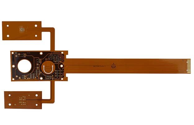
Below is an image of a 4 layer flex PCB of a shock-absorbing car seat to give you an idea of how four 4 layer flex PCB looks.
After a brief introduction, let us move on to another critical question of designing a 4 layer flex PCB and what things should be kept in mind while designing the four-layer printed circuit board as a beginner.

4 Layer Flex PCB
Things to Keep in Mind While Designing a 4 Layer Flex PCB?
The process of designing a flexible printed circuit board slightly differs from designing a hard or rigid circuit board.
Flexible or flex printed circuit boards are light in weight and can significantly save manufacturing costs. The design must be optimized for material and use cases.
There are five things to be kept in mind while designing a 4 layer flex PCB:
- Keep in mind the flexible electronic applications
Before starting the design of a 4 layer flex PCB, you need to be clear about how many times the printed circuit board will flex, the bend radius, and how thin or thick the printed circuit board should be. The application and type of boards should be known ahead of the designing process to answer these questions.
- The bend radius of your flexible printed circuit board
Bend radius is the amount of bendiness for the flex area, and it should be decided early in the design. The bend radius for a four-layer printed circuit board which falls in the category of multi-layer can be calculated using this diagram:
By deciding the bendability, you can determine the number of bends required in your design without damaging the Copper. One thing must be kept in mind that you should avoid 90-degree bends because they cause high strain. Also, the conductor smaller than ten mils should be placed in neutral bend areas with negligible strain.
- Know your flexible printed circuit board materials
In the flexible printed circuit boards, the materials have less dimensional stability than the rigid printed circuit boards. That is why flexible printed circuit boards require looser outline tolerance than any other board. You may require a hard tool or a laser cutting tool, depending on the profile tolerance. This requirement can increase the cost.
- The Flex Layers should be placed in the center of the Stack-up
The flex layers should be placed in the center of the stack-up. Placing the flex layers in the center protects them from the exposure of outer layer plating. This placement also improves the impedance, and the control in the flex area is also better when the flex layers are placed in the center of the stack-up. Another significant advantage in design for this placement is that it simplifies the manufacturing process.
- Keep an eye on Flex trace routing
The radius is kept large to increase the life span of the circuit. I-beaming is avoided because it causes stress which requires thinning the circuit to avoid breakage. Also, the traces should be kept curved instead of angled ones because it causes lower stress.
These were some of the general guidelines to design a 4 layer flex PCB. Now let us move on to the Layout of 4 layer flex PCBs.
Layout and Stack-up of 4 Layer Flex PCBs
The stack-up of 4 Layer Flex PCB is quite elaborate. There are two inner layers, layer one and layer two.
These two layers are sandwiched between the upper and bottom layers. A prepreg layer follows the top layer or signal layer.
Copper is used in the top layer. The prepreg layer is followed by the inner layer called the plane.
There is a core sublayer part of that inner layer. This layer is followed by inner layer two, which is a plane layer.
In the end, there is a final layer which is also a signal layer. Interconnects are soldered, and they are placed on the top and bottom layers.
In the layout portion, we should be familiar with the type of flex circuit types, including static and dynamic types.
Dynamic are those circuit which flexes regularly, and static circuits have minimal flexing.
Another important point to remember is pad size in a 4 layer flex PCB should be kept large to manage stress relief.
In the component placement of a four-layer flexible printed circuit board, you should keep in mind the X, Y, and Z spacing of components and the spacing in which the circuit is bent.
This is one of the significant differences in the Layout of rigid printed circuit boards and a four-layer flexible printed circuit board.
You can use three-dimensional flex printed circuit board design tools to keep track of the point where the circuit will bend. This will help you present a better layout.
4 Layer Flex PCB stackup
After the Layout and stack-up, we will discuss the major benefits of using four-layer flexible printed circuit boards.
What are the Benefits of 4 Layer Flex PCBs?
Although rigid printed circuit boards are mostly produced globally, having a flexible printed circuit board can have many unique advantages.
I am going to list some of the most important advantages for you here:
- 4 layer flex PCBs are compatible with almost any type of connector or component, and their compatibility is incomparable with other rigid printed circuit boards.
- The flexible circuit boards are relatively more stable and reliable than other rigid printed circuit boards. It is because flexible printed circuit boards have relatively fewer interconnects, and they have fewer solder joints than rigid printed circuit boards. It lessens the chances of faults and increases reliability.
- Also, the 4 layer flex PCBs are light in weight and reduce transportation costs. These kinds of circuit boards require only ten percent of common printed circuit boards’ space and weight. This provides greater freedom of installation, and the packaging process is also more manageable in the case of flexible printed circuit boards.
- 4 layer flex PCBs provide higher circuit density. This higher circuit density helps meet dynamic flexing requirements.
- These 4 layer flex PCBs have a wider temperature range. This helps operate in higher currents and improves the overall life of the electronic components.
- With improved signal quality, impedance control, and robust operating, four-layer printed circuit boards have the edge over other market options.

4 Layer Flex PCB
What are the Materials of 4 Layer Flex PCBs?
The material used in 4 layer flex PCB is of extreme importance because they guarantee the life of that product, and they should withstand the demands placed upon them.
We can categorize the material into three broad categories:
- Base material:
The base material is actually the material that provides the laminate foundation and is a flexible polymer film. In a 4 layer flex PCB, a polyimide film is used as a substrate.
It is because Polyimide does not soften when heated and stays flexible after thermosetting.
When adhesiveness flexible printed circuit boards are made, the base material actually displays all the basic characteristics.
Adhesiveness Polyimide attaches to Copper without an adhesive and lessens the thickness of the board. It provides more flexibility and a lower risk of breakage.
- Bonding Adhesive:
To create a laminate, we use adhesives as the bonding medium. If Polyimide is a base material, adhesive acts as a performance-limiting element of a laminate.
There are many problems associated with Polyimide adhesives. Newer thermoplastic Polyimide adhesives are suitable, but now adhesives from different Polymer families are used too.
Adhesive comes in different thicknesses, and their use depends upon the type of application in which the four-layer printed circuit board is going to be used. Their thickness is usually determined to fill the demands of Copper foil thickness.
- Metal Foil
In a flexible laminate, the conductive element is known as the metal foil. Circuit paths are usually engraved with metal foil.
A wide variety of metal foils are available in the market, but Copper foil is the most popular and accepted foil.
The electrical properties of Copper and cost-effectiveness with respect to other metals make it an automatic choice for the production of a four-layer printed circuit board.
There are two basic types of Copper foil: Wrought or rolled and electrodeposited. Both these types have different properties. The thin surface treatment is usually applied on Copper foil on one side to improve its adhesiveness to the base film.
Besides rolled and annealed foils, thinner electroplated films are also becoming a popular choice.

4 Layer Flex PCB
What is the Application of 4 layer flex PCBs?
4 layer flex PCBs have extensive applications ranging from the medical field to aeronautical to electronics.
Let us summarize the applications in few bullet points to give you an idea of how and where 4 layer flex PCBs are used:
- Flexible printed circuit boards are mainly used as connectors in different applications because of their inherent flexibility, easier maintenance, and less space-consuming ability.
- 4 layer flex PCBs are commonly used in computer keyboards. In keyboards, flexible printed circuit boards act as switching matrices.
- The automobiles industry widely uses flexible printed circuit boards. These boards are mainly used in under-hood control devices, dashboards, ABS systems, and circuits hidden in the cab roofs.
- 4 layer flex PCBs are used in consumer electronic devices like Cameras, calculators, personal entertainment devices, and motion monitors.
- Solar cells are powered by these 4 layer flex PCBs. Flexible printed circuit boards are used in these cells because they are lightweight and easily deployable. Also, flexible printed circuit boards can be sewn into backpacks or underwear too because they are lightweight.
- Medical and industrial products also use flexible printed circuit boards. They are mainly used as an interconnector of electrical components like integrated circuits, capacitors, and resistors.
- One last primary application of a 4 layer flex PCBis a cellular phone, commonly known as a cell phone. There are many interconnections required in a compact package in the cell phone. So, flexible printed circuit boards are used to complete the process with more efficiency.
Conclusion
By concluding this article, flexible printed circuit boards are the future.
With better and easier signal routing, improved EMI performance, and better efficiency, they can replace the rigid printed circuit boards currently in high demand. The coming era is of miniature designs and elegance.
4 layer flex PCBs have cost-effectiveness, elegance and can reduce electronic products’ size.
That is why the focus should be placed on flexible printed circuit boards to help technology make innovations in this field and overcame any technological flaws to use these flexible printed circuit boards in mass production.
Your Best 4 Layer Flex PCB Manufacturer in China
SMTFAB is a reliable 4 layer flex PCB supplier in China, and we can provide a one-stop solution for your project.
- Over 12 years 4 layer flex PCB manufacturing experience
- All 4 layer flex PCBs meet IPC Class 2 or 3
- 100% E-test and AOI inspection
- Offer a free sample before your mass production order
- 48h quick-turn service for your prototype 4 layer flex PCB
- 7/24 sales and engineering tech support
- Production Facility
- Flexible PCB Capabilities
- 4 Layer Flex PCB
For flexible PCB capabilities, please refer to the following form.
| Feature | Capability | |||||||
| Number of Layers | 1 – 10layers | |||||||
| Order Quantity | 1pc – 10000+pcs | |||||||
| Board thickness(without stiffener) | 0.002-0.2inch | |||||||
| Min. Board Size | 0.2*0.4inch | |||||||
| Min. Board Size | 9*14 inch | |||||||
| Build Time | 2days – 5weeks | |||||||
| Material | FCCL (adhesive) | Shengyi SF305 | ||||||
| FCCL (adhesiveness) | Panasonic R-F775 | |||||||
| Taiflex MHK | ||||||||
| Dupont Pyralux AP | ||||||||
| Coverlay | Shengyi SF305C | |||||||
| Taiflex FHK 1025&2035 | ||||||||
| Adhesive | Taiflex BT | |||||||
| PI stiffener | Taiflex MHK | |||||||
| 3M | 9077&6677&9058 | |||||||
| Others | Tolerance of single layer | ±0.05mm | ||||||
| Tolerance of double-layer (≤0.3mm) | ±0.05mm | |||||||
| Tolerance of multi-layer(<0.3mm) | ±0.05mm | |||||||
| Tolerance of multi-layer(0.3-0.8mm) | ±0.1mm | |||||||
| Impedance control tolerance | Single ended:±5Ω(≤50Ω);±10%(>50Ω) | |||||||
| Differential Pairs: ±5Ω (≤50Ω);±10%(>50Ω) | ||||||||
| Min coverlay bridge | 8mil | |||||||
| Min bend radius of single layer | 3-6 times of board thickness | |||||||
| Min bend radius of double-layer | 6-10 times of board thickness | |||||||
| Min bend radius of multilayer | 10-15 times of board thickness | |||||||
| Min dynamic bend radius | 20-40 times of board thickness | |||||||
| Inner layer | Min line width/spacing (12/18um copper) | 3.0/3.2mil (loop lines 6.0/6.2mil) | ||||||
| Min line width/spacing (35um copper) | 4.0/4.0mil (loop lines 8.0/8.0mil) | |||||||
| Min line width/spacing (70um copper) | 6.0/6.5mil (loop lines 10/10.5mil) | |||||||
| Max copper thickness | 2oz | |||||||
| Outer layer | Min line width/spacing (18um copper) | 3/3.2mil (loop lines 6/6mil) | ||||||
| Min line width/spacing (35um copper) | 4/4.5mil (loop lines 6/6mil) | |||||||
| Min line width/spacing (70um copper) | 6/7mil (loop lines 6/6mil) | |||||||
| Min line width/spacing (105um copper) | 10/13mil (loop lines 6/6mil) | |||||||
| Max finished copper thickness | 3OZ | |||||||
| Drilling | Min distance between via and conductors | 6mil (<4 layer) | ||||||
| 8mil (4-6 layer) | ||||||||
| 12mil (7-8 layer) | ||||||||
| Min mechanical drill hole | 6mil | |||||||
| Solder mask | Solder mask color | Green/White/Black/Yellow | ||||||
| and silkscreen | Coverlay | Yellow、Black | ||||||
| Min solder dam (base copper ≤ 1OZ) | 4mil (green),8mil(solder dam on the large copper) | |||||||
| Min clearance | 3mil (part for 2.5mil) | |||||||
| Silk color | White, Yellow | |||||||
| Surface treatment | Surface treatment | HASL, ENIG, ENEPIG, Electrolytic Nickel Gold, Soft gold, Hard gold, | ||||||
| Immersion silver and OSP | ||||||||
| Mixed surface treatment | ENIG+OSP, ENIG+G/F | |||||||
| Gold thickness (ENIG) | 0.05-0.10um | |||||||
| Nickel thickness (ENIG) | 3-6um | |||||||
| Gold thickness (ENEPIG) | 0.05-0.10um | |||||||
| Palladium thickness (ENEPIG) | 0.05-0.15um | |||||||
| Nick thickness (ENEPIG) | 3-6um | |||||||
| Electrolytic nickel thickness | 3-6um | |||||||
| Electrolytic gold thickness | 0.05-0.10um | |||||||
| Hard gold thickness (including lead) | 0.1-1.5um | |||||||
| OSP thickness | 0.1-0.3um | |||||||
| Immersion silver thickness | 0.2-0.4um | |||||||
| Routing | Laser accuracy | ±0.05mm | ||||||
| Punch accuracy | ±0.05mm–±0.15mm | |||||||
Please see the details of 4 Layer Flex PCB Stack-up as follows:
Related Some Other PCBs
Why Choose SMTFAB for Your 4 Layer Flex PCB
Flexible printed circuit boards(Flex PCBs) are now mainly used in the electronics industry. As one of the best manufacturers of flexible circuit boards, SMTFAB provides 4-layer flex PCBs for your projects.
What’s more, SMTFAB can offer a turnkey solution for your project. From PCB design & layout, PCB fabrication to PCB assembly, all processes are in-house and not outsourcing.
The quality is under our control, meanwhile, we can assure the delivery time even in the peak season.
These 4 layer flex PCBs have 4 conductive layers and the material is polyamide rather than FR4. The process of 4 layer flex PCB is also different from the 4 layer rigid PCB.
If you need your project very quickly, SMTFAB can help you. We can manufacture the sample of 4 layer flex PCB within 48h, it can meet your production schedule.
The standard board thickness of 4 layer flex PCB is 1/2mil to 3mil and the copper thickness is 1/3oz to 2oz.
We have full service for quick-turn jobs and state-of-the-art equipment. It can meet your complicated project deadlines and budgets.
There are many different applications for 4 layer flex PCB, such as power supply, medical device, automotive, industrial controls, smartphones, GPS systems, motion systems, and satellites.
4 Layer Flex PCB
Are you looking for a valuable 4 layer flex PCB supplier? SMTFAB is your best choice.
SMTFAB has over 500 workers in our workshop and the monthly capacity is 40,000 square meters.
We are here to support you when you have any questions about 4 layer flex PCB.
4 Layer Flex PCB: The Ultimate FAQ Guide
In the electronic industry, flexible printed circuit boards are used quite extensively. The use of these circuit boards ranges from industrial applications like power equipment, medical devices, automobile equipment, etc., to industrial control equipment.
A 4 layer flex PCB printed circuit board is one of the most widely used types of flexible printed circuit boards in the industry.
Let us start with the basic question that what actually is a four-layer flexible printed circuit board.
What is 4 Layer Flex PCB?
In flexible printed circuit boards, we assemble electronic circuits by mounting electrical devices on flexible plastic substrates.
Flexible circuit boards can also be screen-printed silver circuits on polyester.
There are four conductive layers in a 4 layer flex PCB, and the board is made up of Polyimide.
FR4 can also be used, but Polyimide is the best available option because it has numerous advantages over FR4.
Polyimide is a thermally stable material, and it allows four layers of a flexible printed circuit board to withstand higher temperatures.
That is why 4 layer flex PCBs are widely used in high-temperature applications.
Also, Polyimide offers considerable flexibility, making it easier to mount electronic devices that are otherwise difficult to mount on hard boards.
This helps streamlines the design. In addition to the above, Polyimide’s flexibility helps create an intricate design, which is impossible with the rigid circuit board.
Polyimide helps in reducing the overall weight of printed circuit boards too.
Below is an image of a 4 layer flex PCB of a shock-absorbing car seat to give you an idea of how four 4 layer flex PCB looks.
After a brief introduction, let us move on to another critical question of designing a 4 layer flex PCB and what things should be kept in mind while designing the four-layer printed circuit board as a beginner.
4 Layer Flex PCB
Things to Keep in Mind While Designing a 4 Layer Flex PCB?
The process of designing a flexible printed circuit board slightly differs from designing a hard or rigid circuit board.
Flexible or flex printed circuit boards are light in weight and can significantly save manufacturing costs. The design must be optimized for material and use cases.
There are five things to be kept in mind while designing a 4 layer flex PCB:
- Keep in mind the flexible electronic applications
Before starting the design of a 4 layer flex PCB, you need to be clear about how many times the printed circuit board will flex, the bend radius, and how thin or thick the printed circuit board should be. The application and type of boards should be known ahead of the designing process to answer these questions.
- The bend radius of your flexible printed circuit board
Bend radius is the amount of bendiness for the flex area, and it should be decided early in the design. The bend radius for a four-layer printed circuit board which falls in the category of multi-layer can be calculated using this diagram:
By deciding the bendability, you can determine the number of bends required in your design without damaging the Copper. One thing must be kept in mind that you should avoid 90-degree bends because they cause high strain. Also, the conductor smaller than ten mils should be placed in neutral bend areas with negligible strain.
- Know your flexible printed circuit board materials
In the flexible printed circuit boards, the materials have less dimensional stability than the rigid printed circuit boards. That is why flexible printed circuit boards require looser outline tolerance than any other board. You may require a hard tool or a laser cutting tool, depending on the profile tolerance. This requirement can increase the cost.
- The Flex Layers should be placed in the center of the Stack-up
The flex layers should be placed in the center of the stack-up. Placing the flex layers in the center protects them from the exposure of outer layer plating. This placement also improves the impedance, and the control in the flex area is also better when the flex layers are placed in the center of the stack-up. Another significant advantage in design for this placement is that it simplifies the manufacturing process.
- Keep an eye on Flex trace routing
The radius is kept large to increase the life span of the circuit. I-beaming is avoided because it causes stress which requires thinning the circuit to avoid breakage. Also, the traces should be kept curved instead of angled ones because it causes lower stress.
These were some of the general guidelines to design a 4 layer flex PCB. Now let us move on to the Layout of 4 layer flex PCBs.
Layout and Stack-up of 4 Layer Flex PCBs
The stack-up of 4 Layer Flex PCB is quite elaborate. There are two inner layers, layer one and layer two.
These two layers are sandwiched between the upper and bottom layers. A prepreg layer follows the top layer or signal layer.
Copper is used in the top layer. The prepreg layer is followed by the inner layer called the plane.
There is a core sublayer part of that inner layer. This layer is followed by inner layer two, which is a plane layer.
In the end, there is a final layer which is also a signal layer. Interconnects are soldered, and they are placed on the top and bottom layers.
In the layout portion, we should be familiar with the type of flex circuit types, including static and dynamic types.
Dynamic are those circuit which flexes regularly, and static circuits have minimal flexing.
Another important point to remember is pad size in a 4 layer flex PCB should be kept large to manage stress relief.
In the component placement of a four-layer flexible printed circuit board, you should keep in mind the X, Y, and Z spacing of components and the spacing in which the circuit is bent.
This is one of the significant differences in the Layout of rigid printed circuit boards and a four-layer flexible printed circuit board.
You can use three-dimensional flex printed circuit board design tools to keep track of the point where the circuit will bend. This will help you present a better layout.
4 Layer Flex PCB stackup
After the Layout and stack-up, we will discuss the major benefits of using four-layer flexible printed circuit boards.
What are the Benefits of 4 Layer Flex PCBs?
Although rigid printed circuit boards are mostly produced globally, having a flexible printed circuit board can have many unique advantages.
I am going to list some of the most important advantages for you here:
- 4 layer flex PCBs are compatible with almost any type of connector or component, and their compatibility is incomparable with other rigid printed circuit boards.
- The flexible circuit boards are relatively more stable and reliable than other rigid printed circuit boards. It is because flexible printed circuit boards have relatively fewer interconnects, and they have fewer solder joints than rigid printed circuit boards. It lessens the chances of faults and increases reliability.
- Also, the 4 layer flex PCBs are light in weight and reduce transportation costs. These kinds of circuit boards require only ten percent of common printed circuit boards’ space and weight. This provides greater freedom of installation, and the packaging process is also more manageable in the case of flexible printed circuit boards.
- 4 layer flex PCBs provide higher circuit density. This higher circuit density helps meet dynamic flexing requirements.
- These 4 layer flex PCBs have a wider temperature range. This helps operate in higher currents and improves the overall life of the electronic components.
- With improved signal quality, impedance control, and robust operating, four-layer printed circuit boards have the edge over other market options.
4 Layer Flex PCB
What are the Materials of 4 Layer Flex PCBs?
The material used in 4 layer flex PCB is of extreme importance because they guarantee the life of that product, and they should withstand the demands placed upon them.
We can categorize the material into three broad categories:
- Base material:
The base material is actually the material that provides the laminate foundation and is a flexible polymer film. In a 4 layer flex PCB, a polyimide film is used as a substrate.
It is because Polyimide does not soften when heated and stays flexible after thermosetting.
When adhesiveness flexible printed circuit boards are made, the base material actually displays all the basic characteristics.
Adhesiveness Polyimide attaches to Copper without an adhesive and lessens the thickness of the board. It provides more flexibility and a lower risk of breakage.
- Bonding Adhesive:
To create a laminate, we use adhesives as the bonding medium. If Polyimide is a base material, adhesive acts as a performance-limiting element of a laminate.
There are many problems associated with Polyimide adhesives. Newer thermoplastic Polyimide adhesives are suitable, but now adhesives from different Polymer families are used too.
Adhesive comes in different thicknesses, and their use depends upon the type of application in which the four-layer printed circuit board is going to be used. Their thickness is usually determined to fill the demands of Copper foil thickness.
- Metal Foil
In a flexible laminate, the conductive element is known as the metal foil. Circuit paths are usually engraved with metal foil.
A wide variety of metal foils are available in the market, but Copper foil is the most popular and accepted foil.
The electrical properties of Copper and cost-effectiveness with respect to other metals make it an automatic choice for the production of a four-layer printed circuit board.
There are two basic types of Copper foil: Wrought or rolled and electrodeposited. Both these types have different properties. The thin surface treatment is usually applied on Copper foil on one side to improve its adhesiveness to the base film.
Besides rolled and annealed foils, thinner electroplated films are also becoming a popular choice.
4 Layer Flex PCB
What is the Application of 4 layer flex PCBs?
4 layer flex PCBs have extensive applications ranging from the medical field to aeronautical to electronics.
Let us summarize the applications in few bullet points to give you an idea of how and where 4 layer flex PCBs are used:
- Flexible printed circuit boards are mainly used as connectors in different applications because of their inherent flexibility, easier maintenance, and less space-consuming ability.
- 4 layer flex PCBs are commonly used in computer keyboards. In keyboards, flexible printed circuit boards act as switching matrices.
- The automobiles industry widely uses flexible printed circuit boards. These boards are mainly used in under-hood control devices, dashboards, ABS systems, and circuits hidden in the cab roofs.
- 4 layer flex PCBs are used in consumer electronic devices like Cameras, calculators, personal entertainment devices, and motion monitors.
- Solar cells are powered by these 4 layer flex PCBs. Flexible printed circuit boards are used in these cells because they are lightweight and easily deployable. Also, flexible printed circuit boards can be sewn into backpacks or underwear too because they are lightweight.
- Medical and industrial products also use flexible printed circuit boards. They are mainly used as an interconnector of electrical components like integrated circuits, capacitors, and resistors.
- One last primary application of a 4 layer flex PCBis a cellular phone, commonly known as a cell phone. There are many interconnections required in a compact package in the cell phone. So, flexible printed circuit boards are used to complete the process with more efficiency.
Conclusion
By concluding this article, flexible printed circuit boards are the future.
With better and easier signal routing, improved EMI performance, and better efficiency, they can replace the rigid printed circuit boards currently in high demand. The coming era is of miniature designs and elegance.
4 layer flex PCBs have cost-effectiveness, elegance and can reduce electronic products’ size.
That is why the focus should be placed on flexible printed circuit boards to help technology make innovations in this field and overcame any technological flaws to use these flexible printed circuit boards in mass production.
Your Best 4 Layer Flex PCB Manufacturer in China
SMTFAB is a reliable 4 layer flex PCB supplier in China, and we can provide a one-stop solution for your project.
- Over 12 years 4 layer flex PCB manufacturing experience
- All 4 layer flex PCBs meet IPC Class 2 or 3
- 100% E-test and AOI inspection
- Offer a free sample before your mass production order
- 48h quick-turn service for your prototype 4 layer flex PCB
- 7/24 sales and engineering tech support
Your Best 4 Layer Flex PCB Manufacturer in China
Your Best 4 Layer Flex PCB Manufacturer in China
SMTFAB is a reliable 4 layer flex PCB supplier in China, and we can provide a one-stop solution for your project.
- Over 12 years 4 layer flex PCB manufacturing experience
- All 4 layer flex PCBs meet IPC Class 2 or 3
- 100% E-test and AOI inspection
- Offer a free sample before your mass production order
- 48h quick-turn service for your prototype 4 layer flex PCB
- 7/24 sales and engineering tech support
- Production Facility
- Flexible PCB Capabilities
- 4 Layer Flex PCB
For flexible PCB capabilities, please refer to the following form.
| Feature | Capability | |||||||
| Number of Layers | 1 – 10layers | |||||||
| Order Quantity | 1pc – 10000+pcs | |||||||
| Board thickness(without stiffener) | 0.002-0.2inch | |||||||
| Min. Board Size | 0.2*0.4inch | |||||||
| Min. Board Size | 9*14 inch | |||||||
| Build Time | 2days – 5weeks | |||||||
| Material | FCCL (adhesive) | Shengyi SF305 | ||||||
| FCCL (adhesiveness) | Panasonic R-F775 | |||||||
| Taiflex MHK | ||||||||
| Dupont Pyralux AP | ||||||||
| Coverlay | Shengyi SF305C | |||||||
| Taiflex FHK 1025&2035 | ||||||||
| Adhesive | Taiflex BT | |||||||
| PI stiffener | Taiflex MHK | |||||||
| 3M | 9077&6677&9058 | |||||||
| Others | Tolerance of single layer | ±0.05mm | ||||||
| Tolerance of double-layer (≤0.3mm) | ±0.05mm | |||||||
| Tolerance of multi-layer(<0.3mm) | ±0.05mm | |||||||
| Tolerance of multi-layer(0.3-0.8mm) | ±0.1mm | |||||||
| Impedance control tolerance | Single ended:±5Ω(≤50Ω);±10%(>50Ω) | |||||||
| Differential Pairs: ±5Ω (≤50Ω);±10%(>50Ω) | ||||||||
| Min coverlay bridge | 8mil | |||||||
| Min bend radius of single layer | 3-6 times of board thickness | |||||||
| Min bend radius of double-layer | 6-10 times of board thickness | |||||||
| Min bend radius of multilayer | 10-15 times of board thickness | |||||||
| Min dynamic bend radius | 20-40 times of board thickness | |||||||
| Inner layer | Min line width/spacing (12/18um copper) | 3.0/3.2mil (loop lines 6.0/6.2mil) | ||||||
| Min line width/spacing (35um copper) | 4.0/4.0mil (loop lines 8.0/8.0mil) | |||||||
| Min line width/spacing (70um copper) | 6.0/6.5mil (loop lines 10/10.5mil) | |||||||
| Max copper thickness | 2oz | |||||||
| Outer layer | Min line width/spacing (18um copper) | 3/3.2mil (loop lines 6/6mil) | ||||||
| Min line width/spacing (35um copper) | 4/4.5mil (loop lines 6/6mil) | |||||||
| Min line width/spacing (70um copper) | 6/7mil (loop lines 6/6mil) | |||||||
| Min line width/spacing (105um copper) | 10/13mil (loop lines 6/6mil) | |||||||
| Max finished copper thickness | 3OZ | |||||||
| Drilling | Min distance between via and conductors | 6mil (<4 layer) | ||||||
| 8mil (4-6 layer) | ||||||||
| 12mil (7-8 layer) | ||||||||
| Min mechanical drill hole | 6mil | |||||||
| Solder mask | Solder mask color | Green/White/Black/Yellow | ||||||
| and silkscreen | Coverlay | Yellow、Black | ||||||
| Min solder dam (base copper ≤ 1OZ) | 4mil (green),8mil(solder dam on the large copper) | |||||||
| Min clearance | 3mil (part for 2.5mil) | |||||||
| Silk color | White, Yellow | |||||||
| Surface treatment | Surface treatment | HASL, ENIG, ENEPIG, Electrolytic Nickel Gold, Soft gold, Hard gold, | ||||||
| Immersion silver and OSP | ||||||||
| Mixed surface treatment | ENIG+OSP, ENIG+G/F | |||||||
| Gold thickness (ENIG) | 0.05-0.10um | |||||||
| Nickel thickness (ENIG) | 3-6um | |||||||
| Gold thickness (ENEPIG) | 0.05-0.10um | |||||||
| Palladium thickness (ENEPIG) | 0.05-0.15um | |||||||
| Nick thickness (ENEPIG) | 3-6um | |||||||
| Electrolytic nickel thickness | 3-6um | |||||||
| Electrolytic gold thickness | 0.05-0.10um | |||||||
| Hard gold thickness (including lead) | 0.1-1.5um | |||||||
| OSP thickness | 0.1-0.3um | |||||||
| Immersion silver thickness | 0.2-0.4um | |||||||
| Routing | Laser accuracy | ±0.05mm | ||||||
| Punch accuracy | ±0.05mm–±0.15mm | |||||||
Please see the details of 4 Layer Flex PCB Stack-up as follows:
- Production Facility
- Flexible PCB Capabilities
- 4 Layer Flex PCB
For flexible PCB capabilities, please refer to the following form.
| Feature | Capability | |||||||
| Number of Layers | 1 – 10layers | |||||||
| Order Quantity | 1pc – 10000+pcs | |||||||
| Board thickness(without stiffener) | 0.002-0.2inch | |||||||
| Min. Board Size | 0.2*0.4inch | |||||||
| Min. Board Size | 9*14 inch | |||||||
| Build Time | 2days – 5weeks | |||||||
| Material | FCCL (adhesive) | Shengyi SF305 | ||||||
| FCCL (adhesiveness) | Panasonic R-F775 | |||||||
| Taiflex MHK | ||||||||
| Dupont Pyralux AP | ||||||||
| Coverlay | Shengyi SF305C | |||||||
| Taiflex FHK 1025&2035 | ||||||||
| Adhesive | Taiflex BT | |||||||
| PI stiffener | Taiflex MHK | |||||||
| 3M | 9077&6677&9058 | |||||||
| Others | Tolerance of single layer | ±0.05mm | ||||||
| Tolerance of double-layer (≤0.3mm) | ±0.05mm | |||||||
| Tolerance of multi-layer(<0.3mm) | ±0.05mm | |||||||
| Tolerance of multi-layer(0.3-0.8mm) | ±0.1mm | |||||||
| Impedance control tolerance | Single ended:±5Ω(≤50Ω);±10%(>50Ω) | |||||||
| Differential Pairs: ±5Ω (≤50Ω);±10%(>50Ω) | ||||||||
| Min coverlay bridge | 8mil | |||||||
| Min bend radius of single layer | 3-6 times of board thickness | |||||||
| Min bend radius of double-layer | 6-10 times of board thickness | |||||||
| Min bend radius of multilayer | 10-15 times of board thickness | |||||||
| Min dynamic bend radius | 20-40 times of board thickness | |||||||
| Inner layer | Min line width/spacing (12/18um copper) | 3.0/3.2mil (loop lines 6.0/6.2mil) | ||||||
| Min line width/spacing (35um copper) | 4.0/4.0mil (loop lines 8.0/8.0mil) | |||||||
| Min line width/spacing (70um copper) | 6.0/6.5mil (loop lines 10/10.5mil) | |||||||
| Max copper thickness | 2oz | |||||||
| Outer layer | Min line width/spacing (18um copper) | 3/3.2mil (loop lines 6/6mil) | ||||||
| Min line width/spacing (35um copper) | 4/4.5mil (loop lines 6/6mil) | |||||||
| Min line width/spacing (70um copper) | 6/7mil (loop lines 6/6mil) | |||||||
| Min line width/spacing (105um copper) | 10/13mil (loop lines 6/6mil) | |||||||
| Max finished copper thickness | 3OZ | |||||||
| Drilling | Min distance between via and conductors | 6mil (<4 layer) | ||||||
| 8mil (4-6 layer) | ||||||||
| 12mil (7-8 layer) | ||||||||
| Min mechanical drill hole | 6mil | |||||||
| Solder mask | Solder mask color | Green/White/Black/Yellow | ||||||
| and silkscreen | Coverlay | Yellow、Black | ||||||
| Min solder dam (base copper ≤ 1OZ) | 4mil (green),8mil(solder dam on the large copper) | |||||||
| Min clearance | 3mil (part for 2.5mil) | |||||||
| Silk color | White, Yellow | |||||||
| Surface treatment | Surface treatment | HASL, ENIG, ENEPIG, Electrolytic Nickel Gold, Soft gold, Hard gold, | ||||||
| Immersion silver and OSP | ||||||||
| Mixed surface treatment | ENIG+OSP, ENIG+G/F | |||||||
| Gold thickness (ENIG) | 0.05-0.10um | |||||||
| Nickel thickness (ENIG) | 3-6um | |||||||
| Gold thickness (ENEPIG) | 0.05-0.10um | |||||||
| Palladium thickness (ENEPIG) | 0.05-0.15um | |||||||
| Nick thickness (ENEPIG) | 3-6um | |||||||
| Electrolytic nickel thickness | 3-6um | |||||||
| Electrolytic gold thickness | 0.05-0.10um | |||||||
| Hard gold thickness (including lead) | 0.1-1.5um | |||||||
| OSP thickness | 0.1-0.3um | |||||||
| Immersion silver thickness | 0.2-0.4um | |||||||
| Routing | Laser accuracy | ±0.05mm | ||||||
| Punch accuracy | ±0.05mm–±0.15mm | |||||||
Please see the details of 4 Layer Flex PCB Stack-up as follows:
Please see the details of 4 Layer Flex PCB Stack-up as follows:
Related Some Other PCBs
Related Some Other PCBs
Why Choose SMTFAB for Your 4 Layer Flex PCB
Flexible printed circuit boards(Flex PCBs) are now mainly used in the electronics industry. As one of the best manufacturers of flexible circuit boards, SMTFAB provides 4-layer flex PCBs for your projects.
What’s more, SMTFAB can offer a turnkey solution for your project. From PCB design & layout, PCB fabrication to PCB assembly, all processes are in-house and not outsourcing.
The quality is under our control, meanwhile, we can assure the delivery time even in the peak season.
These 4 layer flex PCBs have 4 conductive layers and the material is polyamide rather than FR4. The process of 4 layer flex PCB is also different from the 4 layer rigid PCB.
If you need your project very quickly, SMTFAB can help you. We can manufacture the sample of 4 layer flex PCB within 48h, it can meet your production schedule.
The standard board thickness of 4 layer flex PCB is 1/2mil to 3mil and the copper thickness is 1/3oz to 2oz.
We have full service for quick-turn jobs and state-of-the-art equipment. It can meet your complicated project deadlines and budgets.
There are many different applications for 4 layer flex PCB, such as power supply, medical device, automotive, industrial controls, smartphones, GPS systems, motion systems, and satellites.
4 Layer Flex PCB
Are you looking for a valuable 4 layer flex PCB supplier? SMTFAB is your best choice.
SMTFAB has over 500 workers in our workshop and the monthly capacity is 40,000 square meters.
We are here to support you when you have any questions about 4 layer flex PCB.
4 Layer Flex PCB: The Ultimate FAQ Guide
In the electronic industry, flexible printed circuit boards are used quite extensively. The use of these circuit boards ranges from industrial applications like power equipment, medical devices, automobile equipment, etc., to industrial control equipment.
A 4 layer flex PCB printed circuit board is one of the most widely used types of flexible printed circuit boards in the industry.
Let us start with the basic question that what actually is a four-layer flexible printed circuit board.
What is 4 Layer Flex PCB?
In flexible printed circuit boards, we assemble electronic circuits by mounting electrical devices on flexible plastic substrates.
Flexible circuit boards can also be screen-printed silver circuits on polyester.
There are four conductive layers in a 4 layer flex PCB, and the board is made up of Polyimide.
FR4 can also be used, but Polyimide is the best available option because it has numerous advantages over FR4.
Polyimide is a thermally stable material, and it allows four layers of a flexible printed circuit board to withstand higher temperatures.
That is why 4 layer flex PCBs are widely used in high-temperature applications.
Also, Polyimide offers considerable flexibility, making it easier to mount electronic devices that are otherwise difficult to mount on hard boards.
This helps streamlines the design. In addition to the above, Polyimide’s flexibility helps create an intricate design, which is impossible with the rigid circuit board.
Polyimide helps in reducing the overall weight of printed circuit boards too.
Below is an image of a 4 layer flex PCB of a shock-absorbing car seat to give you an idea of how four 4 layer flex PCB looks.
After a brief introduction, let us move on to another critical question of designing a 4 layer flex PCB and what things should be kept in mind while designing the four-layer printed circuit board as a beginner.
4 Layer Flex PCB
Things to Keep in Mind While Designing a 4 Layer Flex PCB?
The process of designing a flexible printed circuit board slightly differs from designing a hard or rigid circuit board.
Flexible or flex printed circuit boards are light in weight and can significantly save manufacturing costs. The design must be optimized for material and use cases.
There are five things to be kept in mind while designing a 4 layer flex PCB:
- Keep in mind the flexible electronic applications
Before starting the design of a 4 layer flex PCB, you need to be clear about how many times the printed circuit board will flex, the bend radius, and how thin or thick the printed circuit board should be. The application and type of boards should be known ahead of the designing process to answer these questions.
- The bend radius of your flexible printed circuit board
Bend radius is the amount of bendiness for the flex area, and it should be decided early in the design. The bend radius for a four-layer printed circuit board which falls in the category of multi-layer can be calculated using this diagram:
By deciding the bendability, you can determine the number of bends required in your design without damaging the Copper. One thing must be kept in mind that you should avoid 90-degree bends because they cause high strain. Also, the conductor smaller than ten mils should be placed in neutral bend areas with negligible strain.
- Know your flexible printed circuit board materials
In the flexible printed circuit boards, the materials have less dimensional stability than the rigid printed circuit boards. That is why flexible printed circuit boards require looser outline tolerance than any other board. You may require a hard tool or a laser cutting tool, depending on the profile tolerance. This requirement can increase the cost.
- The Flex Layers should be placed in the center of the Stack-up
The flex layers should be placed in the center of the stack-up. Placing the flex layers in the center protects them from the exposure of outer layer plating. This placement also improves the impedance, and the control in the flex area is also better when the flex layers are placed in the center of the stack-up. Another significant advantage in design for this placement is that it simplifies the manufacturing process.
- Keep an eye on Flex trace routing
The radius is kept large to increase the life span of the circuit. I-beaming is avoided because it causes stress which requires thinning the circuit to avoid breakage. Also, the traces should be kept curved instead of angled ones because it causes lower stress.
These were some of the general guidelines to design a 4 layer flex PCB. Now let us move on to the Layout of 4 layer flex PCBs.
Layout and Stack-up of 4 Layer Flex PCBs
The stack-up of 4 Layer Flex PCB is quite elaborate. There are two inner layers, layer one and layer two.
These two layers are sandwiched between the upper and bottom layers. A prepreg layer follows the top layer or signal layer.
Copper is used in the top layer. The prepreg layer is followed by the inner layer called the plane.
There is a core sublayer part of that inner layer. This layer is followed by inner layer two, which is a plane layer.
In the end, there is a final layer which is also a signal layer. Interconnects are soldered, and they are placed on the top and bottom layers.
In the layout portion, we should be familiar with the type of flex circuit types, including static and dynamic types.
Dynamic are those circuit which flexes regularly, and static circuits have minimal flexing.
Another important point to remember is pad size in a 4 layer flex PCB should be kept large to manage stress relief.
In the component placement of a four-layer flexible printed circuit board, you should keep in mind the X, Y, and Z spacing of components and the spacing in which the circuit is bent.
This is one of the significant differences in the Layout of rigid printed circuit boards and a four-layer flexible printed circuit board.
You can use three-dimensional flex printed circuit board design tools to keep track of the point where the circuit will bend. This will help you present a better layout.
4 Layer Flex PCB stackup
After the Layout and stack-up, we will discuss the major benefits of using four-layer flexible printed circuit boards.
What are the Benefits of 4 Layer Flex PCBs?
Although rigid printed circuit boards are mostly produced globally, having a flexible printed circuit board can have many unique advantages.
I am going to list some of the most important advantages for you here:
- 4 layer flex PCBs are compatible with almost any type of connector or component, and their compatibility is incomparable with other rigid printed circuit boards.
- The flexible circuit boards are relatively more stable and reliable than other rigid printed circuit boards. It is because flexible printed circuit boards have relatively fewer interconnects, and they have fewer solder joints than rigid printed circuit boards. It lessens the chances of faults and increases reliability.
- Also, the 4 layer flex PCBs are light in weight and reduce transportation costs. These kinds of circuit boards require only ten percent of common printed circuit boards’ space and weight. This provides greater freedom of installation, and the packaging process is also more manageable in the case of flexible printed circuit boards.
- 4 layer flex PCBs provide higher circuit density. This higher circuit density helps meet dynamic flexing requirements.
- These 4 layer flex PCBs have a wider temperature range. This helps operate in higher currents and improves the overall life of the electronic components.
- With improved signal quality, impedance control, and robust operating, four-layer printed circuit boards have the edge over other market options.
4 Layer Flex PCB
What are the Materials of 4 Layer Flex PCBs?
The material used in 4 layer flex PCB is of extreme importance because they guarantee the life of that product, and they should withstand the demands placed upon them.
We can categorize the material into three broad categories:
- Base material:
The base material is actually the material that provides the laminate foundation and is a flexible polymer film. In a 4 layer flex PCB, a polyimide film is used as a substrate.
It is because Polyimide does not soften when heated and stays flexible after thermosetting.
When adhesiveness flexible printed circuit boards are made, the base material actually displays all the basic characteristics.
Adhesiveness Polyimide attaches to Copper without an adhesive and lessens the thickness of the board. It provides more flexibility and a lower risk of breakage.
- Bonding Adhesive:
To create a laminate, we use adhesives as the bonding medium. If Polyimide is a base material, adhesive acts as a performance-limiting element of a laminate.
There are many problems associated with Polyimide adhesives. Newer thermoplastic Polyimide adhesives are suitable, but now adhesives from different Polymer families are used too.
Adhesive comes in different thicknesses, and their use depends upon the type of application in which the four-layer printed circuit board is going to be used. Their thickness is usually determined to fill the demands of Copper foil thickness.
- Metal Foil
In a flexible laminate, the conductive element is known as the metal foil. Circuit paths are usually engraved with metal foil.
A wide variety of metal foils are available in the market, but Copper foil is the most popular and accepted foil.
The electrical properties of Copper and cost-effectiveness with respect to other metals make it an automatic choice for the production of a four-layer printed circuit board.
There are two basic types of Copper foil: Wrought or rolled and electrodeposited. Both these types have different properties. The thin surface treatment is usually applied on Copper foil on one side to improve its adhesiveness to the base film.
Besides rolled and annealed foils, thinner electroplated films are also becoming a popular choice.
4 Layer Flex PCB
What is the Application of 4 layer flex PCBs?
4 layer flex PCBs have extensive applications ranging from the medical field to aeronautical to electronics.
Let us summarize the applications in few bullet points to give you an idea of how and where 4 layer flex PCBs are used:
- Flexible printed circuit boards are mainly used as connectors in different applications because of their inherent flexibility, easier maintenance, and less space-consuming ability.
- 4 layer flex PCBs are commonly used in computer keyboards. In keyboards, flexible printed circuit boards act as switching matrices.
- The automobiles industry widely uses flexible printed circuit boards. These boards are mainly used in under-hood control devices, dashboards, ABS systems, and circuits hidden in the cab roofs.
- 4 layer flex PCBs are used in consumer electronic devices like Cameras, calculators, personal entertainment devices, and motion monitors.
- Solar cells are powered by these 4 layer flex PCBs. Flexible printed circuit boards are used in these cells because they are lightweight and easily deployable. Also, flexible printed circuit boards can be sewn into backpacks or underwear too because they are lightweight.
- Medical and industrial products also use flexible printed circuit boards. They are mainly used as an interconnector of electrical components like integrated circuits, capacitors, and resistors.
- One last primary application of a 4 layer flex PCBis a cellular phone, commonly known as a cell phone. There are many interconnections required in a compact package in the cell phone. So, flexible printed circuit boards are used to complete the process with more efficiency.
Conclusion
By concluding this article, flexible printed circuit boards are the future.
With better and easier signal routing, improved EMI performance, and better efficiency, they can replace the rigid printed circuit boards currently in high demand. The coming era is of miniature designs and elegance.
4 layer flex PCBs have cost-effectiveness, elegance and can reduce electronic products’ size.
That is why the focus should be placed on flexible printed circuit boards to help technology make innovations in this field and overcame any technological flaws to use these flexible printed circuit boards in mass production.
Why Choose SMTFAB for Your 4 Layer Flex PCB
Flexible printed circuit boards(Flex PCBs) are now mainly used in the electronics industry. As one of the best manufacturers of flexible circuit boards, SMTFAB provides 4-layer flex PCBs for your projects.
What’s more, SMTFAB can offer a turnkey solution for your project. From PCB design & layout, PCB fabrication to PCB assembly, all processes are in-house and not outsourcing.
The quality is under our control, meanwhile, we can assure the delivery time even in the peak season.
These 4 layer flex PCBs have 4 conductive layers and the material is polyamide rather than FR4. The process of 4 layer flex PCB is also different from the 4 layer rigid PCB.
If you need your project very quickly, SMTFAB can help you. We can manufacture the sample of 4 layer flex PCB within 48h, it can meet your production schedule.
The standard board thickness of 4 layer flex PCB is 1/2mil to 3mil and the copper thickness is 1/3oz to 2oz.
We have full service for quick-turn jobs and state-of-the-art equipment. It can meet your complicated project deadlines and budgets.
There are many different applications for 4 layer flex PCB, such as power supply, medical device, automotive, industrial controls, smartphones, GPS systems, motion systems, and satellites.
Are you looking for a valuable 4 layer flex PCB supplier? SMTFAB is your best choice.
SMTFAB has over 500 workers in our workshop and the monthly capacity is 40,000 square meters.
We are here to support you when you have any questions about 4 layer flex PCB.
4 Layer Flex PCB: The Ultimate FAQ Guide
In the electronic industry, flexible printed circuit boards are used quite extensively. The use of these circuit boards ranges from industrial applications like power equipment, medical devices, automobile equipment, etc., to industrial control equipment.
A 4 layer flex PCB printed circuit board is one of the most widely used types of flexible printed circuit boards in the industry.
Let us start with the basic question that what actually is a four-layer flexible printed circuit board.
- What is 4 Layer Flex PCB?
- Things to Keep in Mind While Designing a 4 Layer Flex PCB
- Layout and Stack-up of 4 Layer Flex PCB
- What are the Benefits of 4 Layer Flex PCBs?
- What are the Materials of 4 Layer Flex PCBs?
- What is the Application of 4 layer flex PCBs?
- Conclusion
What is 4 Layer Flex PCB?
In flexible printed circuit boards, we assemble electronic circuits by mounting electrical devices on flexible plastic substrates.
Flexible circuit boards can also be screen-printed silver circuits on polyester.
There are four conductive layers in a 4 layer flex PCB, and the board is made up of Polyimide.
FR4 can also be used, but Polyimide is the best available option because it has numerous advantages over FR4.
Polyimide is a thermally stable material, and it allows four layers of a flexible printed circuit board to withstand higher temperatures.
That is why 4 layer flex PCBs are widely used in high-temperature applications.
Also, Polyimide offers considerable flexibility, making it easier to mount electronic devices that are otherwise difficult to mount on hard boards.
This helps streamlines the design. In addition to the above, Polyimide’s flexibility helps create an intricate design, which is impossible with the rigid circuit board.
Polyimide helps in reducing the overall weight of printed circuit boards too.
Below is an image of a 4 layer flex PCB of a shock-absorbing car seat to give you an idea of how four 4 layer flex PCB looks.
After a brief introduction, let us move on to another critical question of designing a 4 layer flex PCB and what things should be kept in mind while designing the four-layer printed circuit board as a beginner.
Things to Keep in Mind While Designing a 4 Layer Flex PCB?
The process of designing a flexible printed circuit board slightly differs from designing a hard or rigid circuit board.
Flexible or flex printed circuit boards are light in weight and can significantly save manufacturing costs. The design must be optimized for material and use cases.
There are five things to be kept in mind while designing a 4 layer flex PCB:
- Keep in mind the flexible electronic applications
Before starting the design of a 4 layer flex PCB, you need to be clear about how many times the printed circuit board will flex, the bend radius, and how thin or thick the printed circuit board should be. The application and type of boards should be known ahead of the designing process to answer these questions.
- The bend radius of your flexible printed circuit board
Bend radius is the amount of bendiness for the flex area, and it should be decided early in the design. The bend radius for a four-layer printed circuit board which falls in the category of multi-layer can be calculated using this diagram:
By deciding the bendability, you can determine the number of bends required in your design without damaging the Copper. One thing must be kept in mind that you should avoid 90-degree bends because they cause high strain. Also, the conductor smaller than ten mils should be placed in neutral bend areas with negligible strain.
- Know your flexible printed circuit board materials
In the flexible printed circuit boards, the materials have less dimensional stability than the rigid printed circuit boards. That is why flexible printed circuit boards require looser outline tolerance than any other board. You may require a hard tool or a laser cutting tool, depending on the profile tolerance. This requirement can increase the cost.
- The Flex Layers should be placed in the center of the Stack-up
The flex layers should be placed in the center of the stack-up. Placing the flex layers in the center protects them from the exposure of outer layer plating. This placement also improves the impedance, and the control in the flex area is also better when the flex layers are placed in the center of the stack-up. Another significant advantage in design for this placement is that it simplifies the manufacturing process.
- Keep an eye on Flex trace routing
The radius is kept large to increase the life span of the circuit. I-beaming is avoided because it causes stress which requires thinning the circuit to avoid breakage. Also, the traces should be kept curved instead of angled ones because it causes lower stress.
These were some of the general guidelines to design a 4 layer flex PCB. Now let us move on to the Layout of 4 layer flex PCBs.
Layout and Stack-up of 4 Layer Flex PCBs
The stack-up of 4 Layer Flex PCB is quite elaborate. There are two inner layers, layer one and layer two.
These two layers are sandwiched between the upper and bottom layers. A prepreg layer follows the top layer or signal layer.
Copper is used in the top layer. The prepreg layer is followed by the inner layer called the plane.
There is a core sublayer part of that inner layer. This layer is followed by inner layer two, which is a plane layer.
In the end, there is a final layer which is also a signal layer. Interconnects are soldered, and they are placed on the top and bottom layers.
In the layout portion, we should be familiar with the type of flex circuit types, including static and dynamic types.
Dynamic are those circuit which flexes regularly, and static circuits have minimal flexing.
Another important point to remember is pad size in a 4 layer flex PCB should be kept large to manage stress relief.
In the component placement of a four-layer flexible printed circuit board, you should keep in mind the X, Y, and Z spacing of components and the spacing in which the circuit is bent.
This is one of the significant differences in the Layout of rigid printed circuit boards and a four-layer flexible printed circuit board.
You can use three-dimensional flex printed circuit board design tools to keep track of the point where the circuit will bend. This will help you present a better layout.
4 Layer Flex PCB stackup
After the Layout and stack-up, we will discuss the major benefits of using four-layer flexible printed circuit boards.
What are the Benefits of 4 Layer Flex PCBs?
Although rigid printed circuit boards are mostly produced globally, having a flexible printed circuit board can have many unique advantages.
I am going to list some of the most important advantages for you here:
- 4 layer flex PCBs are compatible with almost any type of connector or component, and their compatibility is incomparable with other rigid printed circuit boards.
- The flexible circuit boards are relatively more stable and reliable than other rigid printed circuit boards. It is because flexible printed circuit boards have relatively fewer interconnects, and they have fewer solder joints than rigid printed circuit boards. It lessens the chances of faults and increases reliability.
- Also, the 4 layer flex PCBs are light in weight and reduce transportation costs. These kinds of circuit boards require only ten percent of common printed circuit boards’ space and weight. This provides greater freedom of installation, and the packaging process is also more manageable in the case of flexible printed circuit boards.
- 4 layer flex PCBs provide higher circuit density. This higher circuit density helps meet dynamic flexing requirements.
- These 4 layer flex PCBs have a wider temperature range. This helps operate in higher currents and improves the overall life of the electronic components.
- With improved signal quality, impedance control, and robust operating, four-layer printed circuit boards have the edge over other market options.
What are the Materials of 4 Layer Flex PCBs?
The material used in 4 layer flex PCB is of extreme importance because they guarantee the life of that product, and they should withstand the demands placed upon them.
We can categorize the material into three broad categories:
The base material is actually the material that provides the laminate foundation and is a flexible polymer film. In a 4 layer flex PCB, a polyimide film is used as a substrate.
It is because Polyimide does not soften when heated and stays flexible after thermosetting.
When adhesiveness flexible printed circuit boards are made, the base material actually displays all the basic characteristics.
Adhesiveness Polyimide attaches to Copper without an adhesive and lessens the thickness of the board. It provides more flexibility and a lower risk of breakage.
To create a laminate, we use adhesives as the bonding medium. If Polyimide is a base material, adhesive acts as a performance-limiting element of a laminate.
There are many problems associated with Polyimide adhesives. Newer thermoplastic Polyimide adhesives are suitable, but now adhesives from different Polymer families are used too.
Adhesive comes in different thicknesses, and their use depends upon the type of application in which the four-layer printed circuit board is going to be used. Their thickness is usually determined to fill the demands of Copper foil thickness.
In a flexible laminate, the conductive element is known as the metal foil. Circuit paths are usually engraved with metal foil.
A wide variety of metal foils are available in the market, but Copper foil is the most popular and accepted foil.
The electrical properties of Copper and cost-effectiveness with respect to other metals make it an automatic choice for the production of a four-layer printed circuit board.
There are two basic types of Copper foil: Wrought or rolled and electrodeposited. Both these types have different properties. The thin surface treatment is usually applied on Copper foil on one side to improve its adhesiveness to the base film.
Besides rolled and annealed foils, thinner electroplated films are also becoming a popular choice.
What is the Application of 4 layer flex PCBs?
4 layer flex PCBs have extensive applications ranging from the medical field to aeronautical to electronics.
Let us summarize the applications in few bullet points to give you an idea of how and where 4 layer flex PCBs are used:
- Flexible printed circuit boards are mainly used as connectors in different applications because of their inherent flexibility, easier maintenance, and less space-consuming ability.
- 4 layer flex PCBs are commonly used in computer keyboards. In keyboards, flexible printed circuit boards act as switching matrices.
- The automobiles industry widely uses flexible printed circuit boards. These boards are mainly used in under-hood control devices, dashboards, ABS systems, and circuits hidden in the cab roofs.
- 4 layer flex PCBs are used in consumer electronic devices like Cameras, calculators, personal entertainment devices, and motion monitors.
- Solar cells are powered by these 4 layer flex PCBs. Flexible printed circuit boards are used in these cells because they are lightweight and easily deployable. Also, flexible printed circuit boards can be sewn into backpacks or underwear too because they are lightweight.
- Medical and industrial products also use flexible printed circuit boards. They are mainly used as an interconnector of electrical components like integrated circuits, capacitors, and resistors.
- One last primary application of a 4 layer flex PCBis a cellular phone, commonly known as a cell phone. There are many interconnections required in a compact package in the cell phone. So, flexible printed circuit boards are used to complete the process with more efficiency.
By concluding this article, flexible printed circuit boards are the future.
With better and easier signal routing, improved EMI performance, and better efficiency, they can replace the rigid printed circuit boards currently in high demand. The coming era is of miniature designs and elegance.
4 layer flex PCBs have cost-effectiveness, elegance and can reduce electronic products’ size.
That is why the focus should be placed on flexible printed circuit boards to help technology make innovations in this field and overcame any technological flaws to use these flexible printed circuit boards in mass production.
Technical Specifications
| 0 | { |
| 1 | " |
| 2 | F |
| 3 | e |
| 4 | a |
| 5 | t |
| 6 | u |
| 7 | r |
| 8 | e |
| 9 | " |
| 10 | : |
| 11 | " |
| 12 | C |
| 13 | a |
| 14 | p |
| 15 | a |
| 16 | b |
| 17 | i |
| 18 | l |
| 19 | i |
| 20 | t |
| 21 | y |
| 22 | " |
| 23 | , |
| 24 | " |
| 25 | N |
| 26 | u |
| 27 | m |
| 28 | b |
| 29 | e |
| 30 | r |
| 31 | |
| 32 | o |
| 33 | f |
| 34 | |
| 35 | L |
| 36 | a |
| 37 | y |
| 38 | e |
| 39 | r |
| 40 | s |
| 41 | " |
| 42 | : |
| 43 | " |
| 44 | 1 |
| 45 | |
| 46 | – |
| 47 | |
| 48 | 1 |
| 49 | 0 |
| 50 | l |
| 51 | a |
| 52 | y |
| 53 | e |
| 54 | r |
| 55 | s |
| 56 | " |
| 57 | , |
| 58 | " |
| 59 | O |
| 60 | r |
| 61 | d |
| 62 | e |
| 63 | r |
| 64 | |
| 65 | Q |
| 66 | u |
| 67 | a |
| 68 | n |
| 69 | t |
| 70 | i |
| 71 | t |
| 72 | y |
| 73 | " |
| 74 | : |
| 75 | " |
| 76 | 1 |
| 77 | p |
| 78 | c |
| 79 | |
| 80 | – |
| 81 | |
| 82 | 1 |
| 83 | 0 |
| 84 | 0 |
| 85 | 0 |
| 86 | 0 |
| 87 | + |
| 88 | p |
| 89 | c |
| 90 | s |
| 91 | " |
| 92 | , |
| 93 | " |
| 94 | B |
| 95 | o |
| 96 | a |
| 97 | r |
| 98 | d |
| 99 | |
| 100 | t |
| 101 | h |
| 102 | i |
| 103 | c |
| 104 | k |
| 105 | n |
| 106 | e |
| 107 | s |
| 108 | s |
| 109 | ( |
| 110 | w |
| 111 | i |
| 112 | t |
| 113 | h |
| 114 | o |
| 115 | u |
| 116 | t |
| 117 | |
| 118 | s |
| 119 | t |
| 120 | i |
| 121 | f |
| 122 | f |
| 123 | e |
| 124 | n |
| 125 | e |
| 126 | r |
| 127 | ) |
| 128 | " |
| 129 | : |
| 130 | " |
| 131 | 0 |
| 132 | . |
| 133 | 0 |
| 134 | 0 |
| 135 | 2 |
| 136 | - |
| 137 | 0 |
| 138 | . |
| 139 | 2 |
| 140 | i |
| 141 | n |
| 142 | c |
| 143 | h |
| 144 | " |
| 145 | , |
| 146 | " |
| 147 | M |
| 148 | i |
| 149 | n |
| 150 | . |
| 151 | |
| 152 | B |
| 153 | o |
| 154 | a |
| 155 | r |
| 156 | d |
| 157 | |
| 158 | S |
| 159 | i |
| 160 | z |
| 161 | e |
| 162 | " |
| 163 | : |
| 164 | " |
| 165 | 9 |
| 166 | * |
| 167 | 1 |
| 168 | 4 |
| 169 | |
| 170 | i |
| 171 | n |
| 172 | c |
| 173 | h |
| 174 | " |
| 175 | , |
| 176 | " |
| 177 | B |
| 178 | u |
| 179 | i |
| 180 | l |
| 181 | d |
| 182 | |
| 183 | T |
| 184 | i |
| 185 | m |
| 186 | e |
| 187 | " |
| 188 | : |
| 189 | " |
| 190 | 2 |
| 191 | d |
| 192 | a |
| 193 | y |
| 194 | s |
| 195 | |
| 196 | – |
| 197 | |
| 198 | 5 |
| 199 | w |
| 200 | e |
| 201 | e |
| 202 | k |
| 203 | s |
| 204 | " |
| 205 | , |
| 206 | " |
| 207 | F |
| 208 | C |
| 209 | C |
| 210 | L |
| 211 | |
| 212 | ( |
| 213 | a |
| 214 | d |
| 215 | h |
| 216 | e |
| 217 | s |
| 218 | i |
| 219 | v |
| 220 | e |
| 221 | n |
| 222 | e |
| 223 | s |
| 224 | s |
| 225 | ) |
| 226 | " |
| 227 | : |
| 228 | " |
| 229 | P |
| 230 | a |
| 231 | n |
| 232 | a |
| 233 | s |
| 234 | o |
| 235 | n |
| 236 | i |
| 237 | c |
| 238 | |
| 239 | R |
| 240 | - |
| 241 | F |
| 242 | 7 |
| 243 | 7 |
| 244 | 5 |
| 245 | " |
| 246 | , |
| 247 | " |
| 248 | C |
| 249 | o |
| 250 | v |
| 251 | e |
| 252 | r |
| 253 | l |
| 254 | a |
| 255 | y |
| 256 | " |
| 257 | : |
| 258 | " |
| 259 | S |
| 260 | h |
| 261 | e |
| 262 | n |
| 263 | g |
| 264 | y |
| 265 | i |
| 266 | |
| 267 | S |
| 268 | F |
| 269 | 3 |
| 270 | 0 |
| 271 | 5 |
| 272 | C |
| 273 | " |
| 274 | , |
| 275 | " |
| 276 | A |
| 277 | d |
| 278 | h |
| 279 | e |
| 280 | s |
| 281 | i |
| 282 | v |
| 283 | e |
| 284 | " |
| 285 | : |
| 286 | " |
| 287 | T |
| 288 | a |
| 289 | i |
| 290 | f |
| 291 | l |
| 292 | e |
| 293 | x |
| 294 | |
| 295 | B |
| 296 | T |
| 297 | " |
| 298 | , |
| 299 | " |
| 300 | P |
| 301 | I |
| 302 | |
| 303 | s |
| 304 | t |
| 305 | i |
| 306 | f |
| 307 | f |
| 308 | e |
| 309 | n |
| 310 | e |
| 311 | r |
| 312 | " |
| 313 | : |
| 314 | " |
| 315 | T |
| 316 | a |
| 317 | i |
| 318 | f |
| 319 | l |
| 320 | e |
| 321 | x |
| 322 | |
| 323 | M |
| 324 | H |
| 325 | K |
| 326 | " |
| 327 | , |
| 328 | " |
| 329 | 3 |
| 330 | M |
| 331 | " |
| 332 | : |
| 333 | " |
| 334 | 9 |
| 335 | 0 |
| 336 | 7 |
| 337 | 7 |
| 338 | & |
| 339 | 6 |
| 340 | 6 |
| 341 | 7 |
| 342 | 7 |
| 343 | & |
| 344 | 9 |
| 345 | 0 |
| 346 | 5 |
| 347 | 8 |
| 348 | " |
| 349 | , |
| 350 | " |
| 351 | T |
| 352 | o |
| 353 | l |
| 354 | e |
| 355 | r |
| 356 | a |
| 357 | n |
| 358 | c |
| 359 | e |
| 360 | |
| 361 | o |
| 362 | f |
| 363 | |
| 364 | d |
| 365 | o |
| 366 | u |
| 367 | b |
| 368 | l |
| 369 | e |
| 370 | - |
| 371 | l |
| 372 | a |
| 373 | y |
| 374 | e |
| 375 | r |
| 376 | |
| 377 | ( |
| 378 | ≤ |
| 379 | 0 |
| 380 | . |
| 381 | 3 |
| 382 | m |
| 383 | m |
| 384 | ) |
| 385 | " |
| 386 | : |
| 387 | " |
| 388 | ± |
| 389 | 0 |
| 390 | . |
| 391 | 0 |
| 392 | 5 |
| 393 | m |
| 394 | m |
| 395 | " |
| 396 | , |
| 397 | " |
| 398 | T |
| 399 | o |
| 400 | l |
| 401 | e |
| 402 | r |
| 403 | a |
| 404 | n |
| 405 | c |
| 406 | e |
| 407 | |
| 408 | o |
| 409 | f |
| 410 | |
| 411 | m |
| 412 | u |
| 413 | l |
| 414 | t |
| 415 | i |
| 416 | - |
| 417 | l |
| 418 | a |
| 419 | y |
| 420 | e |
| 421 | r |
| 422 | ( |
| 423 | < |
| 424 | 0 |
| 425 | . |
| 426 | 3 |
| 427 | m |
| 428 | m |
| 429 | ) |
| 430 | " |
| 431 | : |
| 432 | " |
| 433 | ± |
| 434 | 0 |
| 435 | . |
| 436 | 0 |
| 437 | 5 |
| 438 | m |
| 439 | m |
| 440 | " |
| 441 | , |
| 442 | " |
| 443 | T |
| 444 | o |
| 445 | l |
| 446 | e |
| 447 | r |
| 448 | a |
| 449 | n |
| 450 | c |
| 451 | e |
| 452 | |
| 453 | o |
| 454 | f |
| 455 | |
| 456 | m |
| 457 | u |
| 458 | l |
| 459 | t |
| 460 | i |
| 461 | - |
| 462 | l |
| 463 | a |
| 464 | y |
| 465 | e |
| 466 | r |
| 467 | ( |
| 468 | 0 |
| 469 | . |
| 470 | 3 |
| 471 | - |
| 472 | 0 |
| 473 | . |
| 474 | 8 |
| 475 | m |
| 476 | m |
| 477 | ) |
| 478 | " |
| 479 | : |
| 480 | " |
| 481 | ± |
| 482 | 0 |
| 483 | . |
| 484 | 1 |
| 485 | m |
| 486 | m |
| 487 | " |
| 488 | , |
| 489 | " |
| 490 | I |
| 491 | m |
| 492 | p |
| 493 | e |
| 494 | d |
| 495 | a |
| 496 | n |
| 497 | c |
| 498 | e |
| 499 | |
| 500 | c |
| 501 | o |
| 502 | n |
| 503 | t |
| 504 | r |
| 505 | o |
| 506 | l |
| 507 | |
| 508 | t |
| 509 | o |
| 510 | l |
| 511 | e |
| 512 | r |
| 513 | a |
| 514 | n |
| 515 | c |
| 516 | e |
| 517 | " |
| 518 | : |
| 519 | " |
| 520 | S |
| 521 | i |
| 522 | n |
| 523 | g |
| 524 | l |
| 525 | e |
| 526 | |
| 527 | e |
| 528 | n |
| 529 | d |
| 530 | e |
| 531 | d |
| 532 | : |
| 533 | ± |
| 534 | 5 |
| 535 | Ω |
| 536 | ( |
| 537 | ≤ |
| 538 | 5 |
| 539 | 0 |
| 540 | Ω |
| 541 | ) |
| 542 | ; |
| 543 | ± |
| 544 | 1 |
| 545 | 0 |
| 546 | % |
| 547 | ( |
| 548 | > |
| 549 | 5 |
| 550 | 0 |
| 551 | Ω |
| 552 | ) |
| 553 | " |
| 554 | , |
| 555 | " |
| 556 | M |
| 557 | i |
| 558 | n |
| 559 | |
| 560 | c |
| 561 | o |
| 562 | v |
| 563 | e |
| 564 | r |
| 565 | l |
| 566 | a |
| 567 | y |
| 568 | |
| 569 | b |
| 570 | r |
| 571 | i |
| 572 | d |
| 573 | g |
| 574 | e |
| 575 | " |
| 576 | : |
| 577 | " |
| 578 | 8 |
| 579 | m |
| 580 | i |
| 581 | l |
| 582 | " |
| 583 | , |
| 584 | " |
| 585 | M |
| 586 | i |
| 587 | n |
| 588 | |
| 589 | b |
| 590 | e |
| 591 | n |
| 592 | d |
| 593 | |
| 594 | r |
| 595 | a |
| 596 | d |
| 597 | i |
| 598 | u |
| 599 | s |
| 600 | |
| 601 | o |
| 602 | f |
| 603 | |
| 604 | s |
| 605 | i |
| 606 | n |
| 607 | g |
| 608 | l |
| 609 | e |
| 610 | |
| 611 | l |
| 612 | a |
| 613 | y |
| 614 | e |
| 615 | r |
| 616 | " |
| 617 | : |
| 618 | " |
| 619 | 3 |
| 620 | - |
| 621 | 6 |
| 622 | |
| 623 | t |
| 624 | i |
| 625 | m |
| 626 | e |
| 627 | s |
| 628 | |
| 629 | o |
| 630 | f |
| 631 | |
| 632 | b |
| 633 | o |
| 634 | a |
| 635 | r |
| 636 | d |
| 637 | |
| 638 | t |
| 639 | h |
| 640 | i |
| 641 | c |
| 642 | k |
| 643 | n |
| 644 | e |
| 645 | s |
| 646 | s |
| 647 | " |
| 648 | , |
| 649 | " |
| 650 | M |
| 651 | i |
| 652 | n |
| 653 | |
| 654 | b |
| 655 | e |
| 656 | n |
| 657 | d |
| 658 | |
| 659 | r |
| 660 | a |
| 661 | d |
| 662 | i |
| 663 | u |
| 664 | s |
| 665 | |
| 666 | o |
| 667 | f |
| 668 | |
| 669 | d |
| 670 | o |
| 671 | u |
| 672 | b |
| 673 | l |
| 674 | e |
| 675 | - |
| 676 | l |
| 677 | a |
| 678 | y |
| 679 | e |
| 680 | r |
| 681 | " |
| 682 | : |
| 683 | " |
| 684 | 6 |
| 685 | - |
| 686 | 1 |
| 687 | 0 |
| 688 | |
| 689 | t |
| 690 | i |
| 691 | m |
| 692 | e |
| 693 | s |
| 694 | |
| 695 | o |
| 696 | f |
| 697 | |
| 698 | b |
| 699 | o |
| 700 | a |
| 701 | r |
| 702 | d |
| 703 | |
| 704 | t |
| 705 | h |
| 706 | i |
| 707 | c |
| 708 | k |
| 709 | n |
| 710 | e |
| 711 | s |
| 712 | s |
| 713 | " |
| 714 | , |
| 715 | " |
| 716 | M |
| 717 | i |
| 718 | n |
| 719 | |
| 720 | b |
| 721 | e |
| 722 | n |
| 723 | d |
| 724 | |
| 725 | r |
| 726 | a |
| 727 | d |
| 728 | i |
| 729 | u |
| 730 | s |
| 731 | |
| 732 | o |
| 733 | f |
| 734 | |
| 735 | m |
| 736 | u |
| 737 | l |
| 738 | t |
| 739 | i |
| 740 | l |
| 741 | a |
| 742 | y |
| 743 | e |
| 744 | r |
| 745 | " |
| 746 | : |
| 747 | " |
| 748 | 1 |
| 749 | 0 |
| 750 | - |
| 751 | 1 |
| 752 | 5 |
| 753 | |
| 754 | t |
| 755 | i |
| 756 | m |
| 757 | e |
| 758 | s |
| 759 | |
| 760 | o |
| 761 | f |
| 762 | |
| 763 | b |
| 764 | o |
| 765 | a |
| 766 | r |
| 767 | d |
| 768 | |
| 769 | t |
| 770 | h |
| 771 | i |
| 772 | c |
| 773 | k |
| 774 | n |
| 775 | e |
| 776 | s |
| 777 | s |
| 778 | " |
| 779 | , |
| 780 | " |
| 781 | M |
| 782 | i |
| 783 | n |
| 784 | |
| 785 | d |
| 786 | y |
| 787 | n |
| 788 | a |
| 789 | m |
| 790 | i |
| 791 | c |
| 792 | |
| 793 | b |
| 794 | e |
| 795 | n |
| 796 | d |
| 797 | |
| 798 | r |
| 799 | a |
| 800 | d |
| 801 | i |
| 802 | u |
| 803 | s |
| 804 | " |
| 805 | : |
| 806 | " |
| 807 | 2 |
| 808 | 0 |
| 809 | - |
| 810 | 4 |
| 811 | 0 |
| 812 | |
| 813 | t |
| 814 | i |
| 815 | m |
| 816 | e |
| 817 | s |
| 818 | |
| 819 | o |
| 820 | f |
| 821 | |
| 822 | b |
| 823 | o |
| 824 | a |
| 825 | r |
| 826 | d |
| 827 | |
| 828 | t |
| 829 | h |
| 830 | i |
| 831 | c |
| 832 | k |
| 833 | n |
| 834 | e |
| 835 | s |
| 836 | s |
| 837 | " |
| 838 | , |
| 839 | " |
| 840 | M |
| 841 | i |
| 842 | n |
| 843 | |
| 844 | l |
| 845 | i |
| 846 | n |
| 847 | e |
| 848 | |
| 849 | w |
| 850 | i |
| 851 | d |
| 852 | t |
| 853 | h |
| 854 | / |
| 855 | s |
| 856 | p |
| 857 | a |
| 858 | c |
| 859 | i |
| 860 | n |
| 861 | g |
| 862 | |
| 863 | ( |
| 864 | 3 |
| 865 | 5 |
| 866 | u |
| 867 | m |
| 868 | |
| 869 | c |
| 870 | o |
| 871 | p |
| 872 | p |
| 873 | e |
| 874 | r |
| 875 | ) |
| 876 | " |
| 877 | : |
| 878 | " |
| 879 | 4 |
| 880 | / |
| 881 | 4 |
| 882 | . |
| 883 | 5 |
| 884 | m |
| 885 | i |
| 886 | l |
| 887 | |
| 888 | ( |
| 889 | l |
| 890 | o |
| 891 | o |
| 892 | p |
| 893 | |
| 894 | l |
| 895 | i |
| 896 | n |
| 897 | e |
| 898 | s |
| 899 | |
| 900 | 6 |
| 901 | / |
| 902 | 6 |
| 903 | m |
| 904 | i |
| 905 | l |
| 906 | ) |
| 907 | " |
| 908 | , |
| 909 | " |
| 910 | M |
| 911 | i |
| 912 | n |
| 913 | |
| 914 | l |
| 915 | i |
| 916 | n |
| 917 | e |
| 918 | |
| 919 | w |
| 920 | i |
| 921 | d |
| 922 | t |
| 923 | h |
| 924 | / |
| 925 | s |
| 926 | p |
| 927 | a |
| 928 | c |
| 929 | i |
| 930 | n |
| 931 | g |
| 932 | |
| 933 | ( |
| 934 | 7 |
| 935 | 0 |
| 936 | u |
| 937 | m |
| 938 | |
| 939 | c |
| 940 | o |
| 941 | p |
| 942 | p |
| 943 | e |
| 944 | r |
| 945 | ) |
| 946 | " |
| 947 | : |
| 948 | " |
| 949 | 6 |
| 950 | / |
| 951 | 7 |
| 952 | m |
| 953 | i |
| 954 | l |
| 955 | |
| 956 | ( |
| 957 | l |
| 958 | o |
| 959 | o |
| 960 | p |
| 961 | |
| 962 | l |
| 963 | i |
| 964 | n |
| 965 | e |
| 966 | s |
| 967 | |
| 968 | 6 |
| 969 | / |
| 970 | 6 |
| 971 | m |
| 972 | i |
| 973 | l |
| 974 | ) |
| 975 | " |
| 976 | , |
| 977 | " |
| 978 | M |
| 979 | a |
| 980 | x |
| 981 | |
| 982 | c |
| 983 | o |
| 984 | p |
| 985 | p |
| 986 | e |
| 987 | r |
| 988 | |
| 989 | t |
| 990 | h |
| 991 | i |
| 992 | c |
| 993 | k |
| 994 | n |
| 995 | e |
| 996 | s |
| 997 | s |
| 998 | " |
| 999 | : |
| 1000 | " |
| 1001 | 2 |
| 1002 | o |
| 1003 | z |
| 1004 | " |
| 1005 | , |
| 1006 | " |
| 1007 | M |
| 1008 | i |
| 1009 | n |
| 1010 | |
| 1011 | l |
| 1012 | i |
| 1013 | n |
| 1014 | e |
| 1015 | |
| 1016 | w |
| 1017 | i |
| 1018 | d |
| 1019 | t |
| 1020 | h |
| 1021 | / |
| 1022 | s |
| 1023 | p |
| 1024 | a |
| 1025 | c |
| 1026 | i |
| 1027 | n |
| 1028 | g |
| 1029 | |
| 1030 | ( |
| 1031 | 1 |
| 1032 | 0 |
| 1033 | 5 |
| 1034 | u |
| 1035 | m |
| 1036 | |
| 1037 | c |
| 1038 | o |
| 1039 | p |
| 1040 | p |
| 1041 | e |
| 1042 | r |
| 1043 | ) |
| 1044 | " |
| 1045 | : |
| 1046 | " |
| 1047 | 1 |
| 1048 | 0 |
| 1049 | / |
| 1050 | 1 |
| 1051 | 3 |
| 1052 | m |
| 1053 | i |
| 1054 | l |
| 1055 | |
| 1056 | ( |
| 1057 | l |
| 1058 | o |
| 1059 | o |
| 1060 | p |
| 1061 | |
| 1062 | l |
| 1063 | i |
| 1064 | n |
| 1065 | e |
| 1066 | s |
| 1067 | |
| 1068 | 6 |
| 1069 | / |
| 1070 | 6 |
| 1071 | m |
| 1072 | i |
| 1073 | l |
| 1074 | ) |
| 1075 | " |
| 1076 | , |
| 1077 | " |
| 1078 | M |
| 1079 | a |
| 1080 | x |
| 1081 | |
| 1082 | f |
| 1083 | i |
| 1084 | n |
| 1085 | i |
| 1086 | s |
| 1087 | h |
| 1088 | e |
| 1089 | d |
| 1090 | |
| 1091 | c |
| 1092 | o |
| 1093 | p |
| 1094 | p |
| 1095 | e |
| 1096 | r |
| 1097 | |
| 1098 | t |
| 1099 | h |
| 1100 | i |
| 1101 | c |
| 1102 | k |
| 1103 | n |
| 1104 | e |
| 1105 | s |
| 1106 | s |
| 1107 | " |
| 1108 | : |
| 1109 | " |
| 1110 | 3 |
| 1111 | O |
| 1112 | Z |
| 1113 | " |
| 1114 | , |
| 1115 | " |
| 1116 | M |
| 1117 | i |
| 1118 | n |
| 1119 | |
| 1120 | m |
| 1121 | e |
| 1122 | c |
| 1123 | h |
| 1124 | a |
| 1125 | n |
| 1126 | i |
| 1127 | c |
| 1128 | a |
| 1129 | l |
| 1130 | |
| 1131 | d |
| 1132 | r |
| 1133 | i |
| 1134 | l |
| 1135 | l |
| 1136 | |
| 1137 | h |
| 1138 | o |
| 1139 | l |
| 1140 | e |
| 1141 | " |
| 1142 | : |
| 1143 | " |
| 1144 | 6 |
| 1145 | m |
| 1146 | i |
| 1147 | l |
| 1148 | " |
| 1149 | , |
| 1150 | " |
| 1151 | M |
| 1152 | i |
| 1153 | x |
| 1154 | e |
| 1155 | d |
| 1156 | |
| 1157 | s |
| 1158 | u |
| 1159 | r |
| 1160 | f |
| 1161 | a |
| 1162 | c |
| 1163 | e |
| 1164 | |
| 1165 | t |
| 1166 | r |
| 1167 | e |
| 1168 | a |
| 1169 | t |
| 1170 | m |
| 1171 | e |
| 1172 | n |
| 1173 | t |
| 1174 | " |
| 1175 | : |
| 1176 | " |
| 1177 | E |
| 1178 | N |
| 1179 | I |
| 1180 | G |
| 1181 | + |
| 1182 | O |
| 1183 | S |
| 1184 | P |
| 1185 | , |
| 1186 | |
| 1187 | E |
| 1188 | N |
| 1189 | I |
| 1190 | G |
| 1191 | + |
| 1192 | G |
| 1193 | / |
| 1194 | F |
| 1195 | " |
| 1196 | , |
| 1197 | " |
| 1198 | G |
| 1199 | o |
| 1200 | l |
| 1201 | d |
| 1202 | |
| 1203 | t |
| 1204 | h |
| 1205 | i |
| 1206 | c |
| 1207 | k |
| 1208 | n |
| 1209 | e |
| 1210 | s |
| 1211 | s |
| 1212 | |
| 1213 | ( |
| 1214 | E |
| 1215 | N |
| 1216 | I |
| 1217 | G |
| 1218 | ) |
| 1219 | " |
| 1220 | : |
| 1221 | " |
| 1222 | 0 |
| 1223 | . |
| 1224 | 0 |
| 1225 | 5 |
| 1226 | - |
| 1227 | 0 |
| 1228 | . |
| 1229 | 1 |
| 1230 | 0 |
| 1231 | u |
| 1232 | m |
| 1233 | " |
| 1234 | , |
| 1235 | " |
| 1236 | N |
| 1237 | i |
| 1238 | c |
| 1239 | k |
| 1240 | e |
| 1241 | l |
| 1242 | |
| 1243 | t |
| 1244 | h |
| 1245 | i |
| 1246 | c |
| 1247 | k |
| 1248 | n |
| 1249 | e |
| 1250 | s |
| 1251 | s |
| 1252 | |
| 1253 | ( |
| 1254 | E |
| 1255 | N |
| 1256 | I |
| 1257 | G |
| 1258 | ) |
| 1259 | " |
| 1260 | : |
| 1261 | " |
| 1262 | 3 |
| 1263 | - |
| 1264 | 6 |
| 1265 | u |
| 1266 | m |
| 1267 | " |
| 1268 | , |
| 1269 | " |
| 1270 | G |
| 1271 | o |
| 1272 | l |
| 1273 | d |
| 1274 | |
| 1275 | t |
| 1276 | h |
| 1277 | i |
| 1278 | c |
| 1279 | k |
| 1280 | n |
| 1281 | e |
| 1282 | s |
| 1283 | s |
| 1284 | |
| 1285 | ( |
| 1286 | E |
| 1287 | N |
| 1288 | E |
| 1289 | P |
| 1290 | I |
| 1291 | G |
| 1292 | ) |
| 1293 | " |
| 1294 | : |
| 1295 | " |
| 1296 | 0 |
| 1297 | . |
| 1298 | 0 |
| 1299 | 5 |
| 1300 | - |
| 1301 | 0 |
| 1302 | . |
| 1303 | 1 |
| 1304 | 0 |
| 1305 | u |
| 1306 | m |
| 1307 | " |
| 1308 | , |
| 1309 | " |
| 1310 | P |
| 1311 | a |
| 1312 | l |
| 1313 | l |
| 1314 | a |
| 1315 | d |
| 1316 | i |
| 1317 | u |
| 1318 | m |
| 1319 | |
| 1320 | t |
| 1321 | h |
| 1322 | i |
| 1323 | c |
| 1324 | k |
| 1325 | n |
| 1326 | e |
| 1327 | s |
| 1328 | s |
| 1329 | |
| 1330 | ( |
| 1331 | E |
| 1332 | N |
| 1333 | E |
| 1334 | P |
| 1335 | I |
| 1336 | G |
| 1337 | ) |
| 1338 | " |
| 1339 | : |
| 1340 | " |
| 1341 | 0 |
| 1342 | . |
| 1343 | 0 |
| 1344 | 5 |
| 1345 | - |
| 1346 | 0 |
| 1347 | . |
| 1348 | 1 |
| 1349 | 5 |
| 1350 | u |
| 1351 | m |
| 1352 | " |
| 1353 | , |
| 1354 | " |
| 1355 | N |
| 1356 | i |
| 1357 | c |
| 1358 | k |
| 1359 | |
| 1360 | t |
| 1361 | h |
| 1362 | i |
| 1363 | c |
| 1364 | k |
| 1365 | n |
| 1366 | e |
| 1367 | s |
| 1368 | s |
| 1369 | |
| 1370 | ( |
| 1371 | E |
| 1372 | N |
| 1373 | E |
| 1374 | P |
| 1375 | I |
| 1376 | G |
| 1377 | ) |
| 1378 | " |
| 1379 | : |
| 1380 | " |
| 1381 | 3 |
| 1382 | - |
| 1383 | 6 |
| 1384 | u |
| 1385 | m |
| 1386 | " |
| 1387 | , |
| 1388 | " |
| 1389 | E |
| 1390 | l |
| 1391 | e |
| 1392 | c |
| 1393 | t |
| 1394 | r |
| 1395 | o |
| 1396 | l |
| 1397 | y |
| 1398 | t |
| 1399 | i |
| 1400 | c |
| 1401 | |
| 1402 | n |
| 1403 | i |
| 1404 | c |
| 1405 | k |
| 1406 | e |
| 1407 | l |
| 1408 | |
| 1409 | t |
| 1410 | h |
| 1411 | i |
| 1412 | c |
| 1413 | k |
| 1414 | n |
| 1415 | e |
| 1416 | s |
| 1417 | s |
| 1418 | " |
| 1419 | : |
| 1420 | " |
| 1421 | 3 |
| 1422 | - |
| 1423 | 6 |
| 1424 | u |
| 1425 | m |
| 1426 | " |
| 1427 | , |
| 1428 | " |
| 1429 | E |
| 1430 | l |
| 1431 | e |
| 1432 | c |
| 1433 | t |
| 1434 | r |
| 1435 | o |
| 1436 | l |
| 1437 | y |
| 1438 | t |
| 1439 | i |
| 1440 | c |
| 1441 | |
| 1442 | g |
| 1443 | o |
| 1444 | l |
| 1445 | d |
| 1446 | |
| 1447 | t |
| 1448 | h |
| 1449 | i |
| 1450 | c |
| 1451 | k |
| 1452 | n |
| 1453 | e |
| 1454 | s |
| 1455 | s |
| 1456 | " |
| 1457 | : |
| 1458 | " |
| 1459 | 0 |
| 1460 | . |
| 1461 | 0 |
| 1462 | 5 |
| 1463 | - |
| 1464 | 0 |
| 1465 | . |
| 1466 | 1 |
| 1467 | 0 |
| 1468 | u |
| 1469 | m |
| 1470 | " |
| 1471 | , |
| 1472 | " |
| 1473 | H |
| 1474 | a |
| 1475 | r |
| 1476 | d |
| 1477 | |
| 1478 | g |
| 1479 | o |
| 1480 | l |
| 1481 | d |
| 1482 | |
| 1483 | t |
| 1484 | h |
| 1485 | i |
| 1486 | c |
| 1487 | k |
| 1488 | n |
| 1489 | e |
| 1490 | s |
| 1491 | s |
| 1492 | |
| 1493 | ( |
| 1494 | i |
| 1495 | n |
| 1496 | c |
| 1497 | l |
| 1498 | u |
| 1499 | d |
| 1500 | i |
| 1501 | n |
| 1502 | g |
| 1503 | |
| 1504 | l |
| 1505 | e |
| 1506 | a |
| 1507 | d |
| 1508 | ) |
| 1509 | " |
| 1510 | : |
| 1511 | " |
| 1512 | 0 |
| 1513 | . |
| 1514 | 1 |
| 1515 | - |
| 1516 | 1 |
| 1517 | . |
| 1518 | 5 |
| 1519 | u |
| 1520 | m |
| 1521 | " |
| 1522 | , |
| 1523 | " |
| 1524 | O |
| 1525 | S |
| 1526 | P |
| 1527 | |
| 1528 | t |
| 1529 | h |
| 1530 | i |
| 1531 | c |
| 1532 | k |
| 1533 | n |
| 1534 | e |
| 1535 | s |
| 1536 | s |
| 1537 | " |
| 1538 | : |
| 1539 | " |
| 1540 | 0 |
| 1541 | . |
| 1542 | 1 |
| 1543 | - |
| 1544 | 0 |
| 1545 | . |
| 1546 | 3 |
| 1547 | u |
| 1548 | m |
| 1549 | " |
| 1550 | , |
| 1551 | " |
| 1552 | I |
| 1553 | m |
| 1554 | m |
| 1555 | e |
| 1556 | r |
| 1557 | s |
| 1558 | i |
| 1559 | o |
| 1560 | n |
| 1561 | |
| 1562 | s |
| 1563 | i |
| 1564 | l |
| 1565 | v |
| 1566 | e |
| 1567 | r |
| 1568 | |
| 1569 | t |
| 1570 | h |
| 1571 | i |
| 1572 | c |
| 1573 | k |
| 1574 | n |
| 1575 | e |
| 1576 | s |
| 1577 | s |
| 1578 | " |
| 1579 | : |
| 1580 | " |
| 1581 | 0 |
| 1582 | . |
| 1583 | 2 |
| 1584 | - |
| 1585 | 0 |
| 1586 | . |
| 1587 | 4 |
| 1588 | u |
| 1589 | m |
| 1590 | " |
| 1591 | , |
| 1592 | " |
| 1593 | P |
| 1594 | u |
| 1595 | n |
| 1596 | c |
| 1597 | h |
| 1598 | |
| 1599 | a |
| 1600 | c |
| 1601 | c |
| 1602 | u |
| 1603 | r |
| 1604 | a |
| 1605 | c |
| 1606 | y |
| 1607 | " |
| 1608 | : |
| 1609 | " |
| 1610 | ± |
| 1611 | 0 |
| 1612 | . |
| 1613 | 0 |
| 1614 | 5 |
| 1615 | m |
| 1616 | m |
| 1617 | – |
| 1618 | ± |
| 1619 | 0 |
| 1620 | . |
| 1621 | 1 |
| 1622 | 5 |
| 1623 | m |
| 1624 | m |
| 1625 | " |
| 1626 | } |
Ready to Get Started?
Contact us today for a custom quote and expert consultation