Your Outstanding 4 Layer PCB Manufacturer in China


Your Outstanding 4 Layer PCB Manufacturer in China
As one professional 4 layer PCB supplier in China, we can provide a one-stop solution for your project.
- Over 12 years 4 layer PCB manufacturing experience
- Sufficient raw materials in stock
- 100% E-test and AOI inspection
- Certified with the USA and Canada UL
- 48h quick-turn service for your prototype 4 layer PCB
- 7/24 sales and engineering tech support
- Production Facility
- PCB Capabilities
- 4 layer PCB Stackup


| Feature | Capability |
| Quality Grade | Standard IPC 2 and IPC 3 |
| Number of Layers | 2 – 40layers |
| Order Quantity | 1pc – 1Million+pcs |
| Build Time | 24H – 4weeks |
| Material | S1150G, S1165, S1000-2 |
| Board Size | Min 5*5mm | Max 500*650mm |
| Board Thickness | 0.4mm – 6.5mm |
| Copper Weight (Finished) | 0.5oz – 10.0oz |
| Min Tracing/Spacing | 3mil/3mil |
| Solder Mask Sides | As per the file |
| Solder Mask Color | Green, White, Blue, Black, Red, Yellow |
| Silkscreen Sides | As per the file |
| Silkscreen Color | White, Black, Yellow |
| Surface Finish | HASL – Hot Air Solder Leveling |
| Lead-Free HASL – RoHS | |
| ENIG – Electroless Nickle/Immersion Gold – RoHS | |
| Immersion Silver – RoHS | |
| Immersion Tin – RoHS | |
| OSP – Organic Solderability Preservatives – RoHS | |
| Min Annular Ring | 4mil |
| Min Drilling Hole Diameter | 6mil |
| Other Techniques | Gold fingers |
| Blind/Buried Vias |
Please see the details of 4 layer PCB Stack-up as follows:


Releted Some Other PCBs


Why Choose SMTFAB for Your 4 Layer PCB
SMTFAB is one leading 4 layer PCB manufacturer for over 12 years in China. Throughout the years of offering high-quality and perfect service, SMTFAB has become the most reliable 4 layer PCB supplier in China.
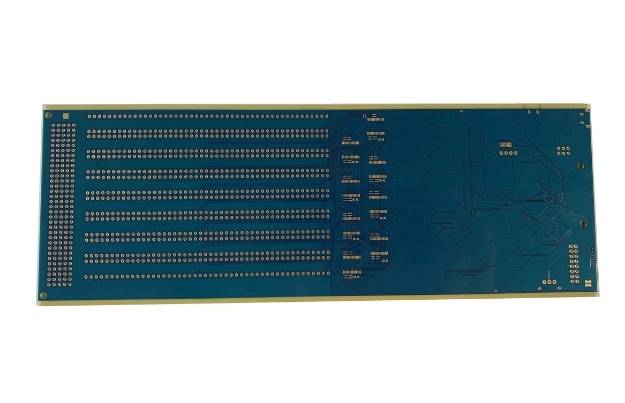
4 layer PCB means there are 4 layers to rout electrical signals: Top Layer, Inner Layer 1, Inner Layer 2, and Bottom Layer.
SMTFAB has one expert engineering and production team, they can provide professional advice for your 4 layer PCB project.
What’s more, SMTFAB can offer a turnkey solution for your project. From PCB design & layout, PCB fabrication to PCB assembly, all processes are in-house and not outsourcing.
If you are looking for a reputable 4 layer PCB supplier for your project and business, SMTFAB is your best choice.
In order to support you, our sales team is working to follow up on your local time. When you have an urgent project, we can help you to produce it with 48h quick-turn service.
There are many different applications for 4 layer PCB, such as power supply, medical device, automotive, industrial controls, smartphones, GPS systems, motion systems, and satellites.
SMTFAB has passed ISO 19001 and 14000 certifications, so we always offer top-quality to our customers.
SMTFAB has over 500 workers in our workshop and the monthly capacity is 40,000 square meters. We can meet your different demands from prototype to mass production.
When you have a new inquiry, we are always here to support you.
4 Layer PCB: The Ultimate FAQ Guide
Are you looking for a PCB FAQ guide with all the information about 4-layer PCB?
Then here is your chance to get a detailed look at all the relevant information on 4-layer PCB through this FAQ guide.
- What Is A 4 Layer PCB?
- How Is 4 Layer PCB Different Form Other Types Of PCBs?
- How Does A 4 Layer PCB Achieve Low Noise On The Power Cord?
- What Are The Different Copper Cylinders On 4 Layer PCBs Called?
- How Is The Routing Performed Of A 4 Layer PCB?
- What Are The Benefits Of A 4 Layer PCB?
- Does A 4 Layer PCB Have A SIGNAL Loop?
- What Is The Maximum Amount Of Current That A 4 Layer PCB Can Carry?
- What Type Of Circuit Board Does A 4 Layer PCB Have?
- What Are The Locations Of Power And Ground Plane In A 4 Layer PCB?
- Does Thickness Matter In A 4 Layer PCB?
- When Should I Choose A 4 Layer PCB Instead Of A Single Layer PCB?
- Is It Necessary For A 4 Layer PCB To Be Green?
- What Other Metals Apart From Copper Can Be Used In A 4 Layer PCB?
- What Is The Process Of Making Traces On A 4 Layer PCB?
- Do Manufacturers Use Fiberglass In The Manufacturing Of A 4 Layer PCB?
- What Us A Capacitance Test In Relation To A 4 Layer PCB?
- What Components Can Be Used On A 4 Layer PCB?
- What Are The Applications Of A 4 Layer PCB?
- What is the Manufacturing Process of a 4 Layer PCB?
- What is the Difference Between 4 Layers and 2 Layer PCB?
- What is the Difference Between 4 Layers and 6 Layer PCB?
What Is A 4 Layer PCB?
A 4 layer PCB is a circuit board that consists of 4 glass fiber layers or conductive copper traces that help to route the signals.
There are 4 layers, and each one of them is identified as a bottom layer, inner layer 1. Inner layer 2 and top layer.

4-Layer PCB
The inner layers are also called VCC and GND, which are connected through buried holes or blind holes.
The conductive material like copper in these PCB boards provides solder masks, and these copper strips are sealed in the board with 3 inner dielectrics divided internally.
These copper layers are in well-defined sequence, and they are called signal layers because they play a significant role in routing.
Each layer has its role and functionality to complete the connection for signals.
SMTFAB is now offering the best 4 layer PCB in China with the best services for your business.
How Is 4 Layer PCB Different Form Other Types Of PCBs?
A 4 layer PCB differentiates from other types of PCBs such as a 2-layer PCB because the design of a 4-layer PCB has its own complexity.
The difference can be seen in the thickness as well as in the time of development when a PCB is processed and manufactured.
The cost is additionally a great difference between these PCBs because a complex PCB board like 4-layer requires more quantity of material which raises the cost.
A 2-layer PCB is cheaper and less expensive because the complexity is not so much to be found, and it’s easier to design with less time required for manufacturing.
Each of these PCBs has their equivalent number of sided traces on them, such as a 2-layer PCB will have two-sided traces with its bottom and top layer where 4-layer PCB will have 4 layers.
1-layer or 2-layer is not good enough as 4-layer PCB as it’s always better to use four because of its support for high-level complexity having four copper layers on it.
How Does A 4 Layer PCB Achieve Low Noise On The Power Cord?
As a 4 layer, PCB has quadruple layers of copper on its board augmented together for routing the signals; these layers help to minimize the interference level as well.

4-Layer PCB Stack-up
The quality of such PCB is higher, which reaches reduced noise levels and allows to reduce the distortion as well, which helps to achieve low noise on the power cord.
The reduction of inductance in the power cable as well as in the ground causes a reduction of voltage noise pretty easily.
What Are The Different Copper Cylinders On 4 Layer PCBs Called?
There are copper cylinders on a 4 layer PCB because of its copper layers, and they are called VIAS.
The function of these vias is to transfer and conduct heat and electricity through the board within the limits of the structure provided by copper layers.
The buried vias are in the center of the internal and external layer that provides a connection between them.
For connecting the internal layers, blind vias play an important role, and such vias can not be identified through visual inspection because they are sealed during the soldering process.
It is important to carefully seal these vias as they can disable the functionality if things go wrong at any point.
These vias are used for the following reasons in a PCB.
- The wire management in a PCB board can be done effectively through vias.
- These vias have better management when we consider spacing.
- The density of a board’s components can be increased by using vias.
- These vias play a great role in manufacturing smaller PCB boards that can be used in technical devices or smaller portable instruments.
How Is The Routing Performed Of A 4 Layer PCB?
The routing in a 4-layer PCB is performed by developing some connections in each of the layers having its own specific role for the process that is being carried out.
In routing, the inner layers become the core of this 4-layer PCB, and the bottom and top layers are routed to give out complete connectivity for the components.

Performed Of A 4 Layer PCB
The inner layer 1 acts as a power plane in the circuit, whereas layer 2 helps the process as a ground plane.
The phenomenon is basically meant to be applied to reduce the noise and provide stable signal connectivity in the analog ground planes.
It is not possible to accurately implement this process which is why it is important to route all the traces that are moving towards a particular region to the other.
If these traces are not moved, they act as an antenna to transmit signals which is why a full single ground is preferred because it is reliable and gives better results for routing.
What Are The Benefits Of A 4 Layer PCB?
A 4-layer PCB has various benefits if you get it from the best manufacturers, such as PCB may who are the leading manufacturers in China.
- These PCBs help to improve EMI performance, and they can be used with portable devices if the PCB board is of a smaller size.
- They greatly help to miniaturize the design as well as deal with complex routing very easily.
- The layered design of these smaller size PCBs help to provide the same functionality at less cost and in small devices easily.
- They have less weight and multiple connectors, allowing them to transmit and receive various signals by interlinking with multiple devices.
- They are very beneficial for all the modern electronics as they provide better mobility and they are easier to fabricate as well.
- A 4-layer PCB has better weight capacity, and it can resist high temperatures that they have to face during lamination.
- The flexible properties of these PCB boards help them to have long-lasting life and better bending capability.
- Usually, these PCB boards have a higher capacity to handle power than a 2-layer PCB board which is why they are always a better option providing increased connectivity.
- The multiple layers of insulation on these boards provide them with better durability for all types of usage in any situation having protective materials on them.
- Their electrical properties can help them to adapt and achieve a higher electrical density with their multilayers and make them more connective.
- They are best to use with a single connection point as they provide a single connection to the final product that comes of great use for small and portable devices and electronics.
Does A 4 Layer PCB Have A SIGNAL Loop?
A 4-layer PCB has a signal loop area with four layers of copper.

4-Layer PCB Signal Loop
These layers form the power and ground planes with the inner layers of the PCB that become large distributed capacitor that allows good power supply frequency.
The signal loop area fluctuates after when you separate the power plane from the ground.
What Is The Maximum Amount Of Current That A 4 Layer PCB Can Carry?
Normally, the maximum current that a 4-layer PCB 50mil-trace can carry is 2.6 amps.
This amount can vary depending on the thickness of the trace used on the board.
A thicker copper trace, if used on a 4-layer PCB board, will allow more current to flow through it.
In case you have a 4-layer PCB with a wider trace, in that case, it will still have more current capacity on the board.
You can get the highest current carrying capacity of 4-layer PCB boards from SMTFAB who offers the best quality products in China.
What Type Of Circuit Board Does A 4 Layer PCB Have?
A 4-layer PCB has a multi-layer board for the circuit as it is meant to deal with high temperatures and more current flow for better performance.

Multilayer PCB
All of these layers in these boards act as power and ground planes to provide proper routing for the signals, and they are fashioned separately from one another.
This formation of layer plays a major role in providing a better-reduced voltage noise and great electromagnetic conduction.
The power cord noise is also reduced with such PCB boards, and it ensures that a reduced area of signal loops is formed for better transmission of signals.
Such configuration greatly helps to increased the functionality of the overall performance of the board.
What Are The Locations Of Power And Ground Plane In A 4 Layer PCB?
The power and ground planes are situated in the center of a 4-layer PCB forming a stable connection having with two inner layers.
These planes are useful to connect the PCB to a ground source, and a power source, and they are called inner layer 1 and inner layer 2.
The inner layers allow easy connection for the components with the ground and power sources through the planes, making a simple and stable connection.
These ground and solid power planes play a major role in deducting the electromagnetic interference caused by the phenomenon so that signal quality can be enhanced.
Does Thickness Matter In A 4 Layer PCB?
The thickness really matters in a 4-layer PCB because a thicker board has more current carrying capability and better resistance to heat temperatures.

4-Layer PCB Thickness
It is crucial for the design of a 4-layer PCB board, without which it won’t be considered a good board.
A less thick PCB is most likely to end up being compromised or result in a weak board with less performance that can break at any point.
Sometimes, a weak board can easily get short circuits and even lead to component failure in many situations.
The thickness matters a lot when you consider the use of a PCB board in any circuit or device.
PCB may offer the thickest and best quality 4-layer PCB boards with a warranty that is sold throughout China.
When Should I Choose A 4 Layer PCB Instead Of A Single Layer PCB?
A 4-layer PCB has various advantages over single-layer PCB, and you should consider the following reasons when choosing a 4-layer over a single-layer PCB.
- A 4-layer board is thicker and wide, which makes it ideal to use in a situation where your project is meant to be used for bigger purposes and heavy load.
- It has a more accommodating design which is why it has more functionality as compared to single-layer PCB.
- There are broader functions and current carrying capacity in a 4-layer PCB.
- A 4-layer PCB goes through complex production, which enables it to be more flexible and a diverse option as a suitable choice with various components.
- The cost of a 4-layer PCB may be higher as compared to a single-layer PCB, but it provides a better and stable connection.
- Board durability matters a lot as a 4-layer PCB board will have more durability and longer life than a single layer PCB which is why you should consider the optimal conditions.
Is It Necessary For A 4 Layer PCB To Be Green?
It is not quite necessary for a 4-layer PCB to be green because the color doesn’t matter.
The only thing that matters in PCB is the quality and performance that the board has to offer.

Green Soldermask
PCB boards come in different colors like green, black, blue, which is not important as it doesn’t affect the performance of aboard.
Mostly the PCB boards are found green because the solder mask that is applied to these boards is formed in green, but there are other options as well, such as white, yellow, and even red sometimes.
This solder mask gives color to the board, and it is basically meant to protect the copper traces over a board from oxidation.
What Other Metals Apart From Copper Can Be Used In A 4 Layer PCB?
Conductive metals like nickel, tin, aluminum, and gold can also be used in a 4-layer PCB instead of copper.
Copper is a commonly used material in the traces because it provides good conductivity of the current through the board having large charge flow capacity and availability with its cheap cost.
Nickel and tin are not as good as copper conductors, which is why copper has an advantage over them, and aluminum and gold are pretty expensive than copper, which again makes the copper ideal choice.
However, all of these metals are good conductors, and they can be used to manufacture 4-layer PCBs.
SMTFAB be offering 4-layer PCB boards with all types of metal construction according to the customer’s need.
What Is The Process Of Making Traces On A 4 Layer PCB?
There are two methods to make traces on a 4-layer PCB board, and both of them help to provide conductive traces that help in better transfer of electrical charges.

Traces On A 4 Layer PCB
Subtractive Method
- A copper film is etched in this method to produce a conductive trace for the PCB.
- The excess of copper is removed by using some chemical agents that only leaves conductive pattern behind.
- A protective material is applied to the traces so that no reaction occurs with the chemicals used.
Additive Method
- In this approach, the conductive metal is added with the plates that form a trace pattern that is required.
- It is formed through the insertion method, and plating can be used as well, along with paste screening.
- It helps to produce traces on a 4-layer PCB board having a desired weight for the conductive metal.
https://youtu.be/-33H33j67wA
Do Manufacturers Use Fiberglass In The Manufacturing Of A 4 Layer PCB?
Fiberglass is ideal to use in the manufacturing of a 4-layer PCB because it is a plastic compound having good properties when used with glass.
It is a cheap material that saves the cost of manufacturing PCB while providing good strength and weight to the board.
This flexible material is very much transparent to electromagnetic radiation, which helps to deform into any required shape easily.
It allows holding all the layers of 4-layer PCB in a firm point.
What Us A Capacitance Test In Relation To A 4 Layer PCB?
A capacitance test is a necessary and useful test that helps to find any openings and shorts on the circuit board of a 4-layer PCB.

Red Soldermask of 4-Layer PCB
This test allows leaving an electric charge on the board that allows the designers to check and identify the isolations and continuity with the use of probes.
What Components Can Be Used On A 4 Layer PCB?
A 4-layer PCB consists of several components as it is a pretty complex situation to develop such PCB boards.
- A capacitor is used that helps to store the electrical charge.
- Transistor on 4-layer PCB helps to distribute the electric charges into the diodes as well as the circuit.
- A voltage source and electronic capacitor regulars the charge.
- An electronic diode that allows the flow of charge in a specific direction and also protects the circuit from high voltage damages.
- Electronic transistors help to control electrical charges.
- IC chips for various functions such as the conversion of signals.
What Are The Applications Of A 4 Layer PCB?
There are various applications of 4-layer PCB, and they are listed below.
- The major use of such types of PCBs is found in electronic mainboards for servers because of their resistance to heat and temperatures.
- They are also used in automobiles in the formation of electrical systems and controls.
- They are used in GPS systems and satellite applications.
- They are used in the medical field, such as in machines like X-ray and heart monitor sensors.
- They are also used in smaller and portable electronic devices that you use on a daily basis in your house.
What is the Manufacturing Process of a 4 Layer PCB?
The manufacturing of the 4-layer PCB process includes these steps

The manufacturing of the 4-layer PCB
- A corrosion-resistant layer is applied for making a good etching pattern for which chemicals are applied to clean the layers.
- Then, a dry film is applied to the inner layers of the PCB that gives the desired shape by peeling off the polyethylene film and applying a copper surface with heat and pressure.
- Then, image exposure and development take place with the irradiation of UV light, and it is kept for some time. The image shouldn’t be removed for 15 minutes before developing.
- Then, the desired circuit pattern is formed with copper etching to deduct the useless portion of copper foil using chemicals.
- Then, the resistant layer is cleaned up, which leaves the copper foil exposed, and then waste materials are taken care of, and they are properly filtered.
- Washing is required after stripping resistance, and then the board is dried completely.
- Then, inner layers are prepared for the treatment of oxidation, and prepreg is impregnated with glass fiber.
- A multi-layer lamination is applied with pressure on the board while covering existing inner players from both sides with copper foil. Then the board is cooled down.
- Then 100microns holes are drilled in diameter with the help of a computer-driven machine for managing the movement of the drill.
- Then, the copper lining on the edge is scraped off properly, and then a thin copper layer is applied to the hole with a chemical deposition process.
- The outer layers of the PCB are coated after removing the photoresist to make the copper layers thick.
- Then etching is done, and a solder mask is applied with a clear finishing for a better look.
- At last, embossing the PCB board is done with ink-jet writing for marking the board with vital information.
- The last PCB test is performed for the electrical conduction of the board to ensure its functionality.
What is the Difference Between 4 Layers and 2 Layer PCB?
A 4-layer PCB has four layers of copper traces, whereas two layers PCB has only two-sided traces.

4-Layer PCB
A 4-layer is better in performance and thermal conductivity along with the current flow in the circuit.
What is the Difference Between 4 Layers and 6 Layer PCB?
A 6-layer PCB has more space for wiring that allows more connectivity and a stronger board.

6-Layer PCB
A PCB having more wires is a 6-layer PCB with good performance, whereas a PCB with four layers trace is a 4-layer PCB that is also having a better performance for portable devices.
Your Outstanding 4 Layer PCB Manufacturer in China
As one professional 4 layer PCB supplier in China, we can provide a one-stop solution for your project.
- Over 12 years 4 layer PCB manufacturing experience
- Sufficient raw materials in stock
- 100% E-test and AOI inspection
- Certified with the USA and Canada UL
- 48h quick-turn service for your prototype 4 layer PCB
- 7/24 sales and engineering tech support
- Production Facility
- PCB Capabilities
- 4 layer PCB Stackup
| Feature | Capability |
| Quality Grade | Standard IPC 2 and IPC 3 |
| Number of Layers | 2 – 40layers |
| Order Quantity | 1pc – 1Million+pcs |
| Build Time | 24H – 4weeks |
| Material | S1150G, S1165, S1000-2 |
| Board Size | Min 5*5mm | Max 500*650mm |
| Board Thickness | 0.4mm – 6.5mm |
| Copper Weight (Finished) | 0.5oz – 10.0oz |
| Min Tracing/Spacing | 3mil/3mil |
| Solder Mask Sides | As per the file |
| Solder Mask Color | Green, White, Blue, Black, Red, Yellow |
| Silkscreen Sides | As per the file |
| Silkscreen Color | White, Black, Yellow |
| Surface Finish | HASL – Hot Air Solder Leveling |
| Lead-Free HASL – RoHS | |
| ENIG – Electroless Nickle/Immersion Gold – RoHS | |
| Immersion Silver – RoHS | |
| Immersion Tin – RoHS | |
| OSP – Organic Solderability Preservatives – RoHS | |
| Min Annular Ring | 4mil |
| Min Drilling Hole Diameter | 6mil |
| Other Techniques | Gold fingers |
| Blind/Buried Vias |
Please see the details of 4 layer PCB Stack-up as follows:
Releted Some Other PCBs
Why Choose SMTFAB for Your 4 Layer PCB
SMTFAB is one leading 4 layer PCB manufacturer for over 12 years in China. Throughout the years of offering high-quality and perfect service, SMTFAB has become the most reliable 4 layer PCB supplier in China.
4 layer PCB means there are 4 layers to rout electrical signals: Top Layer, Inner Layer 1, Inner Layer 2, and Bottom Layer.
SMTFAB has one expert engineering and production team, they can provide professional advice for your 4 layer PCB project.
What’s more, SMTFAB can offer a turnkey solution for your project. From PCB design & layout, PCB fabrication to PCB assembly, all processes are in-house and not outsourcing.
If you are looking for a reputable 4 layer PCB supplier for your project and business, SMTFAB is your best choice.
In order to support you, our sales team is working to follow up on your local time. When you have an urgent project, we can help you to produce it with 48h quick-turn service.
There are many different applications for 4 layer PCB, such as power supply, medical device, automotive, industrial controls, smartphones, GPS systems, motion systems, and satellites.
SMTFAB has passed ISO 19001 and 14000 certifications, so we always offer top-quality to our customers.
SMTFAB has over 500 workers in our workshop and the monthly capacity is 40,000 square meters. We can meet your different demands from prototype to mass production.
When you have a new inquiry, we are always here to support you.
4 Layer PCB: The Ultimate FAQ Guide
Are you looking for a PCB FAQ guide with all the information about 4-layer PCB?
Then here is your chance to get a detailed look at all the relevant information on 4-layer PCB through this FAQ guide.
- What Is A 4 Layer PCB?
- How Is 4 Layer PCB Different Form Other Types Of PCBs?
- How Does A 4 Layer PCB Achieve Low Noise On The Power Cord?
- What Are The Different Copper Cylinders On 4 Layer PCBs Called?
- How Is The Routing Performed Of A 4 Layer PCB?
- What Are The Benefits Of A 4 Layer PCB?
- Does A 4 Layer PCB Have A SIGNAL Loop?
- What Is The Maximum Amount Of Current That A 4 Layer PCB Can Carry?
- What Type Of Circuit Board Does A 4 Layer PCB Have?
- What Are The Locations Of Power And Ground Plane In A 4 Layer PCB?
- Does Thickness Matter In A 4 Layer PCB?
- When Should I Choose A 4 Layer PCB Instead Of A Single Layer PCB?
- Is It Necessary For A 4 Layer PCB To Be Green?
- What Other Metals Apart From Copper Can Be Used In A 4 Layer PCB?
- What Is The Process Of Making Traces On A 4 Layer PCB?
- Do Manufacturers Use Fiberglass In The Manufacturing Of A 4 Layer PCB?
- What Us A Capacitance Test In Relation To A 4 Layer PCB?
- What Components Can Be Used On A 4 Layer PCB?
- What Are The Applications Of A 4 Layer PCB?
- What is the Manufacturing Process of a 4 Layer PCB?
- What is the Difference Between 4 Layers and 2 Layer PCB?
- What is the Difference Between 4 Layers and 6 Layer PCB?
What Is A 4 Layer PCB?
A 4 layer PCB is a circuit board that consists of 4 glass fiber layers or conductive copper traces that help to route the signals.
There are 4 layers, and each one of them is identified as a bottom layer, inner layer 1. Inner layer 2 and top layer.
4-Layer PCB
The inner layers are also called VCC and GND, which are connected through buried holes or blind holes.
The conductive material like copper in these PCB boards provides solder masks, and these copper strips are sealed in the board with 3 inner dielectrics divided internally.
These copper layers are in well-defined sequence, and they are called signal layers because they play a significant role in routing.
Each layer has its role and functionality to complete the connection for signals.
SMTFAB is now offering the best 4 layer PCB in China with the best services for your business.
How Is 4 Layer PCB Different Form Other Types Of PCBs?
A 4 layer PCB differentiates from other types of PCBs such as a 2-layer PCB because the design of a 4-layer PCB has its own complexity.
The difference can be seen in the thickness as well as in the time of development when a PCB is processed and manufactured.
The cost is additionally a great difference between these PCBs because a complex PCB board like 4-layer requires more quantity of material which raises the cost.
A 2-layer PCB is cheaper and less expensive because the complexity is not so much to be found, and it’s easier to design with less time required for manufacturing.
Each of these PCBs has their equivalent number of sided traces on them, such as a 2-layer PCB will have two-sided traces with its bottom and top layer where 4-layer PCB will have 4 layers.
1-layer or 2-layer is not good enough as 4-layer PCB as it’s always better to use four because of its support for high-level complexity having four copper layers on it.
How Does A 4 Layer PCB Achieve Low Noise On The Power Cord?
As a 4 layer, PCB has quadruple layers of copper on its board augmented together for routing the signals; these layers help to minimize the interference level as well.
4-Layer PCB Stack-up
The quality of such PCB is higher, which reaches reduced noise levels and allows to reduce the distortion as well, which helps to achieve low noise on the power cord.
The reduction of inductance in the power cable as well as in the ground causes a reduction of voltage noise pretty easily.
What Are The Different Copper Cylinders On 4 Layer PCBs Called?
There are copper cylinders on a 4 layer PCB because of its copper layers, and they are called VIAS.
The function of these vias is to transfer and conduct heat and electricity through the board within the limits of the structure provided by copper layers.
The buried vias are in the center of the internal and external layer that provides a connection between them.
For connecting the internal layers, blind vias play an important role, and such vias can not be identified through visual inspection because they are sealed during the soldering process.
It is important to carefully seal these vias as they can disable the functionality if things go wrong at any point.
These vias are used for the following reasons in a PCB.
- The wire management in a PCB board can be done effectively through vias.
- These vias have better management when we consider spacing.
- The density of a board’s components can be increased by using vias.
- These vias play a great role in manufacturing smaller PCB boards that can be used in technical devices or smaller portable instruments.
How Is The Routing Performed Of A 4 Layer PCB?
The routing in a 4-layer PCB is performed by developing some connections in each of the layers having its own specific role for the process that is being carried out.
In routing, the inner layers become the core of this 4-layer PCB, and the bottom and top layers are routed to give out complete connectivity for the components.
Performed Of A 4 Layer PCB
The inner layer 1 acts as a power plane in the circuit, whereas layer 2 helps the process as a ground plane.
The phenomenon is basically meant to be applied to reduce the noise and provide stable signal connectivity in the analog ground planes.
It is not possible to accurately implement this process which is why it is important to route all the traces that are moving towards a particular region to the other.
If these traces are not moved, they act as an antenna to transmit signals which is why a full single ground is preferred because it is reliable and gives better results for routing.
What Are The Benefits Of A 4 Layer PCB?
A 4-layer PCB has various benefits if you get it from the best manufacturers, such as PCB may who are the leading manufacturers in China.
- These PCBs help to improve EMI performance, and they can be used with portable devices if the PCB board is of a smaller size.
- They greatly help to miniaturize the design as well as deal with complex routing very easily.
- The layered design of these smaller size PCBs help to provide the same functionality at less cost and in small devices easily.
- They have less weight and multiple connectors, allowing them to transmit and receive various signals by interlinking with multiple devices.
- They are very beneficial for all the modern electronics as they provide better mobility and they are easier to fabricate as well.
- A 4-layer PCB has better weight capacity, and it can resist high temperatures that they have to face during lamination.
- The flexible properties of these PCB boards help them to have long-lasting life and better bending capability.
- Usually, these PCB boards have a higher capacity to handle power than a 2-layer PCB board which is why they are always a better option providing increased connectivity.
- The multiple layers of insulation on these boards provide them with better durability for all types of usage in any situation having protective materials on them.
- Their electrical properties can help them to adapt and achieve a higher electrical density with their multilayers and make them more connective.
- They are best to use with a single connection point as they provide a single connection to the final product that comes of great use for small and portable devices and electronics.
Does A 4 Layer PCB Have A SIGNAL Loop?
A 4-layer PCB has a signal loop area with four layers of copper.
4-Layer PCB Signal Loop
These layers form the power and ground planes with the inner layers of the PCB that become large distributed capacitor that allows good power supply frequency.
The signal loop area fluctuates after when you separate the power plane from the ground.
What Is The Maximum Amount Of Current That A 4 Layer PCB Can Carry?
Normally, the maximum current that a 4-layer PCB 50mil-trace can carry is 2.6 amps.
This amount can vary depending on the thickness of the trace used on the board.
A thicker copper trace, if used on a 4-layer PCB board, will allow more current to flow through it.
In case you have a 4-layer PCB with a wider trace, in that case, it will still have more current capacity on the board.
You can get the highest current carrying capacity of 4-layer PCB boards from SMTFAB who offers the best quality products in China.
What Type Of Circuit Board Does A 4 Layer PCB Have?
A 4-layer PCB has a multi-layer board for the circuit as it is meant to deal with high temperatures and more current flow for better performance.
Multilayer PCB
All of these layers in these boards act as power and ground planes to provide proper routing for the signals, and they are fashioned separately from one another.
This formation of layer plays a major role in providing a better-reduced voltage noise and great electromagnetic conduction.
The power cord noise is also reduced with such PCB boards, and it ensures that a reduced area of signal loops is formed for better transmission of signals.
Such configuration greatly helps to increased the functionality of the overall performance of the board.
What Are The Locations Of Power And Ground Plane In A 4 Layer PCB?
The power and ground planes are situated in the center of a 4-layer PCB forming a stable connection having with two inner layers.
These planes are useful to connect the PCB to a ground source, and a power source, and they are called inner layer 1 and inner layer 2.
The inner layers allow easy connection for the components with the ground and power sources through the planes, making a simple and stable connection.
These ground and solid power planes play a major role in deducting the electromagnetic interference caused by the phenomenon so that signal quality can be enhanced.
Does Thickness Matter In A 4 Layer PCB?
The thickness really matters in a 4-layer PCB because a thicker board has more current carrying capability and better resistance to heat temperatures.
4-Layer PCB Thickness
It is crucial for the design of a 4-layer PCB board, without which it won’t be considered a good board.
A less thick PCB is most likely to end up being compromised or result in a weak board with less performance that can break at any point.
Sometimes, a weak board can easily get short circuits and even lead to component failure in many situations.
The thickness matters a lot when you consider the use of a PCB board in any circuit or device.
PCB may offer the thickest and best quality 4-layer PCB boards with a warranty that is sold throughout China.
When Should I Choose A 4 Layer PCB Instead Of A Single Layer PCB?
A 4-layer PCB has various advantages over single-layer PCB, and you should consider the following reasons when choosing a 4-layer over a single-layer PCB.
- A 4-layer board is thicker and wide, which makes it ideal to use in a situation where your project is meant to be used for bigger purposes and heavy load.
- It has a more accommodating design which is why it has more functionality as compared to single-layer PCB.
- There are broader functions and current carrying capacity in a 4-layer PCB.
- A 4-layer PCB goes through complex production, which enables it to be more flexible and a diverse option as a suitable choice with various components.
- The cost of a 4-layer PCB may be higher as compared to a single-layer PCB, but it provides a better and stable connection.
- Board durability matters a lot as a 4-layer PCB board will have more durability and longer life than a single layer PCB which is why you should consider the optimal conditions.
Is It Necessary For A 4 Layer PCB To Be Green?
It is not quite necessary for a 4-layer PCB to be green because the color doesn’t matter.
The only thing that matters in PCB is the quality and performance that the board has to offer.
Green Soldermask
PCB boards come in different colors like green, black, blue, which is not important as it doesn’t affect the performance of aboard.
Mostly the PCB boards are found green because the solder mask that is applied to these boards is formed in green, but there are other options as well, such as white, yellow, and even red sometimes.
This solder mask gives color to the board, and it is basically meant to protect the copper traces over a board from oxidation.
What Other Metals Apart From Copper Can Be Used In A 4 Layer PCB?
Conductive metals like nickel, tin, aluminum, and gold can also be used in a 4-layer PCB instead of copper.
Copper is a commonly used material in the traces because it provides good conductivity of the current through the board having large charge flow capacity and availability with its cheap cost.
Nickel and tin are not as good as copper conductors, which is why copper has an advantage over them, and aluminum and gold are pretty expensive than copper, which again makes the copper ideal choice.
However, all of these metals are good conductors, and they can be used to manufacture 4-layer PCBs.
SMTFAB be offering 4-layer PCB boards with all types of metal construction according to the customer’s need.
What Is The Process Of Making Traces On A 4 Layer PCB?
There are two methods to make traces on a 4-layer PCB board, and both of them help to provide conductive traces that help in better transfer of electrical charges.
Traces On A 4 Layer PCB
Subtractive Method
- A copper film is etched in this method to produce a conductive trace for the PCB.
- The excess of copper is removed by using some chemical agents that only leaves conductive pattern behind.
- A protective material is applied to the traces so that no reaction occurs with the chemicals used.
Additive Method
- In this approach, the conductive metal is added with the plates that form a trace pattern that is required.
- It is formed through the insertion method, and plating can be used as well, along with paste screening.
- It helps to produce traces on a 4-layer PCB board having a desired weight for the conductive metal.
https://youtu.be/-33H33j67wA
Do Manufacturers Use Fiberglass In The Manufacturing Of A 4 Layer PCB?
Fiberglass is ideal to use in the manufacturing of a 4-layer PCB because it is a plastic compound having good properties when used with glass.
It is a cheap material that saves the cost of manufacturing PCB while providing good strength and weight to the board.
This flexible material is very much transparent to electromagnetic radiation, which helps to deform into any required shape easily.
It allows holding all the layers of 4-layer PCB in a firm point.
What Us A Capacitance Test In Relation To A 4 Layer PCB?
A capacitance test is a necessary and useful test that helps to find any openings and shorts on the circuit board of a 4-layer PCB.
Red Soldermask of 4-Layer PCB
This test allows leaving an electric charge on the board that allows the designers to check and identify the isolations and continuity with the use of probes.
What Components Can Be Used On A 4 Layer PCB?
A 4-layer PCB consists of several components as it is a pretty complex situation to develop such PCB boards.
- A capacitor is used that helps to store the electrical charge.
- Transistor on 4-layer PCB helps to distribute the electric charges into the diodes as well as the circuit.
- A voltage source and electronic capacitor regulars the charge.
- An electronic diode that allows the flow of charge in a specific direction and also protects the circuit from high voltage damages.
- Electronic transistors help to control electrical charges.
- IC chips for various functions such as the conversion of signals.
What Are The Applications Of A 4 Layer PCB?
There are various applications of 4-layer PCB, and they are listed below.
- The major use of such types of PCBs is found in electronic mainboards for servers because of their resistance to heat and temperatures.
- They are also used in automobiles in the formation of electrical systems and controls.
- They are used in GPS systems and satellite applications.
- They are used in the medical field, such as in machines like X-ray and heart monitor sensors.
- They are also used in smaller and portable electronic devices that you use on a daily basis in your house.
What is the Manufacturing Process of a 4 Layer PCB?
The manufacturing of the 4-layer PCB process includes these steps
The manufacturing of the 4-layer PCB
- A corrosion-resistant layer is applied for making a good etching pattern for which chemicals are applied to clean the layers.
- Then, a dry film is applied to the inner layers of the PCB that gives the desired shape by peeling off the polyethylene film and applying a copper surface with heat and pressure.
- Then, image exposure and development take place with the irradiation of UV light, and it is kept for some time. The image shouldn’t be removed for 15 minutes before developing.
- Then, the desired circuit pattern is formed with copper etching to deduct the useless portion of copper foil using chemicals.
- Then, the resistant layer is cleaned up, which leaves the copper foil exposed, and then waste materials are taken care of, and they are properly filtered.
- Washing is required after stripping resistance, and then the board is dried completely.
- Then, inner layers are prepared for the treatment of oxidation, and prepreg is impregnated with glass fiber.
- A multi-layer lamination is applied with pressure on the board while covering existing inner players from both sides with copper foil. Then the board is cooled down.
- Then 100microns holes are drilled in diameter with the help of a computer-driven machine for managing the movement of the drill.
- Then, the copper lining on the edge is scraped off properly, and then a thin copper layer is applied to the hole with a chemical deposition process.
- The outer layers of the PCB are coated after removing the photoresist to make the copper layers thick.
- Then etching is done, and a solder mask is applied with a clear finishing for a better look.
- At last, embossing the PCB board is done with ink-jet writing for marking the board with vital information.
- The last PCB test is performed for the electrical conduction of the board to ensure its functionality.
What is the Difference Between 4 Layers and 2 Layer PCB?
A 4-layer PCB has four layers of copper traces, whereas two layers PCB has only two-sided traces.
4-Layer PCB
A 4-layer is better in performance and thermal conductivity along with the current flow in the circuit.
What is the Difference Between 4 Layers and 6 Layer PCB?
A 6-layer PCB has more space for wiring that allows more connectivity and a stronger board.
6-Layer PCB
A PCB having more wires is a 6-layer PCB with good performance, whereas a PCB with four layers trace is a 4-layer PCB that is also having a better performance for portable devices.
Your Outstanding 4 Layer PCB Manufacturer in China
As one professional 4 layer PCB supplier in China, we can provide a one-stop solution for your project.
- Over 12 years 4 layer PCB manufacturing experience
- Sufficient raw materials in stock
- 100% E-test and AOI inspection
- Certified with the USA and Canada UL
- 48h quick-turn service for your prototype 4 layer PCB
- 7/24 sales and engineering tech support
Your Outstanding 4 Layer PCB Manufacturer in China
Your Outstanding 4 Layer PCB Manufacturer in China
As one professional 4 layer PCB supplier in China, we can provide a one-stop solution for your project.
- Over 12 years 4 layer PCB manufacturing experience
- Sufficient raw materials in stock
- 100% E-test and AOI inspection
- Certified with the USA and Canada UL
- 48h quick-turn service for your prototype 4 layer PCB
- 7/24 sales and engineering tech support
- Production Facility
- PCB Capabilities
- 4 layer PCB Stackup
| Feature | Capability |
| Quality Grade | Standard IPC 2 and IPC 3 |
| Number of Layers | 2 – 40layers |
| Order Quantity | 1pc – 1Million+pcs |
| Build Time | 24H – 4weeks |
| Material | S1150G, S1165, S1000-2 |
| Board Size | Min 5*5mm | Max 500*650mm |
| Board Thickness | 0.4mm – 6.5mm |
| Copper Weight (Finished) | 0.5oz – 10.0oz |
| Min Tracing/Spacing | 3mil/3mil |
| Solder Mask Sides | As per the file |
| Solder Mask Color | Green, White, Blue, Black, Red, Yellow |
| Silkscreen Sides | As per the file |
| Silkscreen Color | White, Black, Yellow |
| Surface Finish | HASL – Hot Air Solder Leveling |
| Lead-Free HASL – RoHS | |
| ENIG – Electroless Nickle/Immersion Gold – RoHS | |
| Immersion Silver – RoHS | |
| Immersion Tin – RoHS | |
| OSP – Organic Solderability Preservatives – RoHS | |
| Min Annular Ring | 4mil |
| Min Drilling Hole Diameter | 6mil |
| Other Techniques | Gold fingers |
| Blind/Buried Vias |
Please see the details of 4 layer PCB Stack-up as follows:
- Production Facility
- PCB Capabilities
- 4 layer PCB Stackup
| Feature | Capability |
| Quality Grade | Standard IPC 2 and IPC 3 |
| Number of Layers | 2 – 40layers |
| Order Quantity | 1pc – 1Million+pcs |
| Build Time | 24H – 4weeks |
| Material | S1150G, S1165, S1000-2 |
| Board Size | Min 5*5mm | Max 500*650mm |
| Board Thickness | 0.4mm – 6.5mm |
| Copper Weight (Finished) | 0.5oz – 10.0oz |
| Min Tracing/Spacing | 3mil/3mil |
| Solder Mask Sides | As per the file |
| Solder Mask Color | Green, White, Blue, Black, Red, Yellow |
| Silkscreen Sides | As per the file |
| Silkscreen Color | White, Black, Yellow |
| Surface Finish | HASL – Hot Air Solder Leveling |
| Lead-Free HASL – RoHS | |
| ENIG – Electroless Nickle/Immersion Gold – RoHS | |
| Immersion Silver – RoHS | |
| Immersion Tin – RoHS | |
| OSP – Organic Solderability Preservatives – RoHS | |
| Min Annular Ring | 4mil |
| Min Drilling Hole Diameter | 6mil |
| Other Techniques | Gold fingers |
| Blind/Buried Vias |
Please see the details of 4 layer PCB Stack-up as follows:
Please see the details of 4 layer PCB Stack-up as follows:
Releted Some Other PCBs
Releted Some Other PCBs
Why Choose SMTFAB for Your 4 Layer PCB
SMTFAB is one leading 4 layer PCB manufacturer for over 12 years in China. Throughout the years of offering high-quality and perfect service, SMTFAB has become the most reliable 4 layer PCB supplier in China.
4 layer PCB means there are 4 layers to rout electrical signals: Top Layer, Inner Layer 1, Inner Layer 2, and Bottom Layer.
SMTFAB has one expert engineering and production team, they can provide professional advice for your 4 layer PCB project.
What’s more, SMTFAB can offer a turnkey solution for your project. From PCB design & layout, PCB fabrication to PCB assembly, all processes are in-house and not outsourcing.
If you are looking for a reputable 4 layer PCB supplier for your project and business, SMTFAB is your best choice.
In order to support you, our sales team is working to follow up on your local time. When you have an urgent project, we can help you to produce it with 48h quick-turn service.
There are many different applications for 4 layer PCB, such as power supply, medical device, automotive, industrial controls, smartphones, GPS systems, motion systems, and satellites.
SMTFAB has passed ISO 19001 and 14000 certifications, so we always offer top-quality to our customers.
SMTFAB has over 500 workers in our workshop and the monthly capacity is 40,000 square meters. We can meet your different demands from prototype to mass production.
When you have a new inquiry, we are always here to support you.
4 Layer PCB: The Ultimate FAQ Guide
Are you looking for a PCB FAQ guide with all the information about 4-layer PCB?
Then here is your chance to get a detailed look at all the relevant information on 4-layer PCB through this FAQ guide.
- What Is A 4 Layer PCB?
- How Is 4 Layer PCB Different Form Other Types Of PCBs?
- How Does A 4 Layer PCB Achieve Low Noise On The Power Cord?
- What Are The Different Copper Cylinders On 4 Layer PCBs Called?
- How Is The Routing Performed Of A 4 Layer PCB?
- What Are The Benefits Of A 4 Layer PCB?
- Does A 4 Layer PCB Have A SIGNAL Loop?
- What Is The Maximum Amount Of Current That A 4 Layer PCB Can Carry?
- What Type Of Circuit Board Does A 4 Layer PCB Have?
- What Are The Locations Of Power And Ground Plane In A 4 Layer PCB?
- Does Thickness Matter In A 4 Layer PCB?
- When Should I Choose A 4 Layer PCB Instead Of A Single Layer PCB?
- Is It Necessary For A 4 Layer PCB To Be Green?
- What Other Metals Apart From Copper Can Be Used In A 4 Layer PCB?
- What Is The Process Of Making Traces On A 4 Layer PCB?
- Do Manufacturers Use Fiberglass In The Manufacturing Of A 4 Layer PCB?
- What Us A Capacitance Test In Relation To A 4 Layer PCB?
- What Components Can Be Used On A 4 Layer PCB?
- What Are The Applications Of A 4 Layer PCB?
- What is the Manufacturing Process of a 4 Layer PCB?
- What is the Difference Between 4 Layers and 2 Layer PCB?
- What is the Difference Between 4 Layers and 6 Layer PCB?
What Is A 4 Layer PCB?
A 4 layer PCB is a circuit board that consists of 4 glass fiber layers or conductive copper traces that help to route the signals.
There are 4 layers, and each one of them is identified as a bottom layer, inner layer 1. Inner layer 2 and top layer.
4-Layer PCB
The inner layers are also called VCC and GND, which are connected through buried holes or blind holes.
The conductive material like copper in these PCB boards provides solder masks, and these copper strips are sealed in the board with 3 inner dielectrics divided internally.
These copper layers are in well-defined sequence, and they are called signal layers because they play a significant role in routing.
Each layer has its role and functionality to complete the connection for signals.
SMTFAB is now offering the best 4 layer PCB in China with the best services for your business.
How Is 4 Layer PCB Different Form Other Types Of PCBs?
A 4 layer PCB differentiates from other types of PCBs such as a 2-layer PCB because the design of a 4-layer PCB has its own complexity.
The difference can be seen in the thickness as well as in the time of development when a PCB is processed and manufactured.
The cost is additionally a great difference between these PCBs because a complex PCB board like 4-layer requires more quantity of material which raises the cost.
A 2-layer PCB is cheaper and less expensive because the complexity is not so much to be found, and it’s easier to design with less time required for manufacturing.
Each of these PCBs has their equivalent number of sided traces on them, such as a 2-layer PCB will have two-sided traces with its bottom and top layer where 4-layer PCB will have 4 layers.
1-layer or 2-layer is not good enough as 4-layer PCB as it’s always better to use four because of its support for high-level complexity having four copper layers on it.
How Does A 4 Layer PCB Achieve Low Noise On The Power Cord?
As a 4 layer, PCB has quadruple layers of copper on its board augmented together for routing the signals; these layers help to minimize the interference level as well.
4-Layer PCB Stack-up
The quality of such PCB is higher, which reaches reduced noise levels and allows to reduce the distortion as well, which helps to achieve low noise on the power cord.
The reduction of inductance in the power cable as well as in the ground causes a reduction of voltage noise pretty easily.
What Are The Different Copper Cylinders On 4 Layer PCBs Called?
There are copper cylinders on a 4 layer PCB because of its copper layers, and they are called VIAS.
The function of these vias is to transfer and conduct heat and electricity through the board within the limits of the structure provided by copper layers.
The buried vias are in the center of the internal and external layer that provides a connection between them.
For connecting the internal layers, blind vias play an important role, and such vias can not be identified through visual inspection because they are sealed during the soldering process.
It is important to carefully seal these vias as they can disable the functionality if things go wrong at any point.
These vias are used for the following reasons in a PCB.
- The wire management in a PCB board can be done effectively through vias.
- These vias have better management when we consider spacing.
- The density of a board’s components can be increased by using vias.
- These vias play a great role in manufacturing smaller PCB boards that can be used in technical devices or smaller portable instruments.
How Is The Routing Performed Of A 4 Layer PCB?
The routing in a 4-layer PCB is performed by developing some connections in each of the layers having its own specific role for the process that is being carried out.
In routing, the inner layers become the core of this 4-layer PCB, and the bottom and top layers are routed to give out complete connectivity for the components.
Performed Of A 4 Layer PCB
The inner layer 1 acts as a power plane in the circuit, whereas layer 2 helps the process as a ground plane.
The phenomenon is basically meant to be applied to reduce the noise and provide stable signal connectivity in the analog ground planes.
It is not possible to accurately implement this process which is why it is important to route all the traces that are moving towards a particular region to the other.
If these traces are not moved, they act as an antenna to transmit signals which is why a full single ground is preferred because it is reliable and gives better results for routing.
What Are The Benefits Of A 4 Layer PCB?
A 4-layer PCB has various benefits if you get it from the best manufacturers, such as PCB may who are the leading manufacturers in China.
- These PCBs help to improve EMI performance, and they can be used with portable devices if the PCB board is of a smaller size.
- They greatly help to miniaturize the design as well as deal with complex routing very easily.
- The layered design of these smaller size PCBs help to provide the same functionality at less cost and in small devices easily.
- They have less weight and multiple connectors, allowing them to transmit and receive various signals by interlinking with multiple devices.
- They are very beneficial for all the modern electronics as they provide better mobility and they are easier to fabricate as well.
- A 4-layer PCB has better weight capacity, and it can resist high temperatures that they have to face during lamination.
- The flexible properties of these PCB boards help them to have long-lasting life and better bending capability.
- Usually, these PCB boards have a higher capacity to handle power than a 2-layer PCB board which is why they are always a better option providing increased connectivity.
- The multiple layers of insulation on these boards provide them with better durability for all types of usage in any situation having protective materials on them.
- Their electrical properties can help them to adapt and achieve a higher electrical density with their multilayers and make them more connective.
- They are best to use with a single connection point as they provide a single connection to the final product that comes of great use for small and portable devices and electronics.
Does A 4 Layer PCB Have A SIGNAL Loop?
A 4-layer PCB has a signal loop area with four layers of copper.
4-Layer PCB Signal Loop
These layers form the power and ground planes with the inner layers of the PCB that become large distributed capacitor that allows good power supply frequency.
The signal loop area fluctuates after when you separate the power plane from the ground.
What Is The Maximum Amount Of Current That A 4 Layer PCB Can Carry?
Normally, the maximum current that a 4-layer PCB 50mil-trace can carry is 2.6 amps.
This amount can vary depending on the thickness of the trace used on the board.
A thicker copper trace, if used on a 4-layer PCB board, will allow more current to flow through it.
In case you have a 4-layer PCB with a wider trace, in that case, it will still have more current capacity on the board.
You can get the highest current carrying capacity of 4-layer PCB boards from SMTFAB who offers the best quality products in China.
What Type Of Circuit Board Does A 4 Layer PCB Have?
A 4-layer PCB has a multi-layer board for the circuit as it is meant to deal with high temperatures and more current flow for better performance.
Multilayer PCB
All of these layers in these boards act as power and ground planes to provide proper routing for the signals, and they are fashioned separately from one another.
This formation of layer plays a major role in providing a better-reduced voltage noise and great electromagnetic conduction.
The power cord noise is also reduced with such PCB boards, and it ensures that a reduced area of signal loops is formed for better transmission of signals.
Such configuration greatly helps to increased the functionality of the overall performance of the board.
What Are The Locations Of Power And Ground Plane In A 4 Layer PCB?
The power and ground planes are situated in the center of a 4-layer PCB forming a stable connection having with two inner layers.
These planes are useful to connect the PCB to a ground source, and a power source, and they are called inner layer 1 and inner layer 2.
The inner layers allow easy connection for the components with the ground and power sources through the planes, making a simple and stable connection.
These ground and solid power planes play a major role in deducting the electromagnetic interference caused by the phenomenon so that signal quality can be enhanced.
Does Thickness Matter In A 4 Layer PCB?
The thickness really matters in a 4-layer PCB because a thicker board has more current carrying capability and better resistance to heat temperatures.
4-Layer PCB Thickness
It is crucial for the design of a 4-layer PCB board, without which it won’t be considered a good board.
A less thick PCB is most likely to end up being compromised or result in a weak board with less performance that can break at any point.
Sometimes, a weak board can easily get short circuits and even lead to component failure in many situations.
The thickness matters a lot when you consider the use of a PCB board in any circuit or device.
PCB may offer the thickest and best quality 4-layer PCB boards with a warranty that is sold throughout China.
When Should I Choose A 4 Layer PCB Instead Of A Single Layer PCB?
A 4-layer PCB has various advantages over single-layer PCB, and you should consider the following reasons when choosing a 4-layer over a single-layer PCB.
- A 4-layer board is thicker and wide, which makes it ideal to use in a situation where your project is meant to be used for bigger purposes and heavy load.
- It has a more accommodating design which is why it has more functionality as compared to single-layer PCB.
- There are broader functions and current carrying capacity in a 4-layer PCB.
- A 4-layer PCB goes through complex production, which enables it to be more flexible and a diverse option as a suitable choice with various components.
- The cost of a 4-layer PCB may be higher as compared to a single-layer PCB, but it provides a better and stable connection.
- Board durability matters a lot as a 4-layer PCB board will have more durability and longer life than a single layer PCB which is why you should consider the optimal conditions.
Is It Necessary For A 4 Layer PCB To Be Green?
It is not quite necessary for a 4-layer PCB to be green because the color doesn’t matter.
The only thing that matters in PCB is the quality and performance that the board has to offer.
Green Soldermask
PCB boards come in different colors like green, black, blue, which is not important as it doesn’t affect the performance of aboard.
Mostly the PCB boards are found green because the solder mask that is applied to these boards is formed in green, but there are other options as well, such as white, yellow, and even red sometimes.
This solder mask gives color to the board, and it is basically meant to protect the copper traces over a board from oxidation.
What Other Metals Apart From Copper Can Be Used In A 4 Layer PCB?
Conductive metals like nickel, tin, aluminum, and gold can also be used in a 4-layer PCB instead of copper.
Copper is a commonly used material in the traces because it provides good conductivity of the current through the board having large charge flow capacity and availability with its cheap cost.
Nickel and tin are not as good as copper conductors, which is why copper has an advantage over them, and aluminum and gold are pretty expensive than copper, which again makes the copper ideal choice.
However, all of these metals are good conductors, and they can be used to manufacture 4-layer PCBs.
SMTFAB be offering 4-layer PCB boards with all types of metal construction according to the customer’s need.
What Is The Process Of Making Traces On A 4 Layer PCB?
There are two methods to make traces on a 4-layer PCB board, and both of them help to provide conductive traces that help in better transfer of electrical charges.
Traces On A 4 Layer PCB
Subtractive Method
- A copper film is etched in this method to produce a conductive trace for the PCB.
- The excess of copper is removed by using some chemical agents that only leaves conductive pattern behind.
- A protective material is applied to the traces so that no reaction occurs with the chemicals used.
Additive Method
- In this approach, the conductive metal is added with the plates that form a trace pattern that is required.
- It is formed through the insertion method, and plating can be used as well, along with paste screening.
- It helps to produce traces on a 4-layer PCB board having a desired weight for the conductive metal.
https://youtu.be/-33H33j67wA
Do Manufacturers Use Fiberglass In The Manufacturing Of A 4 Layer PCB?
Fiberglass is ideal to use in the manufacturing of a 4-layer PCB because it is a plastic compound having good properties when used with glass.
It is a cheap material that saves the cost of manufacturing PCB while providing good strength and weight to the board.
This flexible material is very much transparent to electromagnetic radiation, which helps to deform into any required shape easily.
It allows holding all the layers of 4-layer PCB in a firm point.
What Us A Capacitance Test In Relation To A 4 Layer PCB?
A capacitance test is a necessary and useful test that helps to find any openings and shorts on the circuit board of a 4-layer PCB.
Red Soldermask of 4-Layer PCB
This test allows leaving an electric charge on the board that allows the designers to check and identify the isolations and continuity with the use of probes.
What Components Can Be Used On A 4 Layer PCB?
A 4-layer PCB consists of several components as it is a pretty complex situation to develop such PCB boards.
- A capacitor is used that helps to store the electrical charge.
- Transistor on 4-layer PCB helps to distribute the electric charges into the diodes as well as the circuit.
- A voltage source and electronic capacitor regulars the charge.
- An electronic diode that allows the flow of charge in a specific direction and also protects the circuit from high voltage damages.
- Electronic transistors help to control electrical charges.
- IC chips for various functions such as the conversion of signals.
What Are The Applications Of A 4 Layer PCB?
There are various applications of 4-layer PCB, and they are listed below.
- The major use of such types of PCBs is found in electronic mainboards for servers because of their resistance to heat and temperatures.
- They are also used in automobiles in the formation of electrical systems and controls.
- They are used in GPS systems and satellite applications.
- They are used in the medical field, such as in machines like X-ray and heart monitor sensors.
- They are also used in smaller and portable electronic devices that you use on a daily basis in your house.
What is the Manufacturing Process of a 4 Layer PCB?
The manufacturing of the 4-layer PCB process includes these steps
The manufacturing of the 4-layer PCB
- A corrosion-resistant layer is applied for making a good etching pattern for which chemicals are applied to clean the layers.
- Then, a dry film is applied to the inner layers of the PCB that gives the desired shape by peeling off the polyethylene film and applying a copper surface with heat and pressure.
- Then, image exposure and development take place with the irradiation of UV light, and it is kept for some time. The image shouldn’t be removed for 15 minutes before developing.
- Then, the desired circuit pattern is formed with copper etching to deduct the useless portion of copper foil using chemicals.
- Then, the resistant layer is cleaned up, which leaves the copper foil exposed, and then waste materials are taken care of, and they are properly filtered.
- Washing is required after stripping resistance, and then the board is dried completely.
- Then, inner layers are prepared for the treatment of oxidation, and prepreg is impregnated with glass fiber.
- A multi-layer lamination is applied with pressure on the board while covering existing inner players from both sides with copper foil. Then the board is cooled down.
- Then 100microns holes are drilled in diameter with the help of a computer-driven machine for managing the movement of the drill.
- Then, the copper lining on the edge is scraped off properly, and then a thin copper layer is applied to the hole with a chemical deposition process.
- The outer layers of the PCB are coated after removing the photoresist to make the copper layers thick.
- Then etching is done, and a solder mask is applied with a clear finishing for a better look.
- At last, embossing the PCB board is done with ink-jet writing for marking the board with vital information.
- The last PCB test is performed for the electrical conduction of the board to ensure its functionality.
What is the Difference Between 4 Layers and 2 Layer PCB?
A 4-layer PCB has four layers of copper traces, whereas two layers PCB has only two-sided traces.
4-Layer PCB
A 4-layer is better in performance and thermal conductivity along with the current flow in the circuit.
What is the Difference Between 4 Layers and 6 Layer PCB?
A 6-layer PCB has more space for wiring that allows more connectivity and a stronger board.
6-Layer PCB
A PCB having more wires is a 6-layer PCB with good performance, whereas a PCB with four layers trace is a 4-layer PCB that is also having a better performance for portable devices.
Why Choose SMTFAB for Your 4 Layer PCB
SMTFAB is one leading 4 layer PCB manufacturer for over 12 years in China. Throughout the years of offering high-quality and perfect service, SMTFAB has become the most reliable 4 layer PCB supplier in China.
4 layer PCB means there are 4 layers to rout electrical signals: Top Layer, Inner Layer 1, Inner Layer 2, and Bottom Layer.
SMTFAB has one expert engineering and production team, they can provide professional advice for your 4 layer PCB project.
What’s more, SMTFAB can offer a turnkey solution for your project. From PCB design & layout, PCB fabrication to PCB assembly, all processes are in-house and not outsourcing.
If you are looking for a reputable 4 layer PCB supplier for your project and business, SMTFAB is your best choice.
In order to support you, our sales team is working to follow up on your local time. When you have an urgent project, we can help you to produce it with 48h quick-turn service.
There are many different applications for 4 layer PCB, such as power supply, medical device, automotive, industrial controls, smartphones, GPS systems, motion systems, and satellites.
SMTFAB has passed ISO 19001 and 14000 certifications, so we always offer top-quality to our customers.
SMTFAB has over 500 workers in our workshop and the monthly capacity is 40,000 square meters. We can meet your different demands from prototype to mass production.
When you have a new inquiry, we are always here to support you.
4 Layer PCB: The Ultimate FAQ Guide
Are you looking for a PCB FAQ guide with all the information about 4-layer PCB?
Then here is your chance to get a detailed look at all the relevant information on 4-layer PCB through this FAQ guide.
- What Is A 4 Layer PCB?
- How Is 4 Layer PCB Different Form Other Types Of PCBs?
- How Does A 4 Layer PCB Achieve Low Noise On The Power Cord?
- What Are The Different Copper Cylinders On 4 Layer PCBs Called?
- How Is The Routing Performed Of A 4 Layer PCB?
- What Are The Benefits Of A 4 Layer PCB?
- Does A 4 Layer PCB Have A SIGNAL Loop?
- What Is The Maximum Amount Of Current That A 4 Layer PCB Can Carry?
- What Type Of Circuit Board Does A 4 Layer PCB Have?
- What Are The Locations Of Power And Ground Plane In A 4 Layer PCB?
- Does Thickness Matter In A 4 Layer PCB?
- When Should I Choose A 4 Layer PCB Instead Of A Single Layer PCB?
- Is It Necessary For A 4 Layer PCB To Be Green?
- What Other Metals Apart From Copper Can Be Used In A 4 Layer PCB?
- What Is The Process Of Making Traces On A 4 Layer PCB?
- Do Manufacturers Use Fiberglass In The Manufacturing Of A 4 Layer PCB?
- What Us A Capacitance Test In Relation To A 4 Layer PCB?
- What Components Can Be Used On A 4 Layer PCB?
- What Are The Applications Of A 4 Layer PCB?
- What is the Manufacturing Process of a 4 Layer PCB?
- What is the Difference Between 4 Layers and 2 Layer PCB?
- What is the Difference Between 4 Layers and 6 Layer PCB?
What Is A 4 Layer PCB?
A 4 layer PCB is a circuit board that consists of 4 glass fiber layers or conductive copper traces that help to route the signals.
There are 4 layers, and each one of them is identified as a bottom layer, inner layer 1. Inner layer 2 and top layer.
The inner layers are also called VCC and GND, which are connected through buried holes or blind holes.
The conductive material like copper in these PCB boards provides solder masks, and these copper strips are sealed in the board with 3 inner dielectrics divided internally.
These copper layers are in well-defined sequence, and they are called signal layers because they play a significant role in routing.
Each layer has its role and functionality to complete the connection for signals.
SMTFAB is now offering the best 4 layer PCB in China with the best services for your business.
How Is 4 Layer PCB Different Form Other Types Of PCBs?
A 4 layer PCB differentiates from other types of PCBs such as a 2-layer PCB because the design of a 4-layer PCB has its own complexity.
The difference can be seen in the thickness as well as in the time of development when a PCB is processed and manufactured.
The cost is additionally a great difference between these PCBs because a complex PCB board like 4-layer requires more quantity of material which raises the cost.
A 2-layer PCB is cheaper and less expensive because the complexity is not so much to be found, and it’s easier to design with less time required for manufacturing.
Each of these PCBs has their equivalent number of sided traces on them, such as a 2-layer PCB will have two-sided traces with its bottom and top layer where 4-layer PCB will have 4 layers.
1-layer or 2-layer is not good enough as 4-layer PCB as it’s always better to use four because of its support for high-level complexity having four copper layers on it.
How Does A 4 Layer PCB Achieve Low Noise On The Power Cord?
As a 4 layer, PCB has quadruple layers of copper on its board augmented together for routing the signals; these layers help to minimize the interference level as well.
The quality of such PCB is higher, which reaches reduced noise levels and allows to reduce the distortion as well, which helps to achieve low noise on the power cord.
The reduction of inductance in the power cable as well as in the ground causes a reduction of voltage noise pretty easily.
What Are The Different Copper Cylinders On 4 Layer PCBs Called?
There are copper cylinders on a 4 layer PCB because of its copper layers, and they are called VIAS.
The function of these vias is to transfer and conduct heat and electricity through the board within the limits of the structure provided by copper layers.
The buried vias are in the center of the internal and external layer that provides a connection between them.
For connecting the internal layers, blind vias play an important role, and such vias can not be identified through visual inspection because they are sealed during the soldering process.
It is important to carefully seal these vias as they can disable the functionality if things go wrong at any point.
These vias are used for the following reasons in a PCB.
- The wire management in a PCB board can be done effectively through vias.
- These vias have better management when we consider spacing.
- The density of a board’s components can be increased by using vias.
- These vias play a great role in manufacturing smaller PCB boards that can be used in technical devices or smaller portable instruments.
How Is The Routing Performed Of A 4 Layer PCB?
The routing in a 4-layer PCB is performed by developing some connections in each of the layers having its own specific role for the process that is being carried out.
In routing, the inner layers become the core of this 4-layer PCB, and the bottom and top layers are routed to give out complete connectivity for the components.
Performed Of A 4 Layer PCB
The inner layer 1 acts as a power plane in the circuit, whereas layer 2 helps the process as a ground plane.
The phenomenon is basically meant to be applied to reduce the noise and provide stable signal connectivity in the analog ground planes.
It is not possible to accurately implement this process which is why it is important to route all the traces that are moving towards a particular region to the other.
If these traces are not moved, they act as an antenna to transmit signals which is why a full single ground is preferred because it is reliable and gives better results for routing.
What Are The Benefits Of A 4 Layer PCB?
A 4-layer PCB has various benefits if you get it from the best manufacturers, such as PCB may who are the leading manufacturers in China.
- These PCBs help to improve EMI performance, and they can be used with portable devices if the PCB board is of a smaller size.
- They greatly help to miniaturize the design as well as deal with complex routing very easily.
- The layered design of these smaller size PCBs help to provide the same functionality at less cost and in small devices easily.
- They have less weight and multiple connectors, allowing them to transmit and receive various signals by interlinking with multiple devices.
- They are very beneficial for all the modern electronics as they provide better mobility and they are easier to fabricate as well.
- A 4-layer PCB has better weight capacity, and it can resist high temperatures that they have to face during lamination.
- The flexible properties of these PCB boards help them to have long-lasting life and better bending capability.
- Usually, these PCB boards have a higher capacity to handle power than a 2-layer PCB board which is why they are always a better option providing increased connectivity.
- The multiple layers of insulation on these boards provide them with better durability for all types of usage in any situation having protective materials on them.
- Their electrical properties can help them to adapt and achieve a higher electrical density with their multilayers and make them more connective.
- They are best to use with a single connection point as they provide a single connection to the final product that comes of great use for small and portable devices and electronics.
Does A 4 Layer PCB Have A SIGNAL Loop?
A 4-layer PCB has a signal loop area with four layers of copper.
4-Layer PCB Signal Loop
These layers form the power and ground planes with the inner layers of the PCB that become large distributed capacitor that allows good power supply frequency.
The signal loop area fluctuates after when you separate the power plane from the ground.
What Is The Maximum Amount Of Current That A 4 Layer PCB Can Carry?
Normally, the maximum current that a 4-layer PCB 50mil-trace can carry is 2.6 amps.
This amount can vary depending on the thickness of the trace used on the board.
A thicker copper trace, if used on a 4-layer PCB board, will allow more current to flow through it.
In case you have a 4-layer PCB with a wider trace, in that case, it will still have more current capacity on the board.
You can get the highest current carrying capacity of 4-layer PCB boards from SMTFAB who offers the best quality products in China.
What Type Of Circuit Board Does A 4 Layer PCB Have?
A 4-layer PCB has a multi-layer board for the circuit as it is meant to deal with high temperatures and more current flow for better performance.
All of these layers in these boards act as power and ground planes to provide proper routing for the signals, and they are fashioned separately from one another.
This formation of layer plays a major role in providing a better-reduced voltage noise and great electromagnetic conduction.
The power cord noise is also reduced with such PCB boards, and it ensures that a reduced area of signal loops is formed for better transmission of signals.
Such configuration greatly helps to increased the functionality of the overall performance of the board.
What Are The Locations Of Power And Ground Plane In A 4 Layer PCB?
The power and ground planes are situated in the center of a 4-layer PCB forming a stable connection having with two inner layers.
These planes are useful to connect the PCB to a ground source, and a power source, and they are called inner layer 1 and inner layer 2.
The inner layers allow easy connection for the components with the ground and power sources through the planes, making a simple and stable connection.
These ground and solid power planes play a major role in deducting the electromagnetic interference caused by the phenomenon so that signal quality can be enhanced.
Does Thickness Matter In A 4 Layer PCB?
The thickness really matters in a 4-layer PCB because a thicker board has more current carrying capability and better resistance to heat temperatures.
4-Layer PCB Thickness
It is crucial for the design of a 4-layer PCB board, without which it won’t be considered a good board.
A less thick PCB is most likely to end up being compromised or result in a weak board with less performance that can break at any point.
Sometimes, a weak board can easily get short circuits and even lead to component failure in many situations.
The thickness matters a lot when you consider the use of a PCB board in any circuit or device.
PCB may offer the thickest and best quality 4-layer PCB boards with a warranty that is sold throughout China.
When Should I Choose A 4 Layer PCB Instead Of A Single Layer PCB?
A 4-layer PCB has various advantages over single-layer PCB, and you should consider the following reasons when choosing a 4-layer over a single-layer PCB.
- A 4-layer board is thicker and wide, which makes it ideal to use in a situation where your project is meant to be used for bigger purposes and heavy load.
- It has a more accommodating design which is why it has more functionality as compared to single-layer PCB.
- There are broader functions and current carrying capacity in a 4-layer PCB.
- A 4-layer PCB goes through complex production, which enables it to be more flexible and a diverse option as a suitable choice with various components.
- The cost of a 4-layer PCB may be higher as compared to a single-layer PCB, but it provides a better and stable connection.
- Board durability matters a lot as a 4-layer PCB board will have more durability and longer life than a single layer PCB which is why you should consider the optimal conditions.
Is It Necessary For A 4 Layer PCB To Be Green?
It is not quite necessary for a 4-layer PCB to be green because the color doesn’t matter.
The only thing that matters in PCB is the quality and performance that the board has to offer.
PCB boards come in different colors like green, black, blue, which is not important as it doesn’t affect the performance of aboard.
Mostly the PCB boards are found green because the solder mask that is applied to these boards is formed in green, but there are other options as well, such as white, yellow, and even red sometimes.
This solder mask gives color to the board, and it is basically meant to protect the copper traces over a board from oxidation.
What Other Metals Apart From Copper Can Be Used In A 4 Layer PCB?
Conductive metals like nickel, tin, aluminum, and gold can also be used in a 4-layer PCB instead of copper.
Copper is a commonly used material in the traces because it provides good conductivity of the current through the board having large charge flow capacity and availability with its cheap cost.
Nickel and tin are not as good as copper conductors, which is why copper has an advantage over them, and aluminum and gold are pretty expensive than copper, which again makes the copper ideal choice.
However, all of these metals are good conductors, and they can be used to manufacture 4-layer PCBs.
SMTFAB be offering 4-layer PCB boards with all types of metal construction according to the customer’s need.
What Is The Process Of Making Traces On A 4 Layer PCB?
There are two methods to make traces on a 4-layer PCB board, and both of them help to provide conductive traces that help in better transfer of electrical charges.
Traces On A 4 Layer PCB
- A copper film is etched in this method to produce a conductive trace for the PCB.
- The excess of copper is removed by using some chemical agents that only leaves conductive pattern behind.
- A protective material is applied to the traces so that no reaction occurs with the chemicals used.
- In this approach, the conductive metal is added with the plates that form a trace pattern that is required.
- It is formed through the insertion method, and plating can be used as well, along with paste screening.
- It helps to produce traces on a 4-layer PCB board having a desired weight for the conductive metal.
https://youtu.be/-33H33j67wA
Do Manufacturers Use Fiberglass In The Manufacturing Of A 4 Layer PCB?
Fiberglass is ideal to use in the manufacturing of a 4-layer PCB because it is a plastic compound having good properties when used with glass.
It is a cheap material that saves the cost of manufacturing PCB while providing good strength and weight to the board.
This flexible material is very much transparent to electromagnetic radiation, which helps to deform into any required shape easily.
It allows holding all the layers of 4-layer PCB in a firm point.
What Us A Capacitance Test In Relation To A 4 Layer PCB?
A capacitance test is a necessary and useful test that helps to find any openings and shorts on the circuit board of a 4-layer PCB.
Red Soldermask of 4-Layer PCB
This test allows leaving an electric charge on the board that allows the designers to check and identify the isolations and continuity with the use of probes.
What Components Can Be Used On A 4 Layer PCB?
A 4-layer PCB consists of several components as it is a pretty complex situation to develop such PCB boards.
- A capacitor is used that helps to store the electrical charge.
- Transistor on 4-layer PCB helps to distribute the electric charges into the diodes as well as the circuit.
- A voltage source and electronic capacitor regulars the charge.
- An electronic diode that allows the flow of charge in a specific direction and also protects the circuit from high voltage damages.
- Electronic transistors help to control electrical charges.
- IC chips for various functions such as the conversion of signals.
What Are The Applications Of A 4 Layer PCB?
There are various applications of 4-layer PCB, and they are listed below.
- The major use of such types of PCBs is found in electronic mainboards for servers because of their resistance to heat and temperatures.
- They are also used in automobiles in the formation of electrical systems and controls.
- They are used in GPS systems and satellite applications.
- They are used in the medical field, such as in machines like X-ray and heart monitor sensors.
- They are also used in smaller and portable electronic devices that you use on a daily basis in your house.
What is the Manufacturing Process of a 4 Layer PCB?
The manufacturing of the 4-layer PCB process includes these steps
The manufacturing of the 4-layer PCB
- A corrosion-resistant layer is applied for making a good etching pattern for which chemicals are applied to clean the layers.
- Then, a dry film is applied to the inner layers of the PCB that gives the desired shape by peeling off the polyethylene film and applying a copper surface with heat and pressure.
- Then, image exposure and development take place with the irradiation of UV light, and it is kept for some time. The image shouldn’t be removed for 15 minutes before developing.
- Then, the desired circuit pattern is formed with copper etching to deduct the useless portion of copper foil using chemicals.
- Then, the resistant layer is cleaned up, which leaves the copper foil exposed, and then waste materials are taken care of, and they are properly filtered.
- Washing is required after stripping resistance, and then the board is dried completely.
- Then, inner layers are prepared for the treatment of oxidation, and prepreg is impregnated with glass fiber.
- A multi-layer lamination is applied with pressure on the board while covering existing inner players from both sides with copper foil. Then the board is cooled down.
- Then 100microns holes are drilled in diameter with the help of a computer-driven machine for managing the movement of the drill.
- Then, the copper lining on the edge is scraped off properly, and then a thin copper layer is applied to the hole with a chemical deposition process.
- The outer layers of the PCB are coated after removing the photoresist to make the copper layers thick.
- Then etching is done, and a solder mask is applied with a clear finishing for a better look.
- At last, embossing the PCB board is done with ink-jet writing for marking the board with vital information.
- The last PCB test is performed for the electrical conduction of the board to ensure its functionality.
What is the Difference Between 4 Layers and 2 Layer PCB?
A 4-layer PCB has four layers of copper traces, whereas two layers PCB has only two-sided traces.
A 4-layer is better in performance and thermal conductivity along with the current flow in the circuit.
What is the Difference Between 4 Layers and 6 Layer PCB?
A 6-layer PCB has more space for wiring that allows more connectivity and a stronger board.
A PCB having more wires is a 6-layer PCB with good performance, whereas a PCB with four layers trace is a 4-layer PCB that is also having a better performance for portable devices.
Technical Specifications
| 0 | { |
| 1 | " |
| 2 | F |
| 3 | e |
| 4 | a |
| 5 | t |
| 6 | u |
| 7 | r |
| 8 | e |
| 9 | " |
| 10 | : |
| 11 | " |
| 12 | C |
| 13 | a |
| 14 | p |
| 15 | a |
| 16 | b |
| 17 | i |
| 18 | l |
| 19 | i |
| 20 | t |
| 21 | y |
| 22 | " |
| 23 | , |
| 24 | " |
| 25 | Q |
| 26 | u |
| 27 | a |
| 28 | l |
| 29 | i |
| 30 | t |
| 31 | y |
| 32 | |
| 33 | G |
| 34 | r |
| 35 | a |
| 36 | d |
| 37 | e |
| 38 | " |
| 39 | : |
| 40 | " |
| 41 | S |
| 42 | t |
| 43 | a |
| 44 | n |
| 45 | d |
| 46 | a |
| 47 | r |
| 48 | d |
| 49 | |
| 50 | I |
| 51 | P |
| 52 | C |
| 53 | |
| 54 | 2 |
| 55 | |
| 56 | a |
| 57 | n |
| 58 | d |
| 59 | |
| 60 | I |
| 61 | P |
| 62 | C |
| 63 | |
| 64 | 3 |
| 65 | " |
| 66 | , |
| 67 | " |
| 68 | N |
| 69 | u |
| 70 | m |
| 71 | b |
| 72 | e |
| 73 | r |
| 74 | |
| 75 | o |
| 76 | f |
| 77 | |
| 78 | L |
| 79 | a |
| 80 | y |
| 81 | e |
| 82 | r |
| 83 | s |
| 84 | " |
| 85 | : |
| 86 | " |
| 87 | 2 |
| 88 | |
| 89 | – |
| 90 | |
| 91 | 4 |
| 92 | 0 |
| 93 | l |
| 94 | a |
| 95 | y |
| 96 | e |
| 97 | r |
| 98 | s |
| 99 | " |
| 100 | , |
| 101 | " |
| 102 | O |
| 103 | r |
| 104 | d |
| 105 | e |
| 106 | r |
| 107 | |
| 108 | Q |
| 109 | u |
| 110 | a |
| 111 | n |
| 112 | t |
| 113 | i |
| 114 | t |
| 115 | y |
| 116 | " |
| 117 | : |
| 118 | " |
| 119 | 1 |
| 120 | p |
| 121 | c |
| 122 | |
| 123 | – |
| 124 | |
| 125 | 1 |
| 126 | M |
| 127 | i |
| 128 | l |
| 129 | l |
| 130 | i |
| 131 | o |
| 132 | n |
| 133 | + |
| 134 | p |
| 135 | c |
| 136 | s |
| 137 | " |
| 138 | , |
| 139 | " |
| 140 | B |
| 141 | u |
| 142 | i |
| 143 | l |
| 144 | d |
| 145 | |
| 146 | T |
| 147 | i |
| 148 | m |
| 149 | e |
| 150 | " |
| 151 | : |
| 152 | " |
| 153 | 2 |
| 154 | 4 |
| 155 | H |
| 156 | |
| 157 | – |
| 158 | |
| 159 | 4 |
| 160 | w |
| 161 | e |
| 162 | e |
| 163 | k |
| 164 | s |
| 165 | " |
| 166 | , |
| 167 | " |
| 168 | M |
| 169 | a |
| 170 | t |
| 171 | e |
| 172 | r |
| 173 | i |
| 174 | a |
| 175 | l |
| 176 | " |
| 177 | : |
| 178 | " |
| 179 | S |
| 180 | 1 |
| 181 | 1 |
| 182 | 5 |
| 183 | 0 |
| 184 | G |
| 185 | , |
| 186 | |
| 187 | S |
| 188 | 1 |
| 189 | 1 |
| 190 | 6 |
| 191 | 5 |
| 192 | , |
| 193 | |
| 194 | S |
| 195 | 1 |
| 196 | 0 |
| 197 | 0 |
| 198 | 0 |
| 199 | - |
| 200 | 2 |
| 201 | " |
| 202 | , |
| 203 | " |
| 204 | B |
| 205 | o |
| 206 | a |
| 207 | r |
| 208 | d |
| 209 | |
| 210 | S |
| 211 | i |
| 212 | z |
| 213 | e |
| 214 | " |
| 215 | : |
| 216 | " |
| 217 | M |
| 218 | i |
| 219 | n |
| 220 | |
| 221 | 5 |
| 222 | * |
| 223 | 5 |
| 224 | m |
| 225 | m |
| 226 | |
| 227 | | |
| 228 | |
| 229 | M |
| 230 | a |
| 231 | x |
| 232 | |
| 233 | 5 |
| 234 | 0 |
| 235 | 0 |
| 236 | * |
| 237 | 6 |
| 238 | 5 |
| 239 | 0 |
| 240 | m |
| 241 | m |
| 242 | " |
| 243 | , |
| 244 | " |
| 245 | B |
| 246 | o |
| 247 | a |
| 248 | r |
| 249 | d |
| 250 | |
| 251 | T |
| 252 | h |
| 253 | i |
| 254 | c |
| 255 | k |
| 256 | n |
| 257 | e |
| 258 | s |
| 259 | s |
| 260 | " |
| 261 | : |
| 262 | " |
| 263 | 0 |
| 264 | . |
| 265 | 4 |
| 266 | m |
| 267 | m |
| 268 | |
| 269 | – |
| 270 | |
| 271 | 6 |
| 272 | . |
| 273 | 5 |
| 274 | m |
| 275 | m |
| 276 | " |
| 277 | , |
| 278 | " |
| 279 | C |
| 280 | o |
| 281 | p |
| 282 | p |
| 283 | e |
| 284 | r |
| 285 | |
| 286 | W |
| 287 | e |
| 288 | i |
| 289 | g |
| 290 | h |
| 291 | t |
| 292 | |
| 293 | ( |
| 294 | F |
| 295 | i |
| 296 | n |
| 297 | i |
| 298 | s |
| 299 | h |
| 300 | e |
| 301 | d |
| 302 | ) |
| 303 | " |
| 304 | : |
| 305 | " |
| 306 | 0 |
| 307 | . |
| 308 | 5 |
| 309 | o |
| 310 | z |
| 311 | |
| 312 | – |
| 313 | |
| 314 | 1 |
| 315 | 0 |
| 316 | . |
| 317 | 0 |
| 318 | o |
| 319 | z |
| 320 | " |
| 321 | , |
| 322 | " |
| 323 | M |
| 324 | i |
| 325 | n |
| 326 | |
| 327 | T |
| 328 | r |
| 329 | a |
| 330 | c |
| 331 | i |
| 332 | n |
| 333 | g |
| 334 | / |
| 335 | S |
| 336 | p |
| 337 | a |
| 338 | c |
| 339 | i |
| 340 | n |
| 341 | g |
| 342 | " |
| 343 | : |
| 344 | " |
| 345 | 3 |
| 346 | m |
| 347 | i |
| 348 | l |
| 349 | / |
| 350 | 3 |
| 351 | m |
| 352 | i |
| 353 | l |
| 354 | " |
| 355 | , |
| 356 | " |
| 357 | S |
| 358 | o |
| 359 | l |
| 360 | d |
| 361 | e |
| 362 | r |
| 363 | |
| 364 | M |
| 365 | a |
| 366 | s |
| 367 | k |
| 368 | |
| 369 | S |
| 370 | i |
| 371 | d |
| 372 | e |
| 373 | s |
| 374 | " |
| 375 | : |
| 376 | " |
| 377 | A |
| 378 | s |
| 379 | |
| 380 | p |
| 381 | e |
| 382 | r |
| 383 | |
| 384 | t |
| 385 | h |
| 386 | e |
| 387 | |
| 388 | f |
| 389 | i |
| 390 | l |
| 391 | e |
| 392 | " |
| 393 | , |
| 394 | " |
| 395 | S |
| 396 | o |
| 397 | l |
| 398 | d |
| 399 | e |
| 400 | r |
| 401 | |
| 402 | M |
| 403 | a |
| 404 | s |
| 405 | k |
| 406 | |
| 407 | C |
| 408 | o |
| 409 | l |
| 410 | o |
| 411 | r |
| 412 | " |
| 413 | : |
| 414 | " |
| 415 | G |
| 416 | r |
| 417 | e |
| 418 | e |
| 419 | n |
| 420 | , |
| 421 | |
| 422 | W |
| 423 | h |
| 424 | i |
| 425 | t |
| 426 | e |
| 427 | , |
| 428 | |
| 429 | B |
| 430 | l |
| 431 | u |
| 432 | e |
| 433 | , |
| 434 | |
| 435 | B |
| 436 | l |
| 437 | a |
| 438 | c |
| 439 | k |
| 440 | , |
| 441 | |
| 442 | R |
| 443 | e |
| 444 | d |
| 445 | , |
| 446 | |
| 447 | Y |
| 448 | e |
| 449 | l |
| 450 | l |
| 451 | o |
| 452 | w |
| 453 | " |
| 454 | , |
| 455 | " |
| 456 | S |
| 457 | i |
| 458 | l |
| 459 | k |
| 460 | s |
| 461 | c |
| 462 | r |
| 463 | e |
| 464 | e |
| 465 | n |
| 466 | |
| 467 | S |
| 468 | i |
| 469 | d |
| 470 | e |
| 471 | s |
| 472 | " |
| 473 | : |
| 474 | " |
| 475 | A |
| 476 | s |
| 477 | |
| 478 | p |
| 479 | e |
| 480 | r |
| 481 | |
| 482 | t |
| 483 | h |
| 484 | e |
| 485 | |
| 486 | f |
| 487 | i |
| 488 | l |
| 489 | e |
| 490 | " |
| 491 | , |
| 492 | " |
| 493 | S |
| 494 | i |
| 495 | l |
| 496 | k |
| 497 | s |
| 498 | c |
| 499 | r |
| 500 | e |
| 501 | e |
| 502 | n |
| 503 | |
| 504 | C |
| 505 | o |
| 506 | l |
| 507 | o |
| 508 | r |
| 509 | " |
| 510 | : |
| 511 | " |
| 512 | W |
| 513 | h |
| 514 | i |
| 515 | t |
| 516 | e |
| 517 | , |
| 518 | |
| 519 | B |
| 520 | l |
| 521 | a |
| 522 | c |
| 523 | k |
| 524 | , |
| 525 | |
| 526 | Y |
| 527 | e |
| 528 | l |
| 529 | l |
| 530 | o |
| 531 | w |
| 532 | " |
| 533 | , |
| 534 | " |
| 535 | S |
| 536 | u |
| 537 | r |
| 538 | f |
| 539 | a |
| 540 | c |
| 541 | e |
| 542 | |
| 543 | F |
| 544 | i |
| 545 | n |
| 546 | i |
| 547 | s |
| 548 | h |
| 549 | " |
| 550 | : |
| 551 | " |
| 552 | H |
| 553 | A |
| 554 | S |
| 555 | L |
| 556 | |
| 557 | – |
| 558 | |
| 559 | H |
| 560 | o |
| 561 | t |
| 562 | |
| 563 | A |
| 564 | i |
| 565 | r |
| 566 | |
| 567 | S |
| 568 | o |
| 569 | l |
| 570 | d |
| 571 | e |
| 572 | r |
| 573 | |
| 574 | L |
| 575 | e |
| 576 | v |
| 577 | e |
| 578 | l |
| 579 | i |
| 580 | n |
| 581 | g |
| 582 | " |
| 583 | , |
| 584 | " |
| 585 | M |
| 586 | i |
| 587 | n |
| 588 | |
| 589 | A |
| 590 | n |
| 591 | n |
| 592 | u |
| 593 | l |
| 594 | a |
| 595 | r |
| 596 | |
| 597 | R |
| 598 | i |
| 599 | n |
| 600 | g |
| 601 | " |
| 602 | : |
| 603 | " |
| 604 | 4 |
| 605 | m |
| 606 | i |
| 607 | l |
| 608 | " |
| 609 | , |
| 610 | " |
| 611 | M |
| 612 | i |
| 613 | n |
| 614 | |
| 615 | D |
| 616 | r |
| 617 | i |
| 618 | l |
| 619 | l |
| 620 | i |
| 621 | n |
| 622 | g |
| 623 | |
| 624 | H |
| 625 | o |
| 626 | l |
| 627 | e |
| 628 | |
| 629 | D |
| 630 | i |
| 631 | a |
| 632 | m |
| 633 | e |
| 634 | t |
| 635 | e |
| 636 | r |
| 637 | " |
| 638 | : |
| 639 | " |
| 640 | 6 |
| 641 | m |
| 642 | i |
| 643 | l |
| 644 | " |
| 645 | , |
| 646 | " |
| 647 | O |
| 648 | t |
| 649 | h |
| 650 | e |
| 651 | r |
| 652 | |
| 653 | T |
| 654 | e |
| 655 | c |
| 656 | h |
| 657 | n |
| 658 | i |
| 659 | q |
| 660 | u |
| 661 | e |
| 662 | s |
| 663 | " |
| 664 | : |
| 665 | " |
| 666 | G |
| 667 | o |
| 668 | l |
| 669 | d |
| 670 | |
| 671 | f |
| 672 | i |
| 673 | n |
| 674 | g |
| 675 | e |
| 676 | r |
| 677 | s |
| 678 | " |
| 679 | } |
Ready to Get Started?
Contact us today for a custom quote and expert consultation