Your Reliable 4 Layer PCB Stackup Manufacturer in China


Your Reliable 4 Layer PCB Stackup Manufacturer in China
SMTFAB is a professional 4 layer PCB stackup manufacturer in China, we could provide different types of 4 layer PCB stackup for your project.
- Over 12 years 4 layer PCB stackup design experience
- From 4layer to 40 layer multilayer PCB
- Sufficient raw material in stock to support your orders
- No minimum order quantity for your new order
- Quality guarantee and 100% E-test
- 7/24 sales and engineering tech support
- Production Facility
- Capabilities


| Feature | Capability |
| Quality Grade | Standard IPC 2 and IPC 3 |
| Number of Layers | 2 – 40layers |
| Order Quantity | 1pc – 1Million+pcs |
| Build Time | 24H – 4weeks |
| Material | S1150G, S1165, S1000-2 |
| Board Size | Min 5*5mm | Max 500*650mm |
| Board Thickness | 0.4mm – 6.5mm |
| Copper Weight (Finished) | 0.5oz – 10.0oz |
| Min Tracing/Spacing | 3mil/3mil |
| Solder Mask Sides | As per the file |
| Solder Mask Color | Green, White, Blue, Black, Red, Yellow |
| Silkscreen Sides | As per the file |
| Silkscreen Color | White, Black, Yellow |
| Surface Finish | HASL – Hot Air Solder Leveling |
| Lead-Free HASL – RoHS | |
| ENIG – Electroless Nickle/Immersion Gold – RoHS | |
| Immersion Silver – RoHS | |
| Immersion Tin – RoHS | |
| OSP – Organic Solderability Preservatives – RoHS | |
| Min Annular Ring | 4mil |
| Min Drilling Hole Diameter | 6mil |
| Other Techniques | Gold fingers |
| Blind/Buried Vias |

Releted Some Other PCBs


Why Choose SMTFAB for Your 4 Layer PCB Stackup
SMTFAB has more than 12 years of 4 layer PCB stackup design experience, we’re professional to manufacture 4 layer PCB with the standard stackup. There are four layers as following: Top layer, the bottom layer, VCC, and GND.
Are you looking for a valuable 4 layer PCB stackup manufacturer in China? SMTFAB is your best choice. We have a one-stop turnkey solution for your printed circuit board. SMTFAB can follow your custom 4 layer PCB stackup, meanwhile, we can offer your PCB stackup design, manufacture the prototype to test your designs, and make full service for your large PCB runs.

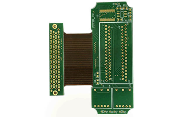
4 layer PCB Stack-up
As a valuable 4 layer PCB stackup supplier, SMTFAB can make custom 4 layer PCB stackup for your projects.
You will see some specifications from our 4 layer PCB stackup. The board thickness is from 0.4mm to 4.0mm, the copper thickness of the outer layer for 4 layer PCB stackup is from 35um to 420um, and the copper thickness of the inner layer is from 18um to 175um.
If you want us to provide a custom 4 layer PCB stackup for your PCB project, you just tell us the board thickness and copper thickness, we will give you our standard 4 layer PCB stackup for your choice.
If you need to manufacture 4 layer PCB and don’t have information for 4 layer PCB stackup, we can help you.

4 layer PCB stackup
Please send your quote to us right now, we will offer the quotation immediately.
4 Layer PCB Stackup: The Ultimate FAQ Guide
Do you know 4 layer PCB stackup? In this guide, you will find information about 4 layer PCB stackup.
Let’s read it now.
- What Is 4 Layer PCB Stackup?
- How Do You Select 4 Layer PCB Stackup?
- How Do You Make 4 Layer PCB Stackup?
- Difference Between Single-layer, Double-Sided, And Multi-Layer (4, 6) Stackup That You Must Know?
- How Do You Use A 4 Layer PCB Stackup?
- How Do You Make 4 Layer PCB Stackup in Altium Design?
- How Do You Make 4 Layer PCB Stackup In Dip Trace?
- What The Thickness Do You Select For A 4 Layer PCB Stackup?
- How Many Layers Does 4 Layer PCB Stackup Has?
- What Are The Best Software To Design 4 Layer PCB Stackup That You May Know?
- Can You Use Calculator For Designing 4 Layer PCB Stackup?
- What Material Do You Use In 4 Layer PCB Stackup?
- What Are Advantages Of 4 Layer PCB Stackup?
- What Are the Disadvantages Of 4 Layer PCB Stackup?
- How Do You Begin Designing 4 Layer PCB Stackup?
- What Are The Types Of Layers In the 4 Layer PCB Stackup That You Should Know?
- What Rules You Should Take Care Of While Designing 4 Layer PCB Stackup?
- How Do You Fabricate 4 Layer PCB Stackup?
- How Do You Calculate The Correct Impedance For 4 Layer PCB Stackup In Altium Design?
- What Technical Challenges Do You Face In Designing 4 Layer PCB Stackup?
- How Do You Know Of The Cost Of 4 Layer PCB Stackup?
- How Do You Know Whether 4 Layer PCB Stackup Is Standard Or Not?
- What Is The Function Of Dielectric Materials In 4 Layer PCB Stackup?
- What Is The Purpose Of Routing Layers In 4 Layer PCB Stackup?
- What Is The Purpose Of Keep Out Layer In 4 Layer PCB Stackup?
- What Purpose Does Split Planes Serve In PCB Stackup?
- How Do You Determine Number Of Layers In 4 Layer PCB Stackup?
- How Do You Determine Layer Arrangement In 4 Layer PCB Stackup?
- How Do You Determine Vias And Routes In 4 Layer PCB Stackup?
- How Do You Determine Type Of Material For Different Layers In 4 Layer PCB Stackup?
What Is 4 Layer PCB Stackup?
Stackup can be defined as the layer’s arrangement of insulators and copper resulting in the manufacturing of the Printed Circuit Board (PCB) before the design of the final board’s layout is decided.
There are two internal layers inside the 4 layer PCB stackup. It depicts that the board is comprising of blind vias too.
Usually, one of these is the ground plane and the other is a signal layer, but there is the possibility for both layers to be of ground planes because of their certain advantages of having ground layers in a parallel way.
There is an alternative for stackup that is having a ground and power plane but is not recommended to have dual internal layers which are in the adjacent scenario to each other.
A certain situation exists where numerous power planes are required. However, certain challenges are limiting the design of PCB stackup.
How Do You Select 4 Layer PCB Stackup?
The number of layers of the printed circuit board (PCB) is depending on the signal and density layers.
You can get an idea of the signal and density layers by looking at fact that a single pin density with 1.0 will be necessitating 2 layers of the signal.
Hence, the required layer number is rising when there is a drop-in pin density.
Similarly, you can have a printed circuit board with over 10 layers when selecting the pin density equivalent to 0.2.

4 layer PCB stackup
How Do You Make 4 Layer PCB Stackup?
The creation of a 4 layer printed circuit board stackup is involving a prepreg layer which is bonding two or many double-sided PCB boards through the application of pressure and heat.
The distinct patterns of conductors that are generated is equating the number of the ultimate layers.
The prepreg is also delivering dielectric among its different layers.
Difference Between Single-layer, Double-Sided, And Multi-Layer (4, 6) Stackup That You Must Know?
The one or single-layered PCB stackup is referring to the circuit boards having only one layer of copper or conductive material.
Such PCBs are manufactured with help of lamination along using an insulating material over the other side of components to be placed onto it for electrical connection and fixing mechanically.
The single layer, double layer PCB stackup is a design having more area of surface for placing components and conducting material such as copper.

2 layer PCB stackup
It can also be mentioned that the surface area is over twice in size when compared to single-layered PCB stackup.
The vias are also placed for the creation of electrical connections for enabling trace routing in order to reach the other side of the board.
While when 3, 4, or more layered PCB stackup are considered, they have more surface area than single and double-layered PCB stackup.
The higher the number of layers, the more is the surface area for traces of conductive material.
The creation of a 4 layer PCB stackup is involving a layer of prepreg which is bonding 2 or more circuit boards through the application of pressure and heat.
The distinct conductive patterns are resulting in the generation of the final layer quantity.

Multilayer PCB stackup
The prepreg layer is also offering dielectric among different layers.
How Do You Use A 4 Layer PCB Stackup?
The 4 layer PCB stackup is one of the most commonly used stack-ups in the contemporary electronics industry.
Such stackup is very simple and is easily fabricated if the basic requirements of layer arrangements and thickness are fulfilled.
The best tool must be used for designing the stackup instead of guessing different factors such as dielectric constant, correct layer count, and loss tangent for defining the PCB.

4 layer PCB
Tools such as Altium designer is offering the best options for creating 4-layer PCB stackup in standard assemblies of multilayer board, rigid-flex boards, and rigid boards.
How Do You Make 4 Layer PCB Stackup in Altium Design?
You should follow the given method in order to design 4 layer PCB stackup in Altium design.
- Load the preset stackup in the Altium design tool through the layer stack manager.
- Select the tool preset.
- Check on 12 layers for creating the default PCB stackup.
- Now, define required layers i.e., 4 layers either as signal or plane layers.
- Other factors and coefficients such as dielectric properties of Df and Dk values can also be managed.
- The weight of the copper layer can also be adjusted right in the menu.
How Do You Make 4 Layer PCB Stackup In Dip Trace?
The following steps are to be followed to make 4 layer PCB stackup in dip trace.
- Route preparation for all components.
- Auto-tracing if manual tracing feels difficult.
- Completing layers work.
- Placing all vias correctly.
- If auto-tracing is applied, look for errors and do manual routing.
- Measuring the length of traces.
- Selection of objects through the layer.
- Placement of graphics and text if any.
- Locking the objects at their specific places.
- Verification of the design.
- Making information of layout.
- Penalizing of the circuit.
- Printing the design.
What The Thickness Do You Select For A 4 Layer PCB Stackup?
The processing of a 4-layer PCB stackup is usually with thickness in various sizes such as 0.125”, 0.093”, 0.062”, 0.047”, 0.040”, 0.031”, and 0.020’’ etc.
The inner layer of PCB may be selected in half, 1, or 2 ounces of copper foil.
The overall size of the PCB stackup is limited to 16×22 inches.

4 layer PCB Thickness
How Many Layers Does 4 Layer PCB Stackup Has?
The 4 layer printed circuit board stackup is having 3 of the single layers and a ground layer making it 4 layers in total.
All these layers are used for the routing of signals.
The first two inner layers are lying inside the core and are often utilized as the power planes or are commonly referred to as routing of signals.
Simply speaking a 4-layer PCB stackup is having 2 of the single, a VCC, and a ground layer.

4 layer PCB stackup
What Are The Best Software To Design 4 Layer PCB Stackup That You May Know?
The following are the best software for designing 4-layer PCB stackup.
- Altium nexus.
- Altium 365 viewer.
- Circuit maker.
- Altium designer.
- Circuit studio.
- DipTrace.
- EagleCAD.
Can You Use Calculator For Designing 4 Layer PCB Stackup?
While making the design of a 4-layer PCB stackup, there is no need of using a calculator.
However, you may use a calculator for computing different factors such as the thickness of copper traces if you need to design a customized PCB stackup.
Similarly, you may also use a calculator for computing the distance among different components to be mechanically affixed to the printed circuit board to enhance its appearance.
Furthermore, the calculator can also be used for the calculation of impedance.
What Material Do You Use In 4 Layer PCB Stackup?
The 4-layer PCB stackup has more than one prepreg and core.
The cores are usually made of laminated sheets of glass-reinforced epoxy that are copper plated.
Usually, the thickness of its core is in the range of 0.1 to 0.3 millimeters.
The prepreg is commonly known as the fabric for reinforcement that is pre-soaked through the resin system.
What Are Advantages Of 4 Layer PCB Stackup?
The following are major advantages of 4 layer PCB stackup that you must know.
- The layers are usually adjacent to ground planes.
The signal that is running over the reference plane having a specific voltage is happening to remain at VCC is supposed to return over the reference plane.
- The layers are having tight contact with all of their adjacent planes.
- All of the ground planes are acting as shields for all of the inner layers.
Better results are expected keeping the traces to the height of the plane as lower as possible.
- Several of the ground planes are lowering the reference or ground plane impedance of PCB and is also reducing the radiation at the common mode.
What Are the Disadvantages Of 4 Layer PCB Stackup?
The following are a few of the disadvantages of 4 layer PCB stackup.
- If the layers of stackup have equal spacing among its current return plane and signal layer, there is a huge separation among its ground and power planes.
Hence, in the case of 4 layer stackup, you cannot correct such deficiencies at the same time so the importance of one must be justified at the start.
- As per normal construction of PCBs, the 4layer stackup is not having enough capacitance among its ground and power plane for enough decoupling.
Therefore, decoupling must be managed and tight coupling must be selected among the current return and signal planes.
- The EMC performance of 4 layer PCB stackup is not up to the mark until the signal layers are placed close to planes.
How Do You Begin Designing 4 Layer PCB Stackup?
You can start building the design of a 4 layer PCB stackup in Altium design through the option of the layer stack manager.
For this you need to go to option “tools”, selecting “preset”, and then check on the 4 layers for the creation of a default stackup Printed Circuit board.
After that, you will be able to define each and every layer according to the signal or plane layer.
You are then also capable of defining the dielectric properties such as values of Df and Dk along with assigning the weights of copper to each layer.
What Are The Types Of Layers In the 4 Layer PCB Stackup That You Should Know?
In a 4-layer PCB stackup design, there are a total of 4 layers.
There are two of the internal layers which are positioned at the core and are usually utilized as the layers for routing of signals or power planes.
Furthermore, there is a layer for grounding and a layer for VCC as well.
What Rules You Should Take Care Of While Designing 4 Layer PCB Stackup?
You need to follow the given rules for designing a high-quality 4 layer PCB stackup.
- Choosing the ground planes in better quality because these are allowing the routing of signals. It also reduces ground impedance and ground noise as well.
- The routing of high-speed signals is required through intermediate layers which are located along with other levels.
This is how ground planes are acting as a shield and is containing all of the radiations that arrive through tracks at higher speeds.
- The layers of signals must be closely located.
- The signal layer must be together with its plane.
- Having many ground planes is of great advantage because these are lowering the ground impedance of the board and are also reducing radiation.
- The mass and power planes must also be thoroughly coupled along.
How Do You Fabricate 4 Layer PCB Stackup?
The following is the procedure you follow for fabricating a 4 layer PCB stackup.
- Cutting the board.
- Cleaning the board.
- Pasting required PCB design onto the board.
- Etching and removal of excess copper from the internal layers to reveal all pads and traces.
- Through lamination creation of PCB stackup with the application of pressure and heat.
- With a drill machine, drilling required holes with vias and pins.
- Again, etching for removal of all excess copper from its surface area for revealing pads and traces.
- Plating of vias and pinholes.
- Addition of protective coating to the surface and then apply solder masking.
- Applying silkscreen and polarity indicators, stickers, and logos if any.
- Adding finishing touches to the copper layers.
- Inspection and testing of the PCB stackup for verification of its proper working.
How Do You Calculate The Correct Impedance For 4 Layer PCB Stackup In Altium Design?
After getting done with the design of 4 layer PCB stackup, you may require to set a specific impedance for the traces.
Usually, the PCB design software is including all of the aspects for setting impedance such as polygons, pads, and vias along with defining feature sizes for ensuring manufacturability and higher signal integrity.
The PCB stackup is determining the routed conductors’ impedances over the surface layer.
The option of integrated field solve of Siberian in Altium designer software is calculating perfect impedance without any use of a calculator or other application.
The targeted impedance of the board is set to be reinforced through the entire routing for making sure that the layout is accurate.
After routing the circuit board, the number of layers is needed to be changed as the Altium designer is automatically adjusting the size of tracks and is adjusting the impedance.
Material properties are utilized along with layer stack manager with real widths of routes for checking the mismatches in impedance and correcting all relevant issues.
What Technical Challenges Do You Face In Designing 4 Layer PCB Stackup?
The following are the major technical challenges that you would face in the design of a 4 layer PCB stackup.
- Having 2 planes for uniform distribution of power in a continuous manner. This is often underneath the surface layers.
- Having trace layers that are in close vicinity to other planes for minimizing and gaining control over impedance and crosstalk.

4 layer PCB stackup
How Do You Know Of The Cost Of 4 Layer PCB Stackup?
The cost of the PCB stackup is greatly affected by the type and quality of material used for its manufacturing.
A typical PCB stackup is laminated with flame retardant 4 (FR4) material.
However, this is not enough for the PCBs which are made for higher intensity use such as the application of fuel and aerospace industry.
Therefore, the cost of the 4 layer PCB stackup is increasing with catering factors such as:
- Thermal reliability.
- Heat transfer.
- Signal performance.
- Temperature reliability.
- Improving mechanical properties.
The cost of a 4 layer PCB stackup is no doubt more than its lesser number of layers PCBs because of its complex design and higher sensitivity.
The distortion of signals is minimized along with a reduction in propagation levels and distortion.
Click here to know about how to reduce PCB design and manufacturing costs.
How Do You Know Whether 4 Layer PCB Stackup Is Standard Or Not?
The standard 4 layer PCB stackup is having a choice of switching its VCC and GND layer with one or more depending on the situation and requirements.
The following are its 4 main layers.
- Signal layer.

- GND layer.

- VCC layer.

- Signal Layer.

What Is The Function Of Dielectric Materials In 4 Layer PCB Stackup?
The dielectric materials are offering two of the critical functions for printed circuit boards as mentioned below.
- The dielectric material is helping in the isolation of signals over the adjacent layers of printed circuit boards.
- The printed circuit board’s stability is highly dependent on the dielectric material’s steady impedance. Usually, it has scattered throughout the plane.
The dielectric material is also monitoring constant impedance through an extensive range of frequencies.
What Is The Purpose Of Routing Layers In 4 Layer PCB Stackup?
The routing layers are found through the external and internal parts of the printed circuit boards.
This is also a layer which designers are taking time to make in a perfect manner.
These layers are very useful for the interconnection of components.
Before the creation of the circuit board, it is of great importance to have routing layers presented to the fabricator.
What Is The Purpose Of Keep Out Layer In 4 Layer PCB Stackup?
The main purpose of the keep-out layer in PCB stackup is to limit the working area of the design of the board.
Therefore, if you are desiring certain specific parts that are drawn at about 3 to 4 inches from PCB’s perimeter, the layer is to limit the entire system in this way.
The keep-out layer is working with the design software and is giving feedback.
It is also helping in the development of the design.
It is also showing any violation that has to happen to the present boundaries.
What Purpose Does Split Planes Serve In PCB Stackup?
The split planes are performing one main function and that is allowing more than a single voltage at a specific layer.
For example, if you are having a certain voltage e.g., 1.1VDC, 6VDC, 11VDC, and 4.5VDC, the plane can be split into distinct copper regions for every voltage on an individual basis.
How Do You Determine Number Of Layers In 4 Layer PCB Stackup?
First and foremost, the step of designing a PCB stackup is to know the number of layers needed.
This step also comprises the consideration of signal, power, plane, or ground layers.
Therefore, it is recommended not to blend different types of signals in the inner layers.
Pin density is utilized for the calculation of an accurate number of layers for PCB stackup design.
The formula for pin density is given below.
After you are done with the calculation of pin density, a lookup table might be utilized for finding the total number of layers required for your PCB stackup.
How Do You Determine Layer Arrangement In 4 Layer PCB Stackup?
When you have the number of layers for your PCB stackup design, you will need to determine the layer arrangement or the way these layers will be stacked.
The following are some tips to do so.
- Routing the higher speed over microstrips of minimum thickness.
- Placing the signal layers adjacent to layers of internal power for solid coupling.
- The ground and power layers must have minimum spacing.
- The two signal layers should be avoided at adjacent collocated places.
- The stackup should be in symmetric position from top to bottom layers in inward.
How Do You Determine Vias And Routes In 4 Layer PCB Stackup?
The PCB stackup design is incomplete without the determination of vias and routes for the traces.
This is also comprising of determination of the weight of copper where the vias are to be put along the type of vias to be implemented.
How Do You Determine Type Of Material For Different Layers In 4 Layer PCB Stackup?
The selection of material for different layers in the PCB stackup is of great importance along with the consideration of thickness for each and every layer.
This has to be recognized in combination with the determination of the core and prepreg thickness.
Certain standard thicknesses and other properties are there for various types of materials of circuit boards.
The selection process is to include material that has a dependency on thermal, mechanical, and electrical properties.
Your Reliable 4 Layer PCB Stackup Manufacturer in China
SMTFAB is a professional 4 layer PCB stackup manufacturer in China, we could provide different types of 4 layer PCB stackup for your project.
- Over 12 years 4 layer PCB stackup design experience
- From 4layer to 40 layer multilayer PCB
- Sufficient raw material in stock to support your orders
- No minimum order quantity for your new order
- Quality guarantee and 100% E-test
- 7/24 sales and engineering tech support
- Production Facility
- Capabilities
| Feature | Capability |
| Quality Grade | Standard IPC 2 and IPC 3 |
| Number of Layers | 2 – 40layers |
| Order Quantity | 1pc – 1Million+pcs |
| Build Time | 24H – 4weeks |
| Material | S1150G, S1165, S1000-2 |
| Board Size | Min 5*5mm | Max 500*650mm |
| Board Thickness | 0.4mm – 6.5mm |
| Copper Weight (Finished) | 0.5oz – 10.0oz |
| Min Tracing/Spacing | 3mil/3mil |
| Solder Mask Sides | As per the file |
| Solder Mask Color | Green, White, Blue, Black, Red, Yellow |
| Silkscreen Sides | As per the file |
| Silkscreen Color | White, Black, Yellow |
| Surface Finish | HASL – Hot Air Solder Leveling |
| Lead-Free HASL – RoHS | |
| ENIG – Electroless Nickle/Immersion Gold – RoHS | |
| Immersion Silver – RoHS | |
| Immersion Tin – RoHS | |
| OSP – Organic Solderability Preservatives – RoHS | |
| Min Annular Ring | 4mil |
| Min Drilling Hole Diameter | 6mil |
| Other Techniques | Gold fingers |
| Blind/Buried Vias |
Releted Some Other PCBs
Why Choose SMTFAB for Your 4 Layer PCB Stackup
SMTFAB has more than 12 years of 4 layer PCB stackup design experience, we’re professional to manufacture 4 layer PCB with the standard stackup. There are four layers as following: Top layer, the bottom layer, VCC, and GND.
Are you looking for a valuable 4 layer PCB stackup manufacturer in China? SMTFAB is your best choice. We have a one-stop turnkey solution for your printed circuit board. SMTFAB can follow your custom 4 layer PCB stackup, meanwhile, we can offer your PCB stackup design, manufacture the prototype to test your designs, and make full service for your large PCB runs.
4 layer PCB Stack-up
As a valuable 4 layer PCB stackup supplier, SMTFAB can make custom 4 layer PCB stackup for your projects.
You will see some specifications from our 4 layer PCB stackup. The board thickness is from 0.4mm to 4.0mm, the copper thickness of the outer layer for 4 layer PCB stackup is from 35um to 420um, and the copper thickness of the inner layer is from 18um to 175um.
If you want us to provide a custom 4 layer PCB stackup for your PCB project, you just tell us the board thickness and copper thickness, we will give you our standard 4 layer PCB stackup for your choice.
If you need to manufacture 4 layer PCB and don’t have information for 4 layer PCB stackup, we can help you.
4 layer PCB stackup
Please send your quote to us right now, we will offer the quotation immediately.
4 Layer PCB Stackup: The Ultimate FAQ Guide
Do you know 4 layer PCB stackup? In this guide, you will find information about 4 layer PCB stackup.
Let’s read it now.
- What Is 4 Layer PCB Stackup?
- How Do You Select 4 Layer PCB Stackup?
- How Do You Make 4 Layer PCB Stackup?
- Difference Between Single-layer, Double-Sided, And Multi-Layer (4, 6) Stackup That You Must Know?
- How Do You Use A 4 Layer PCB Stackup?
- How Do You Make 4 Layer PCB Stackup in Altium Design?
- How Do You Make 4 Layer PCB Stackup In Dip Trace?
- What The Thickness Do You Select For A 4 Layer PCB Stackup?
- How Many Layers Does 4 Layer PCB Stackup Has?
- What Are The Best Software To Design 4 Layer PCB Stackup That You May Know?
- Can You Use Calculator For Designing 4 Layer PCB Stackup?
- What Material Do You Use In 4 Layer PCB Stackup?
- What Are Advantages Of 4 Layer PCB Stackup?
- What Are the Disadvantages Of 4 Layer PCB Stackup?
- How Do You Begin Designing 4 Layer PCB Stackup?
- What Are The Types Of Layers In the 4 Layer PCB Stackup That You Should Know?
- What Rules You Should Take Care Of While Designing 4 Layer PCB Stackup?
- How Do You Fabricate 4 Layer PCB Stackup?
- How Do You Calculate The Correct Impedance For 4 Layer PCB Stackup In Altium Design?
- What Technical Challenges Do You Face In Designing 4 Layer PCB Stackup?
- How Do You Know Of The Cost Of 4 Layer PCB Stackup?
- How Do You Know Whether 4 Layer PCB Stackup Is Standard Or Not?
- What Is The Function Of Dielectric Materials In 4 Layer PCB Stackup?
- What Is The Purpose Of Routing Layers In 4 Layer PCB Stackup?
- What Is The Purpose Of Keep Out Layer In 4 Layer PCB Stackup?
- What Purpose Does Split Planes Serve In PCB Stackup?
- How Do You Determine Number Of Layers In 4 Layer PCB Stackup?
- How Do You Determine Layer Arrangement In 4 Layer PCB Stackup?
- How Do You Determine Vias And Routes In 4 Layer PCB Stackup?
- How Do You Determine Type Of Material For Different Layers In 4 Layer PCB Stackup?
What Is 4 Layer PCB Stackup?
Stackup can be defined as the layer’s arrangement of insulators and copper resulting in the manufacturing of the Printed Circuit Board (PCB) before the design of the final board’s layout is decided.
There are two internal layers inside the 4 layer PCB stackup. It depicts that the board is comprising of blind vias too.
Usually, one of these is the ground plane and the other is a signal layer, but there is the possibility for both layers to be of ground planes because of their certain advantages of having ground layers in a parallel way.
There is an alternative for stackup that is having a ground and power plane but is not recommended to have dual internal layers which are in the adjacent scenario to each other.
A certain situation exists where numerous power planes are required. However, certain challenges are limiting the design of PCB stackup.
How Do You Select 4 Layer PCB Stackup?
The number of layers of the printed circuit board (PCB) is depending on the signal and density layers.
You can get an idea of the signal and density layers by looking at fact that a single pin density with 1.0 will be necessitating 2 layers of the signal.
Hence, the required layer number is rising when there is a drop-in pin density.
Similarly, you can have a printed circuit board with over 10 layers when selecting the pin density equivalent to 0.2.
4 layer PCB stackup
How Do You Make 4 Layer PCB Stackup?
The creation of a 4 layer printed circuit board stackup is involving a prepreg layer which is bonding two or many double-sided PCB boards through the application of pressure and heat.
The distinct patterns of conductors that are generated is equating the number of the ultimate layers.
The prepreg is also delivering dielectric among its different layers.
Difference Between Single-layer, Double-Sided, And Multi-Layer (4, 6) Stackup That You Must Know?
The one or single-layered PCB stackup is referring to the circuit boards having only one layer of copper or conductive material.
Such PCBs are manufactured with help of lamination along using an insulating material over the other side of components to be placed onto it for electrical connection and fixing mechanically.
The single layer, double layer PCB stackup is a design having more area of surface for placing components and conducting material such as copper.
2 layer PCB stackup
It can also be mentioned that the surface area is over twice in size when compared to single-layered PCB stackup.
The vias are also placed for the creation of electrical connections for enabling trace routing in order to reach the other side of the board.
While when 3, 4, or more layered PCB stackup are considered, they have more surface area than single and double-layered PCB stackup.
The higher the number of layers, the more is the surface area for traces of conductive material.
The creation of a 4 layer PCB stackup is involving a layer of prepreg which is bonding 2 or more circuit boards through the application of pressure and heat.
The distinct conductive patterns are resulting in the generation of the final layer quantity.
Multilayer PCB stackup
The prepreg layer is also offering dielectric among different layers.
How Do You Use A 4 Layer PCB Stackup?
The 4 layer PCB stackup is one of the most commonly used stack-ups in the contemporary electronics industry.
Such stackup is very simple and is easily fabricated if the basic requirements of layer arrangements and thickness are fulfilled.
The best tool must be used for designing the stackup instead of guessing different factors such as dielectric constant, correct layer count, and loss tangent for defining the PCB.
4 layer PCB
Tools such as Altium designer is offering the best options for creating 4-layer PCB stackup in standard assemblies of multilayer board, rigid-flex boards, and rigid boards.
How Do You Make 4 Layer PCB Stackup in Altium Design?
You should follow the given method in order to design 4 layer PCB stackup in Altium design.
- Load the preset stackup in the Altium design tool through the layer stack manager.
- Select the tool preset.
- Check on 12 layers for creating the default PCB stackup.
- Now, define required layers i.e., 4 layers either as signal or plane layers.
- Other factors and coefficients such as dielectric properties of Df and Dk values can also be managed.
- The weight of the copper layer can also be adjusted right in the menu.
How Do You Make 4 Layer PCB Stackup In Dip Trace?
The following steps are to be followed to make 4 layer PCB stackup in dip trace.
- Route preparation for all components.
- Auto-tracing if manual tracing feels difficult.
- Completing layers work.
- Placing all vias correctly.
- If auto-tracing is applied, look for errors and do manual routing.
- Measuring the length of traces.
- Selection of objects through the layer.
- Placement of graphics and text if any.
- Locking the objects at their specific places.
- Verification of the design.
- Making information of layout.
- Penalizing of the circuit.
- Printing the design.
What The Thickness Do You Select For A 4 Layer PCB Stackup?
The processing of a 4-layer PCB stackup is usually with thickness in various sizes such as 0.125”, 0.093”, 0.062”, 0.047”, 0.040”, 0.031”, and 0.020’’ etc.
The inner layer of PCB may be selected in half, 1, or 2 ounces of copper foil.
The overall size of the PCB stackup is limited to 16×22 inches.
4 layer PCB Thickness
How Many Layers Does 4 Layer PCB Stackup Has?
The 4 layer printed circuit board stackup is having 3 of the single layers and a ground layer making it 4 layers in total.
All these layers are used for the routing of signals.
The first two inner layers are lying inside the core and are often utilized as the power planes or are commonly referred to as routing of signals.
Simply speaking a 4-layer PCB stackup is having 2 of the single, a VCC, and a ground layer.
4 layer PCB stackup
What Are The Best Software To Design 4 Layer PCB Stackup That You May Know?
The following are the best software for designing 4-layer PCB stackup.
- Altium nexus.
- Altium 365 viewer.
- Circuit maker.
- Altium designer.
- Circuit studio.
- DipTrace.
- EagleCAD.
Can You Use Calculator For Designing 4 Layer PCB Stackup?
While making the design of a 4-layer PCB stackup, there is no need of using a calculator.
However, you may use a calculator for computing different factors such as the thickness of copper traces if you need to design a customized PCB stackup.
Similarly, you may also use a calculator for computing the distance among different components to be mechanically affixed to the printed circuit board to enhance its appearance.
Furthermore, the calculator can also be used for the calculation of impedance.
What Material Do You Use In 4 Layer PCB Stackup?
The 4-layer PCB stackup has more than one prepreg and core.
The cores are usually made of laminated sheets of glass-reinforced epoxy that are copper plated.
Usually, the thickness of its core is in the range of 0.1 to 0.3 millimeters.
The prepreg is commonly known as the fabric for reinforcement that is pre-soaked through the resin system.
What Are Advantages Of 4 Layer PCB Stackup?
The following are major advantages of 4 layer PCB stackup that you must know.
- The layers are usually adjacent to ground planes.
The signal that is running over the reference plane having a specific voltage is happening to remain at VCC is supposed to return over the reference plane.
- The layers are having tight contact with all of their adjacent planes.
- All of the ground planes are acting as shields for all of the inner layers.
Better results are expected keeping the traces to the height of the plane as lower as possible.
- Several of the ground planes are lowering the reference or ground plane impedance of PCB and is also reducing the radiation at the common mode.
What Are the Disadvantages Of 4 Layer PCB Stackup?
The following are a few of the disadvantages of 4 layer PCB stackup.
- If the layers of stackup have equal spacing among its current return plane and signal layer, there is a huge separation among its ground and power planes.
Hence, in the case of 4 layer stackup, you cannot correct such deficiencies at the same time so the importance of one must be justified at the start.
- As per normal construction of PCBs, the 4layer stackup is not having enough capacitance among its ground and power plane for enough decoupling.
Therefore, decoupling must be managed and tight coupling must be selected among the current return and signal planes.
- The EMC performance of 4 layer PCB stackup is not up to the mark until the signal layers are placed close to planes.
How Do You Begin Designing 4 Layer PCB Stackup?
You can start building the design of a 4 layer PCB stackup in Altium design through the option of the layer stack manager.
For this you need to go to option “tools”, selecting “preset”, and then check on the 4 layers for the creation of a default stackup Printed Circuit board.
After that, you will be able to define each and every layer according to the signal or plane layer.
You are then also capable of defining the dielectric properties such as values of Df and Dk along with assigning the weights of copper to each layer.
What Are The Types Of Layers In the 4 Layer PCB Stackup That You Should Know?
In a 4-layer PCB stackup design, there are a total of 4 layers.
There are two of the internal layers which are positioned at the core and are usually utilized as the layers for routing of signals or power planes.
Furthermore, there is a layer for grounding and a layer for VCC as well.
What Rules You Should Take Care Of While Designing 4 Layer PCB Stackup?
You need to follow the given rules for designing a high-quality 4 layer PCB stackup.
- Choosing the ground planes in better quality because these are allowing the routing of signals. It also reduces ground impedance and ground noise as well.
- The routing of high-speed signals is required through intermediate layers which are located along with other levels.
This is how ground planes are acting as a shield and is containing all of the radiations that arrive through tracks at higher speeds.
- The layers of signals must be closely located.
- The signal layer must be together with its plane.
- Having many ground planes is of great advantage because these are lowering the ground impedance of the board and are also reducing radiation.
- The mass and power planes must also be thoroughly coupled along.
How Do You Fabricate 4 Layer PCB Stackup?
The following is the procedure you follow for fabricating a 4 layer PCB stackup.
- Cutting the board.
- Cleaning the board.
- Pasting required PCB design onto the board.
- Etching and removal of excess copper from the internal layers to reveal all pads and traces.
- Through lamination creation of PCB stackup with the application of pressure and heat.
- With a drill machine, drilling required holes with vias and pins.
- Again, etching for removal of all excess copper from its surface area for revealing pads and traces.
- Plating of vias and pinholes.
- Addition of protective coating to the surface and then apply solder masking.
- Applying silkscreen and polarity indicators, stickers, and logos if any.
- Adding finishing touches to the copper layers.
- Inspection and testing of the PCB stackup for verification of its proper working.
How Do You Calculate The Correct Impedance For 4 Layer PCB Stackup In Altium Design?
After getting done with the design of 4 layer PCB stackup, you may require to set a specific impedance for the traces.
Usually, the PCB design software is including all of the aspects for setting impedance such as polygons, pads, and vias along with defining feature sizes for ensuring manufacturability and higher signal integrity.
The PCB stackup is determining the routed conductors’ impedances over the surface layer.
The option of integrated field solve of Siberian in Altium designer software is calculating perfect impedance without any use of a calculator or other application.
The targeted impedance of the board is set to be reinforced through the entire routing for making sure that the layout is accurate.
After routing the circuit board, the number of layers is needed to be changed as the Altium designer is automatically adjusting the size of tracks and is adjusting the impedance.
Material properties are utilized along with layer stack manager with real widths of routes for checking the mismatches in impedance and correcting all relevant issues.
What Technical Challenges Do You Face In Designing 4 Layer PCB Stackup?
The following are the major technical challenges that you would face in the design of a 4 layer PCB stackup.
- Having 2 planes for uniform distribution of power in a continuous manner. This is often underneath the surface layers.
- Having trace layers that are in close vicinity to other planes for minimizing and gaining control over impedance and crosstalk.
4 layer PCB stackup
How Do You Know Of The Cost Of 4 Layer PCB Stackup?
The cost of the PCB stackup is greatly affected by the type and quality of material used for its manufacturing.
A typical PCB stackup is laminated with flame retardant 4 (FR4) material.
However, this is not enough for the PCBs which are made for higher intensity use such as the application of fuel and aerospace industry.
Therefore, the cost of the 4 layer PCB stackup is increasing with catering factors such as:
- Thermal reliability.
- Heat transfer.
- Signal performance.
- Temperature reliability.
- Improving mechanical properties.
The cost of a 4 layer PCB stackup is no doubt more than its lesser number of layers PCBs because of its complex design and higher sensitivity.
The distortion of signals is minimized along with a reduction in propagation levels and distortion.
Click here to know about how to reduce PCB design and manufacturing costs.
How Do You Know Whether 4 Layer PCB Stackup Is Standard Or Not?
The standard 4 layer PCB stackup is having a choice of switching its VCC and GND layer with one or more depending on the situation and requirements.
The following are its 4 main layers.
- Signal layer.
- GND layer.
- VCC layer.
- Signal Layer.
What Is The Function Of Dielectric Materials In 4 Layer PCB Stackup?
The dielectric materials are offering two of the critical functions for printed circuit boards as mentioned below.
- The dielectric material is helping in the isolation of signals over the adjacent layers of printed circuit boards.
- The printed circuit board’s stability is highly dependent on the dielectric material’s steady impedance. Usually, it has scattered throughout the plane.
The dielectric material is also monitoring constant impedance through an extensive range of frequencies.
What Is The Purpose Of Routing Layers In 4 Layer PCB Stackup?
The routing layers are found through the external and internal parts of the printed circuit boards.
This is also a layer which designers are taking time to make in a perfect manner.
These layers are very useful for the interconnection of components.
Before the creation of the circuit board, it is of great importance to have routing layers presented to the fabricator.
What Is The Purpose Of Keep Out Layer In 4 Layer PCB Stackup?
The main purpose of the keep-out layer in PCB stackup is to limit the working area of the design of the board.
Therefore, if you are desiring certain specific parts that are drawn at about 3 to 4 inches from PCB’s perimeter, the layer is to limit the entire system in this way.
The keep-out layer is working with the design software and is giving feedback.
It is also helping in the development of the design.
It is also showing any violation that has to happen to the present boundaries.
What Purpose Does Split Planes Serve In PCB Stackup?
The split planes are performing one main function and that is allowing more than a single voltage at a specific layer.
For example, if you are having a certain voltage e.g., 1.1VDC, 6VDC, 11VDC, and 4.5VDC, the plane can be split into distinct copper regions for every voltage on an individual basis.
How Do You Determine Number Of Layers In 4 Layer PCB Stackup?
First and foremost, the step of designing a PCB stackup is to know the number of layers needed.
This step also comprises the consideration of signal, power, plane, or ground layers.
Therefore, it is recommended not to blend different types of signals in the inner layers.
Pin density is utilized for the calculation of an accurate number of layers for PCB stackup design.
The formula for pin density is given below.
After you are done with the calculation of pin density, a lookup table might be utilized for finding the total number of layers required for your PCB stackup.
How Do You Determine Layer Arrangement In 4 Layer PCB Stackup?
When you have the number of layers for your PCB stackup design, you will need to determine the layer arrangement or the way these layers will be stacked.
The following are some tips to do so.
- Routing the higher speed over microstrips of minimum thickness.
- Placing the signal layers adjacent to layers of internal power for solid coupling.
- The ground and power layers must have minimum spacing.
- The two signal layers should be avoided at adjacent collocated places.
- The stackup should be in symmetric position from top to bottom layers in inward.
How Do You Determine Vias And Routes In 4 Layer PCB Stackup?
The PCB stackup design is incomplete without the determination of vias and routes for the traces.
This is also comprising of determination of the weight of copper where the vias are to be put along the type of vias to be implemented.
How Do You Determine Type Of Material For Different Layers In 4 Layer PCB Stackup?
The selection of material for different layers in the PCB stackup is of great importance along with the consideration of thickness for each and every layer.
This has to be recognized in combination with the determination of the core and prepreg thickness.
Certain standard thicknesses and other properties are there for various types of materials of circuit boards.
The selection process is to include material that has a dependency on thermal, mechanical, and electrical properties.
Your Reliable 4 Layer PCB Stackup Manufacturer in China
SMTFAB is a professional 4 layer PCB stackup manufacturer in China, we could provide different types of 4 layer PCB stackup for your project.
- Over 12 years 4 layer PCB stackup design experience
- From 4layer to 40 layer multilayer PCB
- Sufficient raw material in stock to support your orders
- No minimum order quantity for your new order
- Quality guarantee and 100% E-test
- 7/24 sales and engineering tech support
Your Reliable 4 Layer PCB Stackup Manufacturer in China
Your Reliable 4 Layer PCB Stackup Manufacturer in China
SMTFAB is a professional 4 layer PCB stackup manufacturer in China, we could provide different types of 4 layer PCB stackup for your project.
- Over 12 years 4 layer PCB stackup design experience
- From 4layer to 40 layer multilayer PCB
- Sufficient raw material in stock to support your orders
- No minimum order quantity for your new order
- Quality guarantee and 100% E-test
- 7/24 sales and engineering tech support
- Production Facility
- Capabilities
| Feature | Capability |
| Quality Grade | Standard IPC 2 and IPC 3 |
| Number of Layers | 2 – 40layers |
| Order Quantity | 1pc – 1Million+pcs |
| Build Time | 24H – 4weeks |
| Material | S1150G, S1165, S1000-2 |
| Board Size | Min 5*5mm | Max 500*650mm |
| Board Thickness | 0.4mm – 6.5mm |
| Copper Weight (Finished) | 0.5oz – 10.0oz |
| Min Tracing/Spacing | 3mil/3mil |
| Solder Mask Sides | As per the file |
| Solder Mask Color | Green, White, Blue, Black, Red, Yellow |
| Silkscreen Sides | As per the file |
| Silkscreen Color | White, Black, Yellow |
| Surface Finish | HASL – Hot Air Solder Leveling |
| Lead-Free HASL – RoHS | |
| ENIG – Electroless Nickle/Immersion Gold – RoHS | |
| Immersion Silver – RoHS | |
| Immersion Tin – RoHS | |
| OSP – Organic Solderability Preservatives – RoHS | |
| Min Annular Ring | 4mil |
| Min Drilling Hole Diameter | 6mil |
| Other Techniques | Gold fingers |
| Blind/Buried Vias |
Releted Some Other PCBs
Releted Some Other PCBs
Why Choose SMTFAB for Your 4 Layer PCB Stackup
SMTFAB has more than 12 years of 4 layer PCB stackup design experience, we’re professional to manufacture 4 layer PCB with the standard stackup. There are four layers as following: Top layer, the bottom layer, VCC, and GND.
Are you looking for a valuable 4 layer PCB stackup manufacturer in China? SMTFAB is your best choice. We have a one-stop turnkey solution for your printed circuit board. SMTFAB can follow your custom 4 layer PCB stackup, meanwhile, we can offer your PCB stackup design, manufacture the prototype to test your designs, and make full service for your large PCB runs.
4 layer PCB Stack-up
As a valuable 4 layer PCB stackup supplier, SMTFAB can make custom 4 layer PCB stackup for your projects.
You will see some specifications from our 4 layer PCB stackup. The board thickness is from 0.4mm to 4.0mm, the copper thickness of the outer layer for 4 layer PCB stackup is from 35um to 420um, and the copper thickness of the inner layer is from 18um to 175um.
If you want us to provide a custom 4 layer PCB stackup for your PCB project, you just tell us the board thickness and copper thickness, we will give you our standard 4 layer PCB stackup for your choice.
If you need to manufacture 4 layer PCB and don’t have information for 4 layer PCB stackup, we can help you.
4 layer PCB stackup
Please send your quote to us right now, we will offer the quotation immediately.
4 Layer PCB Stackup: The Ultimate FAQ Guide
Do you know 4 layer PCB stackup? In this guide, you will find information about 4 layer PCB stackup.
Let’s read it now.
- What Is 4 Layer PCB Stackup?
- How Do You Select 4 Layer PCB Stackup?
- How Do You Make 4 Layer PCB Stackup?
- Difference Between Single-layer, Double-Sided, And Multi-Layer (4, 6) Stackup That You Must Know?
- How Do You Use A 4 Layer PCB Stackup?
- How Do You Make 4 Layer PCB Stackup in Altium Design?
- How Do You Make 4 Layer PCB Stackup In Dip Trace?
- What The Thickness Do You Select For A 4 Layer PCB Stackup?
- How Many Layers Does 4 Layer PCB Stackup Has?
- What Are The Best Software To Design 4 Layer PCB Stackup That You May Know?
- Can You Use Calculator For Designing 4 Layer PCB Stackup?
- What Material Do You Use In 4 Layer PCB Stackup?
- What Are Advantages Of 4 Layer PCB Stackup?
- What Are the Disadvantages Of 4 Layer PCB Stackup?
- How Do You Begin Designing 4 Layer PCB Stackup?
- What Are The Types Of Layers In the 4 Layer PCB Stackup That You Should Know?
- What Rules You Should Take Care Of While Designing 4 Layer PCB Stackup?
- How Do You Fabricate 4 Layer PCB Stackup?
- How Do You Calculate The Correct Impedance For 4 Layer PCB Stackup In Altium Design?
- What Technical Challenges Do You Face In Designing 4 Layer PCB Stackup?
- How Do You Know Of The Cost Of 4 Layer PCB Stackup?
- How Do You Know Whether 4 Layer PCB Stackup Is Standard Or Not?
- What Is The Function Of Dielectric Materials In 4 Layer PCB Stackup?
- What Is The Purpose Of Routing Layers In 4 Layer PCB Stackup?
- What Is The Purpose Of Keep Out Layer In 4 Layer PCB Stackup?
- What Purpose Does Split Planes Serve In PCB Stackup?
- How Do You Determine Number Of Layers In 4 Layer PCB Stackup?
- How Do You Determine Layer Arrangement In 4 Layer PCB Stackup?
- How Do You Determine Vias And Routes In 4 Layer PCB Stackup?
- How Do You Determine Type Of Material For Different Layers In 4 Layer PCB Stackup?
What Is 4 Layer PCB Stackup?
Stackup can be defined as the layer’s arrangement of insulators and copper resulting in the manufacturing of the Printed Circuit Board (PCB) before the design of the final board’s layout is decided.
There are two internal layers inside the 4 layer PCB stackup. It depicts that the board is comprising of blind vias too.
Usually, one of these is the ground plane and the other is a signal layer, but there is the possibility for both layers to be of ground planes because of their certain advantages of having ground layers in a parallel way.
There is an alternative for stackup that is having a ground and power plane but is not recommended to have dual internal layers which are in the adjacent scenario to each other.
A certain situation exists where numerous power planes are required. However, certain challenges are limiting the design of PCB stackup.
How Do You Select 4 Layer PCB Stackup?
The number of layers of the printed circuit board (PCB) is depending on the signal and density layers.
You can get an idea of the signal and density layers by looking at fact that a single pin density with 1.0 will be necessitating 2 layers of the signal.
Hence, the required layer number is rising when there is a drop-in pin density.
Similarly, you can have a printed circuit board with over 10 layers when selecting the pin density equivalent to 0.2.
4 layer PCB stackup
How Do You Make 4 Layer PCB Stackup?
The creation of a 4 layer printed circuit board stackup is involving a prepreg layer which is bonding two or many double-sided PCB boards through the application of pressure and heat.
The distinct patterns of conductors that are generated is equating the number of the ultimate layers.
The prepreg is also delivering dielectric among its different layers.
Difference Between Single-layer, Double-Sided, And Multi-Layer (4, 6) Stackup That You Must Know?
The one or single-layered PCB stackup is referring to the circuit boards having only one layer of copper or conductive material.
Such PCBs are manufactured with help of lamination along using an insulating material over the other side of components to be placed onto it for electrical connection and fixing mechanically.
The single layer, double layer PCB stackup is a design having more area of surface for placing components and conducting material such as copper.
2 layer PCB stackup
It can also be mentioned that the surface area is over twice in size when compared to single-layered PCB stackup.
The vias are also placed for the creation of electrical connections for enabling trace routing in order to reach the other side of the board.
While when 3, 4, or more layered PCB stackup are considered, they have more surface area than single and double-layered PCB stackup.
The higher the number of layers, the more is the surface area for traces of conductive material.
The creation of a 4 layer PCB stackup is involving a layer of prepreg which is bonding 2 or more circuit boards through the application of pressure and heat.
The distinct conductive patterns are resulting in the generation of the final layer quantity.
Multilayer PCB stackup
The prepreg layer is also offering dielectric among different layers.
How Do You Use A 4 Layer PCB Stackup?
The 4 layer PCB stackup is one of the most commonly used stack-ups in the contemporary electronics industry.
Such stackup is very simple and is easily fabricated if the basic requirements of layer arrangements and thickness are fulfilled.
The best tool must be used for designing the stackup instead of guessing different factors such as dielectric constant, correct layer count, and loss tangent for defining the PCB.
4 layer PCB
Tools such as Altium designer is offering the best options for creating 4-layer PCB stackup in standard assemblies of multilayer board, rigid-flex boards, and rigid boards.
How Do You Make 4 Layer PCB Stackup in Altium Design?
You should follow the given method in order to design 4 layer PCB stackup in Altium design.
- Load the preset stackup in the Altium design tool through the layer stack manager.
- Select the tool preset.
- Check on 12 layers for creating the default PCB stackup.
- Now, define required layers i.e., 4 layers either as signal or plane layers.
- Other factors and coefficients such as dielectric properties of Df and Dk values can also be managed.
- The weight of the copper layer can also be adjusted right in the menu.
How Do You Make 4 Layer PCB Stackup In Dip Trace?
The following steps are to be followed to make 4 layer PCB stackup in dip trace.
- Route preparation for all components.
- Auto-tracing if manual tracing feels difficult.
- Completing layers work.
- Placing all vias correctly.
- If auto-tracing is applied, look for errors and do manual routing.
- Measuring the length of traces.
- Selection of objects through the layer.
- Placement of graphics and text if any.
- Locking the objects at their specific places.
- Verification of the design.
- Making information of layout.
- Penalizing of the circuit.
- Printing the design.
What The Thickness Do You Select For A 4 Layer PCB Stackup?
The processing of a 4-layer PCB stackup is usually with thickness in various sizes such as 0.125”, 0.093”, 0.062”, 0.047”, 0.040”, 0.031”, and 0.020’’ etc.
The inner layer of PCB may be selected in half, 1, or 2 ounces of copper foil.
The overall size of the PCB stackup is limited to 16×22 inches.
4 layer PCB Thickness
How Many Layers Does 4 Layer PCB Stackup Has?
The 4 layer printed circuit board stackup is having 3 of the single layers and a ground layer making it 4 layers in total.
All these layers are used for the routing of signals.
The first two inner layers are lying inside the core and are often utilized as the power planes or are commonly referred to as routing of signals.
Simply speaking a 4-layer PCB stackup is having 2 of the single, a VCC, and a ground layer.
4 layer PCB stackup
What Are The Best Software To Design 4 Layer PCB Stackup That You May Know?
The following are the best software for designing 4-layer PCB stackup.
- Altium nexus.
- Altium 365 viewer.
- Circuit maker.
- Altium designer.
- Circuit studio.
- DipTrace.
- EagleCAD.
Can You Use Calculator For Designing 4 Layer PCB Stackup?
While making the design of a 4-layer PCB stackup, there is no need of using a calculator.
However, you may use a calculator for computing different factors such as the thickness of copper traces if you need to design a customized PCB stackup.
Similarly, you may also use a calculator for computing the distance among different components to be mechanically affixed to the printed circuit board to enhance its appearance.
Furthermore, the calculator can also be used for the calculation of impedance.
What Material Do You Use In 4 Layer PCB Stackup?
The 4-layer PCB stackup has more than one prepreg and core.
The cores are usually made of laminated sheets of glass-reinforced epoxy that are copper plated.
Usually, the thickness of its core is in the range of 0.1 to 0.3 millimeters.
The prepreg is commonly known as the fabric for reinforcement that is pre-soaked through the resin system.
What Are Advantages Of 4 Layer PCB Stackup?
The following are major advantages of 4 layer PCB stackup that you must know.
- The layers are usually adjacent to ground planes.
The signal that is running over the reference plane having a specific voltage is happening to remain at VCC is supposed to return over the reference plane.
- The layers are having tight contact with all of their adjacent planes.
- All of the ground planes are acting as shields for all of the inner layers.
Better results are expected keeping the traces to the height of the plane as lower as possible.
- Several of the ground planes are lowering the reference or ground plane impedance of PCB and is also reducing the radiation at the common mode.
What Are the Disadvantages Of 4 Layer PCB Stackup?
The following are a few of the disadvantages of 4 layer PCB stackup.
- If the layers of stackup have equal spacing among its current return plane and signal layer, there is a huge separation among its ground and power planes.
Hence, in the case of 4 layer stackup, you cannot correct such deficiencies at the same time so the importance of one must be justified at the start.
- As per normal construction of PCBs, the 4layer stackup is not having enough capacitance among its ground and power plane for enough decoupling.
Therefore, decoupling must be managed and tight coupling must be selected among the current return and signal planes.
- The EMC performance of 4 layer PCB stackup is not up to the mark until the signal layers are placed close to planes.
How Do You Begin Designing 4 Layer PCB Stackup?
You can start building the design of a 4 layer PCB stackup in Altium design through the option of the layer stack manager.
For this you need to go to option “tools”, selecting “preset”, and then check on the 4 layers for the creation of a default stackup Printed Circuit board.
After that, you will be able to define each and every layer according to the signal or plane layer.
You are then also capable of defining the dielectric properties such as values of Df and Dk along with assigning the weights of copper to each layer.
What Are The Types Of Layers In the 4 Layer PCB Stackup That You Should Know?
In a 4-layer PCB stackup design, there are a total of 4 layers.
There are two of the internal layers which are positioned at the core and are usually utilized as the layers for routing of signals or power planes.
Furthermore, there is a layer for grounding and a layer for VCC as well.
What Rules You Should Take Care Of While Designing 4 Layer PCB Stackup?
You need to follow the given rules for designing a high-quality 4 layer PCB stackup.
- Choosing the ground planes in better quality because these are allowing the routing of signals. It also reduces ground impedance and ground noise as well.
- The routing of high-speed signals is required through intermediate layers which are located along with other levels.
This is how ground planes are acting as a shield and is containing all of the radiations that arrive through tracks at higher speeds.
- The layers of signals must be closely located.
- The signal layer must be together with its plane.
- Having many ground planes is of great advantage because these are lowering the ground impedance of the board and are also reducing radiation.
- The mass and power planes must also be thoroughly coupled along.
How Do You Fabricate 4 Layer PCB Stackup?
The following is the procedure you follow for fabricating a 4 layer PCB stackup.
- Cutting the board.
- Cleaning the board.
- Pasting required PCB design onto the board.
- Etching and removal of excess copper from the internal layers to reveal all pads and traces.
- Through lamination creation of PCB stackup with the application of pressure and heat.
- With a drill machine, drilling required holes with vias and pins.
- Again, etching for removal of all excess copper from its surface area for revealing pads and traces.
- Plating of vias and pinholes.
- Addition of protective coating to the surface and then apply solder masking.
- Applying silkscreen and polarity indicators, stickers, and logos if any.
- Adding finishing touches to the copper layers.
- Inspection and testing of the PCB stackup for verification of its proper working.
How Do You Calculate The Correct Impedance For 4 Layer PCB Stackup In Altium Design?
After getting done with the design of 4 layer PCB stackup, you may require to set a specific impedance for the traces.
Usually, the PCB design software is including all of the aspects for setting impedance such as polygons, pads, and vias along with defining feature sizes for ensuring manufacturability and higher signal integrity.
The PCB stackup is determining the routed conductors’ impedances over the surface layer.
The option of integrated field solve of Siberian in Altium designer software is calculating perfect impedance without any use of a calculator or other application.
The targeted impedance of the board is set to be reinforced through the entire routing for making sure that the layout is accurate.
After routing the circuit board, the number of layers is needed to be changed as the Altium designer is automatically adjusting the size of tracks and is adjusting the impedance.
Material properties are utilized along with layer stack manager with real widths of routes for checking the mismatches in impedance and correcting all relevant issues.
What Technical Challenges Do You Face In Designing 4 Layer PCB Stackup?
The following are the major technical challenges that you would face in the design of a 4 layer PCB stackup.
- Having 2 planes for uniform distribution of power in a continuous manner. This is often underneath the surface layers.
- Having trace layers that are in close vicinity to other planes for minimizing and gaining control over impedance and crosstalk.
4 layer PCB stackup
How Do You Know Of The Cost Of 4 Layer PCB Stackup?
The cost of the PCB stackup is greatly affected by the type and quality of material used for its manufacturing.
A typical PCB stackup is laminated with flame retardant 4 (FR4) material.
However, this is not enough for the PCBs which are made for higher intensity use such as the application of fuel and aerospace industry.
Therefore, the cost of the 4 layer PCB stackup is increasing with catering factors such as:
- Thermal reliability.
- Heat transfer.
- Signal performance.
- Temperature reliability.
- Improving mechanical properties.
The cost of a 4 layer PCB stackup is no doubt more than its lesser number of layers PCBs because of its complex design and higher sensitivity.
The distortion of signals is minimized along with a reduction in propagation levels and distortion.
Click here to know about how to reduce PCB design and manufacturing costs.
How Do You Know Whether 4 Layer PCB Stackup Is Standard Or Not?
The standard 4 layer PCB stackup is having a choice of switching its VCC and GND layer with one or more depending on the situation and requirements.
The following are its 4 main layers.
- Signal layer.
- GND layer.
- VCC layer.
- Signal Layer.
What Is The Function Of Dielectric Materials In 4 Layer PCB Stackup?
The dielectric materials are offering two of the critical functions for printed circuit boards as mentioned below.
- The dielectric material is helping in the isolation of signals over the adjacent layers of printed circuit boards.
- The printed circuit board’s stability is highly dependent on the dielectric material’s steady impedance. Usually, it has scattered throughout the plane.
The dielectric material is also monitoring constant impedance through an extensive range of frequencies.
What Is The Purpose Of Routing Layers In 4 Layer PCB Stackup?
The routing layers are found through the external and internal parts of the printed circuit boards.
This is also a layer which designers are taking time to make in a perfect manner.
These layers are very useful for the interconnection of components.
Before the creation of the circuit board, it is of great importance to have routing layers presented to the fabricator.
What Is The Purpose Of Keep Out Layer In 4 Layer PCB Stackup?
The main purpose of the keep-out layer in PCB stackup is to limit the working area of the design of the board.
Therefore, if you are desiring certain specific parts that are drawn at about 3 to 4 inches from PCB’s perimeter, the layer is to limit the entire system in this way.
The keep-out layer is working with the design software and is giving feedback.
It is also helping in the development of the design.
It is also showing any violation that has to happen to the present boundaries.
What Purpose Does Split Planes Serve In PCB Stackup?
The split planes are performing one main function and that is allowing more than a single voltage at a specific layer.
For example, if you are having a certain voltage e.g., 1.1VDC, 6VDC, 11VDC, and 4.5VDC, the plane can be split into distinct copper regions for every voltage on an individual basis.
How Do You Determine Number Of Layers In 4 Layer PCB Stackup?
First and foremost, the step of designing a PCB stackup is to know the number of layers needed.
This step also comprises the consideration of signal, power, plane, or ground layers.
Therefore, it is recommended not to blend different types of signals in the inner layers.
Pin density is utilized for the calculation of an accurate number of layers for PCB stackup design.
The formula for pin density is given below.
After you are done with the calculation of pin density, a lookup table might be utilized for finding the total number of layers required for your PCB stackup.
How Do You Determine Layer Arrangement In 4 Layer PCB Stackup?
When you have the number of layers for your PCB stackup design, you will need to determine the layer arrangement or the way these layers will be stacked.
The following are some tips to do so.
- Routing the higher speed over microstrips of minimum thickness.
- Placing the signal layers adjacent to layers of internal power for solid coupling.
- The ground and power layers must have minimum spacing.
- The two signal layers should be avoided at adjacent collocated places.
- The stackup should be in symmetric position from top to bottom layers in inward.
How Do You Determine Vias And Routes In 4 Layer PCB Stackup?
The PCB stackup design is incomplete without the determination of vias and routes for the traces.
This is also comprising of determination of the weight of copper where the vias are to be put along the type of vias to be implemented.
How Do You Determine Type Of Material For Different Layers In 4 Layer PCB Stackup?
The selection of material for different layers in the PCB stackup is of great importance along with the consideration of thickness for each and every layer.
This has to be recognized in combination with the determination of the core and prepreg thickness.
Certain standard thicknesses and other properties are there for various types of materials of circuit boards.
The selection process is to include material that has a dependency on thermal, mechanical, and electrical properties.
Why Choose SMTFAB for Your 4 Layer PCB Stackup
SMTFAB has more than 12 years of 4 layer PCB stackup design experience, we’re professional to manufacture 4 layer PCB with the standard stackup. There are four layers as following: Top layer, the bottom layer, VCC, and GND.
Are you looking for a valuable 4 layer PCB stackup manufacturer in China? SMTFAB is your best choice. We have a one-stop turnkey solution for your printed circuit board. SMTFAB can follow your custom 4 layer PCB stackup, meanwhile, we can offer your PCB stackup design, manufacture the prototype to test your designs, and make full service for your large PCB runs.
As a valuable 4 layer PCB stackup supplier, SMTFAB can make custom 4 layer PCB stackup for your projects.
You will see some specifications from our 4 layer PCB stackup. The board thickness is from 0.4mm to 4.0mm, the copper thickness of the outer layer for 4 layer PCB stackup is from 35um to 420um, and the copper thickness of the inner layer is from 18um to 175um.
If you want us to provide a custom 4 layer PCB stackup for your PCB project, you just tell us the board thickness and copper thickness, we will give you our standard 4 layer PCB stackup for your choice.
If you need to manufacture 4 layer PCB and don’t have information for 4 layer PCB stackup, we can help you.
Please send your quote to us right now, we will offer the quotation immediately.
4 Layer PCB Stackup: The Ultimate FAQ Guide
Do you know 4 layer PCB stackup? In this guide, you will find information about 4 layer PCB stackup.
- What Is 4 Layer PCB Stackup?
- How Do You Select 4 Layer PCB Stackup?
- How Do You Make 4 Layer PCB Stackup?
- Difference Between Single-layer, Double-Sided, And Multi-Layer (4, 6) Stackup That You Must Know?
- How Do You Use A 4 Layer PCB Stackup?
- How Do You Make 4 Layer PCB Stackup in Altium Design?
- How Do You Make 4 Layer PCB Stackup In Dip Trace?
- What The Thickness Do You Select For A 4 Layer PCB Stackup?
- How Many Layers Does 4 Layer PCB Stackup Has?
- What Are The Best Software To Design 4 Layer PCB Stackup That You May Know?
- Can You Use Calculator For Designing 4 Layer PCB Stackup?
- What Material Do You Use In 4 Layer PCB Stackup?
- What Are Advantages Of 4 Layer PCB Stackup?
- What Are the Disadvantages Of 4 Layer PCB Stackup?
- How Do You Begin Designing 4 Layer PCB Stackup?
- What Are The Types Of Layers In the 4 Layer PCB Stackup That You Should Know?
- What Rules You Should Take Care Of While Designing 4 Layer PCB Stackup?
- How Do You Fabricate 4 Layer PCB Stackup?
- How Do You Calculate The Correct Impedance For 4 Layer PCB Stackup In Altium Design?
- What Technical Challenges Do You Face In Designing 4 Layer PCB Stackup?
- How Do You Know Of The Cost Of 4 Layer PCB Stackup?
- How Do You Know Whether 4 Layer PCB Stackup Is Standard Or Not?
- What Is The Function Of Dielectric Materials In 4 Layer PCB Stackup?
- What Is The Purpose Of Routing Layers In 4 Layer PCB Stackup?
- What Is The Purpose Of Keep Out Layer In 4 Layer PCB Stackup?
- What Purpose Does Split Planes Serve In PCB Stackup?
- How Do You Determine Number Of Layers In 4 Layer PCB Stackup?
- How Do You Determine Layer Arrangement In 4 Layer PCB Stackup?
- How Do You Determine Vias And Routes In 4 Layer PCB Stackup?
- How Do You Determine Type Of Material For Different Layers In 4 Layer PCB Stackup?
What Is 4 Layer PCB Stackup?
Stackup can be defined as the layer’s arrangement of insulators and copper resulting in the manufacturing of the Printed Circuit Board (PCB) before the design of the final board’s layout is decided.
There are two internal layers inside the 4 layer PCB stackup. It depicts that the board is comprising of blind vias too.
Usually, one of these is the ground plane and the other is a signal layer, but there is the possibility for both layers to be of ground planes because of their certain advantages of having ground layers in a parallel way.
There is an alternative for stackup that is having a ground and power plane but is not recommended to have dual internal layers which are in the adjacent scenario to each other.
A certain situation exists where numerous power planes are required. However, certain challenges are limiting the design of PCB stackup.
How Do You Select 4 Layer PCB Stackup?
The number of layers of the printed circuit board (PCB) is depending on the signal and density layers.
You can get an idea of the signal and density layers by looking at fact that a single pin density with 1.0 will be necessitating 2 layers of the signal.
Hence, the required layer number is rising when there is a drop-in pin density.
Similarly, you can have a printed circuit board with over 10 layers when selecting the pin density equivalent to 0.2.
How Do You Make 4 Layer PCB Stackup?
The creation of a 4 layer printed circuit board stackup is involving a prepreg layer which is bonding two or many double-sided PCB boards through the application of pressure and heat.
The distinct patterns of conductors that are generated is equating the number of the ultimate layers.
The prepreg is also delivering dielectric among its different layers.
Difference Between Single-layer, Double-Sided, And Multi-Layer (4, 6) Stackup That You Must Know?
The one or single-layered PCB stackup is referring to the circuit boards having only one layer of copper or conductive material.
Such PCBs are manufactured with help of lamination along using an insulating material over the other side of components to be placed onto it for electrical connection and fixing mechanically.
The single layer, double layer PCB stackup is a design having more area of surface for placing components and conducting material such as copper.
It can also be mentioned that the surface area is over twice in size when compared to single-layered PCB stackup.
The vias are also placed for the creation of electrical connections for enabling trace routing in order to reach the other side of the board.
While when 3, 4, or more layered PCB stackup are considered, they have more surface area than single and double-layered PCB stackup.
The higher the number of layers, the more is the surface area for traces of conductive material.
The creation of a 4 layer PCB stackup is involving a layer of prepreg which is bonding 2 or more circuit boards through the application of pressure and heat.
The distinct conductive patterns are resulting in the generation of the final layer quantity.
Multilayer PCB stackup
The prepreg layer is also offering dielectric among different layers.
How Do You Use A 4 Layer PCB Stackup?
The 4 layer PCB stackup is one of the most commonly used stack-ups in the contemporary electronics industry.
Such stackup is very simple and is easily fabricated if the basic requirements of layer arrangements and thickness are fulfilled.
The best tool must be used for designing the stackup instead of guessing different factors such as dielectric constant, correct layer count, and loss tangent for defining the PCB.
Tools such as Altium designer is offering the best options for creating 4-layer PCB stackup in standard assemblies of multilayer board, rigid-flex boards, and rigid boards.
How Do You Make 4 Layer PCB Stackup in Altium Design?
You should follow the given method in order to design 4 layer PCB stackup in Altium design.
- Load the preset stackup in the Altium design tool through the layer stack manager.
- Select the tool preset.
- Check on 12 layers for creating the default PCB stackup.
- Now, define required layers i.e., 4 layers either as signal or plane layers.
- Other factors and coefficients such as dielectric properties of Df and Dk values can also be managed.
- The weight of the copper layer can also be adjusted right in the menu.
How Do You Make 4 Layer PCB Stackup In Dip Trace?
The following steps are to be followed to make 4 layer PCB stackup in dip trace.
- Route preparation for all components.
- Auto-tracing if manual tracing feels difficult.
- Completing layers work.
- Placing all vias correctly.
- If auto-tracing is applied, look for errors and do manual routing.
- Measuring the length of traces.
- Selection of objects through the layer.
- Placement of graphics and text if any.
- Locking the objects at their specific places.
- Verification of the design.
- Making information of layout.
- Penalizing of the circuit.
- Printing the design.
What The Thickness Do You Select For A 4 Layer PCB Stackup?
The processing of a 4-layer PCB stackup is usually with thickness in various sizes such as 0.125”, 0.093”, 0.062”, 0.047”, 0.040”, 0.031”, and 0.020’’ etc.
The inner layer of PCB may be selected in half, 1, or 2 ounces of copper foil.
The overall size of the PCB stackup is limited to 16×22 inches.
4 layer PCB Thickness
How Many Layers Does 4 Layer PCB Stackup Has?
The 4 layer printed circuit board stackup is having 3 of the single layers and a ground layer making it 4 layers in total.
All these layers are used for the routing of signals.
The first two inner layers are lying inside the core and are often utilized as the power planes or are commonly referred to as routing of signals.
Simply speaking a 4-layer PCB stackup is having 2 of the single, a VCC, and a ground layer.
What Are The Best Software To Design 4 Layer PCB Stackup That You May Know?
The following are the best software for designing 4-layer PCB stackup.
- Altium nexus.
- Altium 365 viewer.
- Circuit maker.
- Altium designer.
- Circuit studio.
- DipTrace.
- EagleCAD.
Can You Use Calculator For Designing 4 Layer PCB Stackup?
While making the design of a 4-layer PCB stackup, there is no need of using a calculator.
However, you may use a calculator for computing different factors such as the thickness of copper traces if you need to design a customized PCB stackup.
Similarly, you may also use a calculator for computing the distance among different components to be mechanically affixed to the printed circuit board to enhance its appearance.
Furthermore, the calculator can also be used for the calculation of impedance.
What Material Do You Use In 4 Layer PCB Stackup?
The 4-layer PCB stackup has more than one prepreg and core.
The cores are usually made of laminated sheets of glass-reinforced epoxy that are copper plated.
Usually, the thickness of its core is in the range of 0.1 to 0.3 millimeters.
The prepreg is commonly known as the fabric for reinforcement that is pre-soaked through the resin system.
What Are Advantages Of 4 Layer PCB Stackup?
The following are major advantages of 4 layer PCB stackup that you must know.
- The layers are usually adjacent to ground planes.
The signal that is running over the reference plane having a specific voltage is happening to remain at VCC is supposed to return over the reference plane.
- The layers are having tight contact with all of their adjacent planes.
- All of the ground planes are acting as shields for all of the inner layers.
Better results are expected keeping the traces to the height of the plane as lower as possible.
- Several of the ground planes are lowering the reference or ground plane impedance of PCB and is also reducing the radiation at the common mode.
What Are the Disadvantages Of 4 Layer PCB Stackup?
The following are a few of the disadvantages of 4 layer PCB stackup.
- If the layers of stackup have equal spacing among its current return plane and signal layer, there is a huge separation among its ground and power planes.
Hence, in the case of 4 layer stackup, you cannot correct such deficiencies at the same time so the importance of one must be justified at the start.
- As per normal construction of PCBs, the 4layer stackup is not having enough capacitance among its ground and power plane for enough decoupling.
Therefore, decoupling must be managed and tight coupling must be selected among the current return and signal planes.
- The EMC performance of 4 layer PCB stackup is not up to the mark until the signal layers are placed close to planes.
How Do You Begin Designing 4 Layer PCB Stackup?
You can start building the design of a 4 layer PCB stackup in Altium design through the option of the layer stack manager.
For this you need to go to option “tools”, selecting “preset”, and then check on the 4 layers for the creation of a default stackup Printed Circuit board.
After that, you will be able to define each and every layer according to the signal or plane layer.
You are then also capable of defining the dielectric properties such as values of Df and Dk along with assigning the weights of copper to each layer.
What Are The Types Of Layers In the 4 Layer PCB Stackup That You Should Know?
In a 4-layer PCB stackup design, there are a total of 4 layers.
There are two of the internal layers which are positioned at the core and are usually utilized as the layers for routing of signals or power planes.
Furthermore, there is a layer for grounding and a layer for VCC as well.
What Rules You Should Take Care Of While Designing 4 Layer PCB Stackup?
You need to follow the given rules for designing a high-quality 4 layer PCB stackup.
- Choosing the ground planes in better quality because these are allowing the routing of signals. It also reduces ground impedance and ground noise as well.
- The routing of high-speed signals is required through intermediate layers which are located along with other levels.
This is how ground planes are acting as a shield and is containing all of the radiations that arrive through tracks at higher speeds.
- The layers of signals must be closely located.
- The signal layer must be together with its plane.
- Having many ground planes is of great advantage because these are lowering the ground impedance of the board and are also reducing radiation.
- The mass and power planes must also be thoroughly coupled along.
How Do You Fabricate 4 Layer PCB Stackup?
The following is the procedure you follow for fabricating a 4 layer PCB stackup.
- Cutting the board.
- Cleaning the board.
- Pasting required PCB design onto the board.
- Etching and removal of excess copper from the internal layers to reveal all pads and traces.
- Through lamination creation of PCB stackup with the application of pressure and heat.
- With a drill machine, drilling required holes with vias and pins.
- Again, etching for removal of all excess copper from its surface area for revealing pads and traces.
- Plating of vias and pinholes.
- Addition of protective coating to the surface and then apply solder masking.
- Applying silkscreen and polarity indicators, stickers, and logos if any.
- Adding finishing touches to the copper layers.
- Inspection and testing of the PCB stackup for verification of its proper working.
How Do You Calculate The Correct Impedance For 4 Layer PCB Stackup In Altium Design?
After getting done with the design of 4 layer PCB stackup, you may require to set a specific impedance for the traces.
Usually, the PCB design software is including all of the aspects for setting impedance such as polygons, pads, and vias along with defining feature sizes for ensuring manufacturability and higher signal integrity.
The PCB stackup is determining the routed conductors’ impedances over the surface layer.
The option of integrated field solve of Siberian in Altium designer software is calculating perfect impedance without any use of a calculator or other application.
The targeted impedance of the board is set to be reinforced through the entire routing for making sure that the layout is accurate.
After routing the circuit board, the number of layers is needed to be changed as the Altium designer is automatically adjusting the size of tracks and is adjusting the impedance.
Material properties are utilized along with layer stack manager with real widths of routes for checking the mismatches in impedance and correcting all relevant issues.
What Technical Challenges Do You Face In Designing 4 Layer PCB Stackup?
The following are the major technical challenges that you would face in the design of a 4 layer PCB stackup.
- Having 2 planes for uniform distribution of power in a continuous manner. This is often underneath the surface layers.
- Having trace layers that are in close vicinity to other planes for minimizing and gaining control over impedance and crosstalk.
How Do You Know Of The Cost Of 4 Layer PCB Stackup?
The cost of the PCB stackup is greatly affected by the type and quality of material used for its manufacturing.
A typical PCB stackup is laminated with flame retardant 4 (FR4) material.
However, this is not enough for the PCBs which are made for higher intensity use such as the application of fuel and aerospace industry.
Therefore, the cost of the 4 layer PCB stackup is increasing with catering factors such as:
- Thermal reliability.
- Heat transfer.
- Signal performance.
- Temperature reliability.
- Improving mechanical properties.
The cost of a 4 layer PCB stackup is no doubt more than its lesser number of layers PCBs because of its complex design and higher sensitivity.
The distortion of signals is minimized along with a reduction in propagation levels and distortion.
Click here to know about how to reduce PCB design and manufacturing costs.
How Do You Know Whether 4 Layer PCB Stackup Is Standard Or Not?
The standard 4 layer PCB stackup is having a choice of switching its VCC and GND layer with one or more depending on the situation and requirements.
The following are its 4 main layers.
What Is The Function Of Dielectric Materials In 4 Layer PCB Stackup?
The dielectric materials are offering two of the critical functions for printed circuit boards as mentioned below.
- The dielectric material is helping in the isolation of signals over the adjacent layers of printed circuit boards.
- The printed circuit board’s stability is highly dependent on the dielectric material’s steady impedance. Usually, it has scattered throughout the plane.
The dielectric material is also monitoring constant impedance through an extensive range of frequencies.
What Is The Purpose Of Routing Layers In 4 Layer PCB Stackup?
The routing layers are found through the external and internal parts of the printed circuit boards.
This is also a layer which designers are taking time to make in a perfect manner.
These layers are very useful for the interconnection of components.
Before the creation of the circuit board, it is of great importance to have routing layers presented to the fabricator.
What Is The Purpose Of Keep Out Layer In 4 Layer PCB Stackup?
The main purpose of the keep-out layer in PCB stackup is to limit the working area of the design of the board.
Therefore, if you are desiring certain specific parts that are drawn at about 3 to 4 inches from PCB’s perimeter, the layer is to limit the entire system in this way.
The keep-out layer is working with the design software and is giving feedback.
It is also helping in the development of the design.
It is also showing any violation that has to happen to the present boundaries.
What Purpose Does Split Planes Serve In PCB Stackup?
The split planes are performing one main function and that is allowing more than a single voltage at a specific layer.
For example, if you are having a certain voltage e.g., 1.1VDC, 6VDC, 11VDC, and 4.5VDC, the plane can be split into distinct copper regions for every voltage on an individual basis.
How Do You Determine Number Of Layers In 4 Layer PCB Stackup?
First and foremost, the step of designing a PCB stackup is to know the number of layers needed.
This step also comprises the consideration of signal, power, plane, or ground layers.
Therefore, it is recommended not to blend different types of signals in the inner layers.
Pin density is utilized for the calculation of an accurate number of layers for PCB stackup design.
The formula for pin density is given below.
After you are done with the calculation of pin density, a lookup table might be utilized for finding the total number of layers required for your PCB stackup.
How Do You Determine Layer Arrangement In 4 Layer PCB Stackup?
When you have the number of layers for your PCB stackup design, you will need to determine the layer arrangement or the way these layers will be stacked.
The following are some tips to do so.
- Routing the higher speed over microstrips of minimum thickness.
- Placing the signal layers adjacent to layers of internal power for solid coupling.
- The ground and power layers must have minimum spacing.
- The two signal layers should be avoided at adjacent collocated places.
- The stackup should be in symmetric position from top to bottom layers in inward.
How Do You Determine Vias And Routes In 4 Layer PCB Stackup?
The PCB stackup design is incomplete without the determination of vias and routes for the traces.
This is also comprising of determination of the weight of copper where the vias are to be put along the type of vias to be implemented.
How Do You Determine Type Of Material For Different Layers In 4 Layer PCB Stackup?
The selection of material for different layers in the PCB stackup is of great importance along with the consideration of thickness for each and every layer.
This has to be recognized in combination with the determination of the core and prepreg thickness.
Certain standard thicknesses and other properties are there for various types of materials of circuit boards.
The selection process is to include material that has a dependency on thermal, mechanical, and electrical properties.
Technical Specifications
| 0 | { |
| 1 | " |
| 2 | F |
| 3 | e |
| 4 | a |
| 5 | t |
| 6 | u |
| 7 | r |
| 8 | e |
| 9 | " |
| 10 | : |
| 11 | " |
| 12 | C |
| 13 | a |
| 14 | p |
| 15 | a |
| 16 | b |
| 17 | i |
| 18 | l |
| 19 | i |
| 20 | t |
| 21 | y |
| 22 | " |
| 23 | , |
| 24 | " |
| 25 | Q |
| 26 | u |
| 27 | a |
| 28 | l |
| 29 | i |
| 30 | t |
| 31 | y |
| 32 | |
| 33 | G |
| 34 | r |
| 35 | a |
| 36 | d |
| 37 | e |
| 38 | " |
| 39 | : |
| 40 | " |
| 41 | S |
| 42 | t |
| 43 | a |
| 44 | n |
| 45 | d |
| 46 | a |
| 47 | r |
| 48 | d |
| 49 | |
| 50 | I |
| 51 | P |
| 52 | C |
| 53 | |
| 54 | 2 |
| 55 | |
| 56 | a |
| 57 | n |
| 58 | d |
| 59 | |
| 60 | I |
| 61 | P |
| 62 | C |
| 63 | |
| 64 | 3 |
| 65 | " |
| 66 | , |
| 67 | " |
| 68 | N |
| 69 | u |
| 70 | m |
| 71 | b |
| 72 | e |
| 73 | r |
| 74 | |
| 75 | o |
| 76 | f |
| 77 | |
| 78 | L |
| 79 | a |
| 80 | y |
| 81 | e |
| 82 | r |
| 83 | s |
| 84 | " |
| 85 | : |
| 86 | " |
| 87 | 2 |
| 88 | |
| 89 | – |
| 90 | |
| 91 | 4 |
| 92 | 0 |
| 93 | l |
| 94 | a |
| 95 | y |
| 96 | e |
| 97 | r |
| 98 | s |
| 99 | " |
| 100 | , |
| 101 | " |
| 102 | O |
| 103 | r |
| 104 | d |
| 105 | e |
| 106 | r |
| 107 | |
| 108 | Q |
| 109 | u |
| 110 | a |
| 111 | n |
| 112 | t |
| 113 | i |
| 114 | t |
| 115 | y |
| 116 | " |
| 117 | : |
| 118 | " |
| 119 | 1 |
| 120 | p |
| 121 | c |
| 122 | |
| 123 | – |
| 124 | |
| 125 | 1 |
| 126 | M |
| 127 | i |
| 128 | l |
| 129 | l |
| 130 | i |
| 131 | o |
| 132 | n |
| 133 | + |
| 134 | p |
| 135 | c |
| 136 | s |
| 137 | " |
| 138 | , |
| 139 | " |
| 140 | B |
| 141 | u |
| 142 | i |
| 143 | l |
| 144 | d |
| 145 | |
| 146 | T |
| 147 | i |
| 148 | m |
| 149 | e |
| 150 | " |
| 151 | : |
| 152 | " |
| 153 | 2 |
| 154 | 4 |
| 155 | H |
| 156 | |
| 157 | – |
| 158 | |
| 159 | 4 |
| 160 | w |
| 161 | e |
| 162 | e |
| 163 | k |
| 164 | s |
| 165 | " |
| 166 | , |
| 167 | " |
| 168 | M |
| 169 | a |
| 170 | t |
| 171 | e |
| 172 | r |
| 173 | i |
| 174 | a |
| 175 | l |
| 176 | " |
| 177 | : |
| 178 | " |
| 179 | S |
| 180 | 1 |
| 181 | 1 |
| 182 | 5 |
| 183 | 0 |
| 184 | G |
| 185 | , |
| 186 | |
| 187 | S |
| 188 | 1 |
| 189 | 1 |
| 190 | 6 |
| 191 | 5 |
| 192 | , |
| 193 | |
| 194 | S |
| 195 | 1 |
| 196 | 0 |
| 197 | 0 |
| 198 | 0 |
| 199 | - |
| 200 | 2 |
| 201 | " |
| 202 | , |
| 203 | " |
| 204 | B |
| 205 | o |
| 206 | a |
| 207 | r |
| 208 | d |
| 209 | |
| 210 | S |
| 211 | i |
| 212 | z |
| 213 | e |
| 214 | " |
| 215 | : |
| 216 | " |
| 217 | M |
| 218 | i |
| 219 | n |
| 220 | |
| 221 | 5 |
| 222 | * |
| 223 | 5 |
| 224 | m |
| 225 | m |
| 226 | |
| 227 | | |
| 228 | |
| 229 | M |
| 230 | a |
| 231 | x |
| 232 | |
| 233 | 5 |
| 234 | 0 |
| 235 | 0 |
| 236 | * |
| 237 | 6 |
| 238 | 5 |
| 239 | 0 |
| 240 | m |
| 241 | m |
| 242 | " |
| 243 | , |
| 244 | " |
| 245 | B |
| 246 | o |
| 247 | a |
| 248 | r |
| 249 | d |
| 250 | |
| 251 | T |
| 252 | h |
| 253 | i |
| 254 | c |
| 255 | k |
| 256 | n |
| 257 | e |
| 258 | s |
| 259 | s |
| 260 | " |
| 261 | : |
| 262 | " |
| 263 | 0 |
| 264 | . |
| 265 | 4 |
| 266 | m |
| 267 | m |
| 268 | |
| 269 | – |
| 270 | |
| 271 | 6 |
| 272 | . |
| 273 | 5 |
| 274 | m |
| 275 | m |
| 276 | " |
| 277 | , |
| 278 | " |
| 279 | C |
| 280 | o |
| 281 | p |
| 282 | p |
| 283 | e |
| 284 | r |
| 285 | |
| 286 | W |
| 287 | e |
| 288 | i |
| 289 | g |
| 290 | h |
| 291 | t |
| 292 | |
| 293 | ( |
| 294 | F |
| 295 | i |
| 296 | n |
| 297 | i |
| 298 | s |
| 299 | h |
| 300 | e |
| 301 | d |
| 302 | ) |
| 303 | " |
| 304 | : |
| 305 | " |
| 306 | 0 |
| 307 | . |
| 308 | 5 |
| 309 | o |
| 310 | z |
| 311 | |
| 312 | – |
| 313 | |
| 314 | 1 |
| 315 | 0 |
| 316 | . |
| 317 | 0 |
| 318 | o |
| 319 | z |
| 320 | " |
| 321 | , |
| 322 | " |
| 323 | M |
| 324 | i |
| 325 | n |
| 326 | |
| 327 | T |
| 328 | r |
| 329 | a |
| 330 | c |
| 331 | i |
| 332 | n |
| 333 | g |
| 334 | / |
| 335 | S |
| 336 | p |
| 337 | a |
| 338 | c |
| 339 | i |
| 340 | n |
| 341 | g |
| 342 | " |
| 343 | : |
| 344 | " |
| 345 | 3 |
| 346 | m |
| 347 | i |
| 348 | l |
| 349 | / |
| 350 | 3 |
| 351 | m |
| 352 | i |
| 353 | l |
| 354 | " |
| 355 | , |
| 356 | " |
| 357 | S |
| 358 | o |
| 359 | l |
| 360 | d |
| 361 | e |
| 362 | r |
| 363 | |
| 364 | M |
| 365 | a |
| 366 | s |
| 367 | k |
| 368 | |
| 369 | S |
| 370 | i |
| 371 | d |
| 372 | e |
| 373 | s |
| 374 | " |
| 375 | : |
| 376 | " |
| 377 | A |
| 378 | s |
| 379 | |
| 380 | p |
| 381 | e |
| 382 | r |
| 383 | |
| 384 | t |
| 385 | h |
| 386 | e |
| 387 | |
| 388 | f |
| 389 | i |
| 390 | l |
| 391 | e |
| 392 | " |
| 393 | , |
| 394 | " |
| 395 | S |
| 396 | o |
| 397 | l |
| 398 | d |
| 399 | e |
| 400 | r |
| 401 | |
| 402 | M |
| 403 | a |
| 404 | s |
| 405 | k |
| 406 | |
| 407 | C |
| 408 | o |
| 409 | l |
| 410 | o |
| 411 | r |
| 412 | " |
| 413 | : |
| 414 | " |
| 415 | G |
| 416 | r |
| 417 | e |
| 418 | e |
| 419 | n |
| 420 | , |
| 421 | |
| 422 | W |
| 423 | h |
| 424 | i |
| 425 | t |
| 426 | e |
| 427 | , |
| 428 | |
| 429 | B |
| 430 | l |
| 431 | u |
| 432 | e |
| 433 | , |
| 434 | |
| 435 | B |
| 436 | l |
| 437 | a |
| 438 | c |
| 439 | k |
| 440 | , |
| 441 | |
| 442 | R |
| 443 | e |
| 444 | d |
| 445 | , |
| 446 | |
| 447 | Y |
| 448 | e |
| 449 | l |
| 450 | l |
| 451 | o |
| 452 | w |
| 453 | " |
| 454 | , |
| 455 | " |
| 456 | S |
| 457 | i |
| 458 | l |
| 459 | k |
| 460 | s |
| 461 | c |
| 462 | r |
| 463 | e |
| 464 | e |
| 465 | n |
| 466 | |
| 467 | S |
| 468 | i |
| 469 | d |
| 470 | e |
| 471 | s |
| 472 | " |
| 473 | : |
| 474 | " |
| 475 | A |
| 476 | s |
| 477 | |
| 478 | p |
| 479 | e |
| 480 | r |
| 481 | |
| 482 | t |
| 483 | h |
| 484 | e |
| 485 | |
| 486 | f |
| 487 | i |
| 488 | l |
| 489 | e |
| 490 | " |
| 491 | , |
| 492 | " |
| 493 | S |
| 494 | i |
| 495 | l |
| 496 | k |
| 497 | s |
| 498 | c |
| 499 | r |
| 500 | e |
| 501 | e |
| 502 | n |
| 503 | |
| 504 | C |
| 505 | o |
| 506 | l |
| 507 | o |
| 508 | r |
| 509 | " |
| 510 | : |
| 511 | " |
| 512 | W |
| 513 | h |
| 514 | i |
| 515 | t |
| 516 | e |
| 517 | , |
| 518 | |
| 519 | B |
| 520 | l |
| 521 | a |
| 522 | c |
| 523 | k |
| 524 | , |
| 525 | |
| 526 | Y |
| 527 | e |
| 528 | l |
| 529 | l |
| 530 | o |
| 531 | w |
| 532 | " |
| 533 | , |
| 534 | " |
| 535 | S |
| 536 | u |
| 537 | r |
| 538 | f |
| 539 | a |
| 540 | c |
| 541 | e |
| 542 | |
| 543 | F |
| 544 | i |
| 545 | n |
| 546 | i |
| 547 | s |
| 548 | h |
| 549 | " |
| 550 | : |
| 551 | " |
| 552 | H |
| 553 | A |
| 554 | S |
| 555 | L |
| 556 | |
| 557 | – |
| 558 | |
| 559 | H |
| 560 | o |
| 561 | t |
| 562 | |
| 563 | A |
| 564 | i |
| 565 | r |
| 566 | |
| 567 | S |
| 568 | o |
| 569 | l |
| 570 | d |
| 571 | e |
| 572 | r |
| 573 | |
| 574 | L |
| 575 | e |
| 576 | v |
| 577 | e |
| 578 | l |
| 579 | i |
| 580 | n |
| 581 | g |
| 582 | " |
| 583 | , |
| 584 | " |
| 585 | M |
| 586 | i |
| 587 | n |
| 588 | |
| 589 | A |
| 590 | n |
| 591 | n |
| 592 | u |
| 593 | l |
| 594 | a |
| 595 | r |
| 596 | |
| 597 | R |
| 598 | i |
| 599 | n |
| 600 | g |
| 601 | " |
| 602 | : |
| 603 | " |
| 604 | 4 |
| 605 | m |
| 606 | i |
| 607 | l |
| 608 | " |
| 609 | , |
| 610 | " |
| 611 | M |
| 612 | i |
| 613 | n |
| 614 | |
| 615 | D |
| 616 | r |
| 617 | i |
| 618 | l |
| 619 | l |
| 620 | i |
| 621 | n |
| 622 | g |
| 623 | |
| 624 | H |
| 625 | o |
| 626 | l |
| 627 | e |
| 628 | |
| 629 | D |
| 630 | i |
| 631 | a |
| 632 | m |
| 633 | e |
| 634 | t |
| 635 | e |
| 636 | r |
| 637 | " |
| 638 | : |
| 639 | " |
| 640 | 6 |
| 641 | m |
| 642 | i |
| 643 | l |
| 644 | " |
| 645 | , |
| 646 | " |
| 647 | O |
| 648 | t |
| 649 | h |
| 650 | e |
| 651 | r |
| 652 | |
| 653 | T |
| 654 | e |
| 655 | c |
| 656 | h |
| 657 | n |
| 658 | i |
| 659 | q |
| 660 | u |
| 661 | e |
| 662 | s |
| 663 | " |
| 664 | : |
| 665 | " |
| 666 | G |
| 667 | o |
| 668 | l |
| 669 | d |
| 670 | |
| 671 | f |
| 672 | i |
| 673 | n |
| 674 | g |
| 675 | e |
| 676 | r |
| 677 | s |
| 678 | " |
| 679 | } |
Ready to Get Started?
Contact us today for a custom quote and expert consultation