Your Premier 6 Layer PCB Manufacturer in China


Your Premier 6 Layer PCB Manufacturer in China
As one reliable 6 layer PCB supplier in China, we can provide one-stop solution for your project.
- Over 12 years 6 layer PCB manufacturing experience
- Offer a free sample before your mass production order
- 100% E-test and AOI inspection
- Provide WIP(work in process) report to you each week
- 48h quick-turn service for your prototype 6 layer PCB
- Follow up your local working time and quote in time
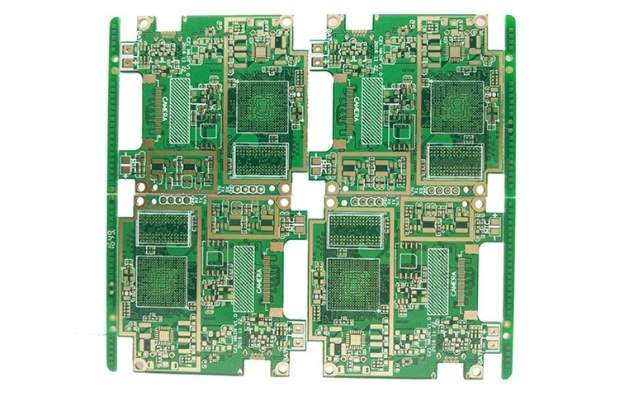
- Production Facility
- PCB Capabilities
- 6 layer PCB Stackup


| Feature | Capability |
| Quality Grade | Standard IPC 2 and IPC 3 |
| Number of Layers | 2 – 40layers |
| Order Quantity | 1pc – 1Million+pcs |
| Build Time | 24H – 4weeks |
| Material | S1150G, S1165, S1000-2 |
| Board Size | Min 5*5mm | Max 500*650mm |
| Board Thickness | 0.4mm – 6.5mm |
| Copper Weight (Finished) | 0.5oz – 10.0oz |
| Min Tracing/Spacing | 3mil/3mil |
| Solder Mask Sides | As per the file |
| Solder Mask Color | Green, White, Blue, Black, Red, Yellow |
| Silkscreen Sides | As per the file |
| Silkscreen Color | White, Black, Yellow |
| Surface Finish | HASL – Hot Air Solder Leveling |
| Lead-Free HASL – RoHS | |
| ENIG – Electroless Nickle/Immersion Gold – RoHS | |
| Immersion Silver – RoHS | |
| Immersion Tin – RoHS | |
| OSP – Organic Solderability Preservatives – RoHS | |
| Min Annular Ring | 4mil |
| Min Drilling Hole Diameter | 6mil |
| Other Techniques | Gold fingers |
| Blind/Buried Vias |
Please see the details of 6 layer PCB Stack-up as follows:


Releted Some Other PCBs


Why Choose SMTFAB for Your 6 Layer PCB
SMTFAB is a premier 6 layer PCB manufacturer for over 12 years in China. We are specialized in offering top-quality from PCB prototypes to large quantities orders. When you have urgent projects, please send them to us. We can provide 24H quick-turn service for you.
6 layer PCB means there are 6 layers to rout electrical signals: Signal Layer, Ground, Power, Ground, Signal layer, and Ground
We offer different types of 6 layer PCBs including a flexible circuit board, rigid-flex circuit board, Rogers + FR4 mixed PCB, HDI PCB, and so on.
In order to meet different demands for our customers, we have sufficient raw materials in stock, such as Shengyi, KB, Rogers, Nanya, Arlon, Nelco, Isola, and Bergquist.
We can also provide different colors of solder masks, including green, white, black, red, blue, orange, purple, and yellow.
SMTFAB has one expert engineering and production team, they can provide professional advice for your 6 layer printed circuit board project.
What’s more, SMTFAB can offer a turnkey solution for your project. From PCB design & layout, PCB fabrication to PCB assembly, all processes are in-house and not outsourcing.
We have passed many certifications like ISO9001, 14000, UL, REACH, and RoHS, so you can guarantee 100% production and reliable service for you.
If you are looking for a reputable 6 layer PCB supplier for your project and business, SMTFAB is your best choice.
SMTFAB has over 500 workers in our workshop and the monthly capacity is 40,000 square meters. We can meet your different demands from prototype to mass production.
Don’t hesitate to contact us when you have any questions.
6 Layer PCB | The Ultimate FAQ Guide
A Multilayer PCB contains a minimum of three layers of conductive materials. The layers adhere to one another via lamination.
6 Layer printed circuit boards (PCBs) are a kind of multilayer PCB. They provide many benefits over other kinds of PCBs. This kind of PCB is becoming more used in electrical devices. It makes the most of the power that electronics have to offer. We decided to address some of the concerns raised about the 6 Layer PCB.
- What Is 6 Layer PCB?
- What Are The Materials Of the 6 Layer PCB?
- Which Components Are Used In 6 Layer PCB?
- What Are 6 Layer PCB Applications?
- What Are The Advantages Of a 6 Layer PCB?
- What Is The Effect Of Loss Tangent Of 6 Layer PCB?
- How Does The Dielectric Constant Affect 6 Layer PCB?
- Why Do You Need To Consider The Temperature Change In A 6 Layer PCB?
- How Can You Ensure Impedance Control In 6 Layer PCB?
- Is 6 Layer PCB Moisture-Resistive?
- What Is The Coefficient Of Thermal Expansion In 6 Layer PCB?
- How Does The Glass Transition Temperature Affect 6 Layer PCB?
- 6 Layer PCB Better Than Single Layer PCB?
- What Are The Vias Used In 6 Layer PCB?
- What is the Most Used Copper Thickness In 6 Layer PCB?
- Can A 6 Layer PCB Be Customized?
- What Is The UL94 Rating Of 6 Layer PCB?
- How To Etch A 6 Layer PCB?
- What Are The Design Techniques Of 6 Layer PCB?
- Which Surface Finish Process Is Good For 6 Layer PCB?
- What Is The Manufacturing Process Of 6 Layer PCB?
- How Can You Test The Performance Of 6 Layer PCB?
- What Are The Limitations Of the 6 Layer PCB?
- How To Choose The Best Manufacturer Of 6 Layer PCB?
What Is 6 Layer PCB?
6 Layer PCBs are a kind of multilayer printed circuit board that contains six sheets of conductive material. It’s indeed primarily a four-layer PCB with two additional signal layers placed between the surfaces.
A standard six-layer PCB consists of the six layers listed below-
- Two exterior layers
- Two inner planes
- Two internal layers
In addition to providing superior routing for both high- and low-speed data, the architecture of the six-layer PCB reduces electromagnetic interference (EMI). To route high-speed communications, the two internal planes must be used in conjunction with the two surface layers.
A common 6 Layer PCB stack-up comprises the following layers:
- The most prominent layer
- Pre-Peg
- Ground plane
- Layer of routing
- Pre-peg
- The inner layer of the routing
- Core
- Plane of internal power
- Pre-peg
- Layer bottom

6 Layer PCB
What Are The Materials Of the 6 Layer PCB?
The material is selected based on the application, desired outcome, environmental considerations, and other PCB limitations. You should select the PCB material according to the anticipated outcomes. In 6 Layer PCB fabrication, these are the following materials that you can use:
FR-4
The Fr-4 is the most popular PCB material. It’s a glass-reinforced epoxy sheet, Water and flame-resistant epoxy is utilized. It is strong and light. This material’s tensile strength is exceptional.

FR4 PCB Material
Metal
PCBs are still constructed using conventional materials such as iron, copper, aluminum, and so on. These materials enable Surface Mount Technology (SMT) component insertion. They are also mechanically durable. Metal base PCBs have a significantly longer life span.
PTFE (Teflon)
In its most basic form, PTFE is a type of polymeric substance that offers no resistance, making it ideal for applications requiring high speed or frequency. Because PTFE is highly flexible, it is particularly useful in situations requiring tight tolerances. It is also quite light, making it suitable for many sectors. It is also flame-retardant, strong, heat-stable, and multi-purpose.
Which Components Are Used In 6 Layer PCB?
6 Layer PCBs are constructed of several electronic parts that are essential to the device they will be attached to. For a device to operate properly, the PCB must have elements like diodes, resistors, capacitors, and switches, working properly.

6 Layer PCB Components
Resistors
Resistors are a vital and typical element on a 6 Layer PCB. A current is sent through them to create a voltage, which is then dissipated as heat. To evaluate the resistance, they are available in a multitude of materials and colors.
Transistors
A transistor is essentially an amplifier that is used to change the electrical signals or regulate them. It has three pins: base, collector, and emitter.
Capacitors
After resistors, capacitors are the most often used element.
Transformers
Transformers are frequently used to raise or reduce the voltage of an electrical circuit.
Diodes
It is a circuit component that enables the current flow in one way. This can stop electricity flowing incorrectly, damaging the board and gadget. The most common diode is an LED, that emits light.
Sensors
The sensors detect changes in ambient conditions and generate an electrical message which is transmitted to other circuit board elements.
What Are 6 Layer PCB Applicationsations?
6 Layer PCBs are regarded to be the ideal option for a wide range of industrial applications because of their low weight as well as compact designs, according to industry experts. 6 Layer PCB applications are as follows:
Industrial Electronics
Consumer electronics and industrial electronics are quite different from one another. They undergo harsh circumstances like heat, stress, vibration, pressure, grit, and moisture. They are designed to function for a long time and can be constantly worked. Such circumstances are suitable for 6 Layer PCBs. Today, 6 Layer printed circuit boards outlive other market alternatives.
Medical Devices
In the medical sector, electronic gadgets are essential. The medical sector, like all other electronics-dependent industries, is miniaturizing.
The need for micro gadgets in the medical sector is increasing with non-invasive treatment methods gaining momentum. 6 Layer PCBs are ideal for these devices due to their compact size, low weight, and other strong characteristics.
MRI, X-ray, CT scan, blood pressure, IR temperature monitoring are some examples of medical equipment utilizing 6 Layer PCB.

Production Of 6 Layer PCB For Medical Equipment
Computers and Devices
We can no longer envision life without computers. Almost all computers and associated devices utilize 6 Layer PCBs due to the excellent space-saving and operational features. These PCBs may be developed to outperform other technologies while saving money.
Consumer Electronics
Consumer electronics include a broad variety of common electrical devices. Communication gadgets like smartphones and laptops, recreational devices like smart TVs and media players, and household appliances like microwaves and washing machines are examples of such products.
Most of these gadgets have a 6 Layer PCB, compared to conventional single-layer PCBs. Why? 6 Layer PCBs help them operate and be small.
Military, Aerospace, and Defense
Like the aforementioned sectors, the military and defense sectors are prioritizing 6 Layer circuit boards. Such PCBs are popular for their small size, lightweight, practicality, and durability.
Surveillance, aircraft defense systems, radar systems, and automated weapons use 6 Layer printed circuit boards. High-circuits need 6 Layer PCBs to resist severe environments where high temperatures and pressures may destroy the grade components.
Telecommunication Electronics
Many communications equipment, like GPS and satellite systems, use 6 Layer PCBs for communication systems, which requires both durability and functionality. With the growth of wireless communications, there is a strong need for high-performance small devices. 6 Layer circuit boards readily meet the need.
Other telecommunications electronics applications include power amplifiers, telecommunication towers, radar systems, and so many more.
What Are The Advantages Of a 6 Layer PCB?
In technological terms, 6 Layer PCBs provide many design benefits. You can get these advantages if you use 6 Layer PCB:
Small Size
A major and recognized advantage of utilizing 6 Layer PCBs is their size. Due to their layered architecture, they are naturally smaller with comparable performance than other PCBs.
This offers a significant advantage for contemporary electronics since the current tendency is towards smaller, more compact yet stronger devices such as smartphones, computers, tablets, and smartwatches.
High-Quality
Because of the amount of effort and preparation needed to build 6 Layer PCBs, these kinds of PCBs are more efficient in their quality over single and double-layer Circuit boards. As a consequence, they tend to be more stable.
Increased Durability
By their nature, 6 Layer PCBs are likely to be tough. Such 6 Layer printed circuit boards are not only capable of supporting their load, but also of dealing with the pressure and temperature required to bind them securely.
More Powerful
They are densely packed with several layers incorporated onto a single PCB. These narrow-end boards make them more connected and help them attain higher speed and reliability despite their reduced size.
Single Connection Point
They are intended to operate independently of other PCB elements. As a consequence, they just need one connecting point instead of numerous ones needed by several single-layer PCBs.
Because just one connecting point is required in the finished product, this also benefits electronic product designers. This is very useful for tiny devices and gadgets.
However, these features make 6 Layer PCBs ideal for mobile devices and high-performance electronics. Now that so many sectors are embracing mobile solutions, the 6 Layer PCBs are finding new possibilities.

6 Layer PCB Advantages
What Is The Effect Of Loss Tangent Of 6 Layer PCB?
In 6 Layer PCBs, the loss tangent is the measurement of the signal loss owing to the intrinsic electromagnetic heat transfer in the substratum of the PCB.
Loss tangent is essential for uses over 1 GHz and analog transmissions to calculate attenuation. The copper’s friction coefficient also raises losses. Loss tangent in PCB traces relies on frequencies, dielectric constant, and loss factor (Df). High-frequency losses have larger Dk and Df values.

6 Layer PCB Loss Factor
How Does The Dielectric Constant Affect 6 Layer PCB?
The imaginary component of the dielectric constant affects the speed of propagation of an electromagnetic wave through a substance. In 6 Layer PCB, signal propagation across a trace is determined by the dielectric constant as well as trace shape.
Why Do You Need To Consider The Temperature Change In A 6 Layer PCB?
Extreme temperature can affect the structure of your 6 Layer PCB, reducing its performance or even causing it to fail.
- Excess heat may harm your PCB in the following ways:
- Structural deterioration
- Circuit line disruption
- Incompatible material expansion rates
- Oxidation
How Can You Ensure Impedance Control In 6 Layer PCB?
You have to provide parameters for a few distinct factors to ensure the impedance control of your 6 Layer PCB:
- The impedance of the target
- Width of the trace
- Height of trace
- Impedance trace layer
- Copper element spacing on regulated traces

6 Layer PCB Impedance Control
If you have very specific requirements, you can try providing a chart with the specifications. Including a chart will help to clarify the ambiguity by visually displaying the data given.
Is 6 Layer PCB Moisture-Resistive?
Different functional defects on a PCB may lead to moisture, based on which elements or conducting routes come into touch with a diffusion. Humidity in the board may solidify the resin, glass surfaces or epoxy glass, and fractures.
Most films, however, regardless of thin or thick, offer sufficient protection from moisture if properly applied.
To make your 6 Layer PCB moisture resistant, watch this video.
What Is The Coefficient Of Thermal Expansion In 6 Layer PCB?
Thermal expansion coefficient (CTE) describes how much a 6 Layer PCB will stretch or shrink when subjected to heat or cold, respectively.
Depending on the material, the CTE will vary. Compared to epoxy resin which has a CTE rating of 30-40, copper has a CTE rating of 18. Because both materials inflate at different rates when heated, this CTE imbalance can cause issues throughout the PCB production process.
Boards are subjected to several heat cycles throughout the assembly process and throughout the PCB manufacturing operation, and this variation in the rate of expansion can lead to joint problems or damage.

Thermal Testing On PCB
How Does The Glass Transition Temperature Affect 6 Layer PCB?
“Tg” (glass transition temperature) is a physical characteristic that indicates when a glass changes from a hard, glassy state to one that is more flexible. Rather than melting, materials undergo structural reforms and become rubbery once the Tg is surpassed.
This is the temperature where fiberglass turns amorphous after lamination at extreme heat and under the stress of the various surface layers of a PCB.
This is not the peak working temperature of the PCB, but instead the heat which the PCB assembly can withstand for a short time until deterioration occurs.
Is 6 Layer PCB Better Than Single Layer PCB?
Single-layer PCB boards can’t compete with 6 Layer PCBs when it comes to overall performance and reliability. While smaller and lighter, 6- layer PCBs may achieve much with better EMI shielding, more controllable impedance characteristics, and better design integrity.
If you’re looking for a PCB for a small device, a 6 Layer PCB is the way to go.

Single Layer PCB vs 6 Layer PCB
What Are The Vias Used In 6 Layer PCB?
Blind via, buried via, and then through are the three most prevalent forms of PCB vias that you can apply to your 6 Layer PCB.
Plated through-hole (PTH)
The most frequent form of via is indeed the plated through-hole, which is a hole drilled through the many layers of a PCB. Along with being simple to use, it’s also quite cost-effective. You’ll lose some space on your PCB and can leave little room for the components, but it’ll be worth it.
Buried via
It’s a copper-plated hole between two or even more layers of circuit board that is not exposed from the outside. In addition, hidden vias in a PCB cannot be found since they are “buried” under the exterior layer interfaces of the PCB, which makes it impossible. Then there’s the fact that each buried via requires a separate drill file. PCBs with high density interconnects (HDI) often employ buried vias.
Blind via
A blind via is challenging to drill since it joins the bulk of the circuit’s outside with the insulating core located directly beneath it. The thickness of the hole is also important when making a blind passage.

Vias Used In 6 Layer PCB
What is the Most Used Copper Thickness In 6 Layer PCB?
When it comes to 6 Layer PCB circuit boards, the ideal manufacturing aspect is the conventional 6- layer PCB construction with 1/1/1/1/1/1 ounce thickness of copper.

6 Layer PCB Copper Thickness
Can A 6 Layer PCB Be Customized?
It is possible to design a 6 Layer PCB as per your needs. If you want, you can change the-
- Design
- Architecture
- Endurance
- Vias placing
- Holes
- Parts pacing and much more
What Is The UL94 Rating Of 6 Layer PCB?
Underwriters Laboratory (UL) conducts product testing, licenses manufacturers, and develops and maintains safety regulations for a variety of industrial applications.
The primary standards for PCBs are UL 796, which is a particular 6 Layer PCB standard, as well as UL 94, which is for flammability assessment of all plastics. These define the number of tests conducted that will be used to assess the 6 Layer PCB’s long-term dependability and flame safety.
When a board meets these requirements, it bears the UL logo, the circuit board type, and the maker’s logo. The UL94 rating of this PCB is V-0.

6 Layer PCB UL Rating
How To Etch A 6 Layer PCB?
Remove the undesired copper by dissolving (or etching away) the uncovered copper from the lining using a strongly alkaline solution.
The procedure is meticulously monitored to verify that the completed conductor widths match the specifications.
However, designers should keep in mind that bigger copper foils necessitate larger gaps between the lines. The operator double-checks that all of the undesirable copper has been removed.
Remove the blue photoresist that shielded the copper image afterward. So you’ve got the exact pattern that you need. The operator double-checks that all of the photo-resist is gone.

PCB Etching
For more information about etching, see this video.
What Are The Design Techniques Of 6 Layer PCB?
Here are a few helpful 6 Layer PCB design techniques:
- On the PCB, channel adjoining signal layers in opposing directions.
- Use layers for the power and ground planes.
- Decrease the effect of the through-hole pads on the innermost signal layer.

6 Layer PCB Design
Which Surface Finish Process Is Good For 6 Layer PCB?
Selecting the appropriate Surface Finish for your 6 Layer PCB is critical. If you choose the incorrect Surface Finish, you risk having problems with downstream assembly or long-term dependability.
These finishing processes are suitable for 6 Layer PCBs:
- Electroless Nickel/Immersion Gold (ENIG)
- Immersion Silver
- Hot Air Leveling (HAL)

PCB Surface Finish
What Is The Manufacturing Process Of 6 Layer PCB?
The stages in the 6 Layer PCB manufacturing process are as follows:
- On CAD, design a 6 Layer PCB.
- Make the inner layer core next.
- Prepreg and copper foil sheets are included in the lamination process.
- To keep the sheets aligned as they’re being stacked, holes are drilled into the sheets.
- The next stage is to use a preheated hydraulic press to generate force, heat, and vacuum.
- To create a six-layer PCB, prepreg resin is used to connect the layers, core, as well as foil.
How Can You Test The Performance Of 6 Layer PCB?
The following are the main tests for your 6 Layer PCB:
In-Circuit Test (ICT)
In-circuit testing (ICT) is indeed a PCB inspection technique that uses a bed of nails containing numerous probes.
Flying Probe
The flying probe testing process conducts tests with two to six needles that glide or fly across the board.

PCB Flying Probe Test
CableScan
The CableScan program is a good choice for evaluating PCBs with many connections, such as backplanes and other complicated interface boards.
CableScan connects to the circuit to be examined through connectors and checks each pin against any other pin for manufacturing issues such as soldering shorts or openings. It will also check the jumper arrangement and diode functioning, as well as analyze resistance and inductance.
Functional Test
The most thorough test to establish your board’s ultimate pass/fail result is to do functional testing. The functional test setup will mimic the board’s actions based on your requirements using a mix of connected connections, test probes, as well as evaluation of the programs.
What Are The Limitations Of the 6 Layer PCB?
6 Layer PCB boards, despite their benefits, have certain drawbacks. As a result, you should examine them as well.
- More Expensive
- Production Is Complex
- High-skilled workers are required.
- Time to Produce
How To Choose The Best Manufacturer Of 6 Layer PCB?
Finding a reliable 6 Layer PCB maker isn’t always simple. However, if you want to save effort and time by skipping the lengthy track, consider the following factor-
- Your board design
- How they’re dealing with Thermal Relief from
- Make certain they’re utilizing the appropriate materials.
- What they’re doing with the parts and how they’re putting them together
- The cost of the service
- Your PCB manufacturing timeframe
- The PCB shipment method
Conclusion
The 6 Layer PCB gives you additional options and possibilities in the areas where you want to use it. The 6 Layer PCB is small, lightweight, inexpensive, and performs well.
We hope that this FAQ guide has given you a better understanding of the 6 Layer PCB. SMTFAB is the leading 6 Layer PCB supplier in China. Please feel free to contact us if you have any queries about 6 Layer PCB. All of your questions will be answered by our specialist.
Your Premier 6 Layer PCB Manufacturer in China
As one reliable 6 layer PCB supplier in China, we can provide one-stop solution for your project.
- Over 12 years 6 layer PCB manufacturing experience
- Offer a free sample before your mass production order
- 100% E-test and AOI inspection
- Provide WIP(work in process) report to you each week
- 48h quick-turn service for your prototype 6 layer PCB
- Follow up your local working time and quote in time
- Production Facility
- PCB Capabilities
- 6 layer PCB Stackup
| Feature | Capability |
| Quality Grade | Standard IPC 2 and IPC 3 |
| Number of Layers | 2 – 40layers |
| Order Quantity | 1pc – 1Million+pcs |
| Build Time | 24H – 4weeks |
| Material | S1150G, S1165, S1000-2 |
| Board Size | Min 5*5mm | Max 500*650mm |
| Board Thickness | 0.4mm – 6.5mm |
| Copper Weight (Finished) | 0.5oz – 10.0oz |
| Min Tracing/Spacing | 3mil/3mil |
| Solder Mask Sides | As per the file |
| Solder Mask Color | Green, White, Blue, Black, Red, Yellow |
| Silkscreen Sides | As per the file |
| Silkscreen Color | White, Black, Yellow |
| Surface Finish | HASL – Hot Air Solder Leveling |
| Lead-Free HASL – RoHS | |
| ENIG – Electroless Nickle/Immersion Gold – RoHS | |
| Immersion Silver – RoHS | |
| Immersion Tin – RoHS | |
| OSP – Organic Solderability Preservatives – RoHS | |
| Min Annular Ring | 4mil |
| Min Drilling Hole Diameter | 6mil |
| Other Techniques | Gold fingers |
| Blind/Buried Vias |
Please see the details of 6 layer PCB Stack-up as follows:
Releted Some Other PCBs
Why Choose SMTFAB for Your 6 Layer PCB
SMTFAB is a premier 6 layer PCB manufacturer for over 12 years in China. We are specialized in offering top-quality from PCB prototypes to large quantities orders. When you have urgent projects, please send them to us. We can provide 24H quick-turn service for you.
6 layer PCB means there are 6 layers to rout electrical signals: Signal Layer, Ground, Power, Ground, Signal layer, and Ground
We offer different types of 6 layer PCBs including a flexible circuit board, rigid-flex circuit board, Rogers + FR4 mixed PCB, HDI PCB, and so on.
In order to meet different demands for our customers, we have sufficient raw materials in stock, such as Shengyi, KB, Rogers, Nanya, Arlon, Nelco, Isola, and Bergquist.
We can also provide different colors of solder masks, including green, white, black, red, blue, orange, purple, and yellow.
SMTFAB has one expert engineering and production team, they can provide professional advice for your 6 layer printed circuit board project.
What’s more, SMTFAB can offer a turnkey solution for your project. From PCB design & layout, PCB fabrication to PCB assembly, all processes are in-house and not outsourcing.
We have passed many certifications like ISO9001, 14000, UL, REACH, and RoHS, so you can guarantee 100% production and reliable service for you.
If you are looking for a reputable 6 layer PCB supplier for your project and business, SMTFAB is your best choice.
SMTFAB has over 500 workers in our workshop and the monthly capacity is 40,000 square meters. We can meet your different demands from prototype to mass production.
Don’t hesitate to contact us when you have any questions.
6 Layer PCB | The Ultimate FAQ Guide
A Multilayer PCB contains a minimum of three layers of conductive materials. The layers adhere to one another via lamination.
6 Layer printed circuit boards (PCBs) are a kind of multilayer PCB. They provide many benefits over other kinds of PCBs. This kind of PCB is becoming more used in electrical devices. It makes the most of the power that electronics have to offer. We decided to address some of the concerns raised about the 6 Layer PCB.
- What Is 6 Layer PCB?
- What Are The Materials Of the 6 Layer PCB?
- Which Components Are Used In 6 Layer PCB?
- What Are 6 Layer PCB Applications?
- What Are The Advantages Of a 6 Layer PCB?
- What Is The Effect Of Loss Tangent Of 6 Layer PCB?
- How Does The Dielectric Constant Affect 6 Layer PCB?
- Why Do You Need To Consider The Temperature Change In A 6 Layer PCB?
- How Can You Ensure Impedance Control In 6 Layer PCB?
- Is 6 Layer PCB Moisture-Resistive?
- What Is The Coefficient Of Thermal Expansion In 6 Layer PCB?
- How Does The Glass Transition Temperature Affect 6 Layer PCB?
- 6 Layer PCB Better Than Single Layer PCB?
- What Are The Vias Used In 6 Layer PCB?
- What is the Most Used Copper Thickness In 6 Layer PCB?
- Can A 6 Layer PCB Be Customized?
- What Is The UL94 Rating Of 6 Layer PCB?
- How To Etch A 6 Layer PCB?
- What Are The Design Techniques Of 6 Layer PCB?
- Which Surface Finish Process Is Good For 6 Layer PCB?
- What Is The Manufacturing Process Of 6 Layer PCB?
- How Can You Test The Performance Of 6 Layer PCB?
- What Are The Limitations Of the 6 Layer PCB?
- How To Choose The Best Manufacturer Of 6 Layer PCB?
What Is 6 Layer PCB?
6 Layer PCBs are a kind of multilayer printed circuit board that contains six sheets of conductive material. It’s indeed primarily a four-layer PCB with two additional signal layers placed between the surfaces.
A standard six-layer PCB consists of the six layers listed below-
- Two exterior layers
- Two inner planes
- Two internal layers
In addition to providing superior routing for both high- and low-speed data, the architecture of the six-layer PCB reduces electromagnetic interference (EMI). To route high-speed communications, the two internal planes must be used in conjunction with the two surface layers.
A common 6 Layer PCB stack-up comprises the following layers:
- The most prominent layer
- Pre-Peg
- Ground plane
- Layer of routing
- Pre-peg
- The inner layer of the routing
- Core
- Plane of internal power
- Pre-peg
- Layer bottom
6 Layer PCB
What Are The Materials Of the 6 Layer PCB?
The material is selected based on the application, desired outcome, environmental considerations, and other PCB limitations. You should select the PCB material according to the anticipated outcomes. In 6 Layer PCB fabrication, these are the following materials that you can use:
FR-4
The Fr-4 is the most popular PCB material. It’s a glass-reinforced epoxy sheet, Water and flame-resistant epoxy is utilized. It is strong and light. This material’s tensile strength is exceptional.
FR4 PCB Material
Metal
PCBs are still constructed using conventional materials such as iron, copper, aluminum, and so on. These materials enable Surface Mount Technology (SMT) component insertion. They are also mechanically durable. Metal base PCBs have a significantly longer life span.
PTFE (Teflon)
In its most basic form, PTFE is a type of polymeric substance that offers no resistance, making it ideal for applications requiring high speed or frequency. Because PTFE is highly flexible, it is particularly useful in situations requiring tight tolerances. It is also quite light, making it suitable for many sectors. It is also flame-retardant, strong, heat-stable, and multi-purpose.
Which Components Are Used In 6 Layer PCB?
6 Layer PCBs are constructed of several electronic parts that are essential to the device they will be attached to. For a device to operate properly, the PCB must have elements like diodes, resistors, capacitors, and switches, working properly.
6 Layer PCB Components
Resistors
Resistors are a vital and typical element on a 6 Layer PCB. A current is sent through them to create a voltage, which is then dissipated as heat. To evaluate the resistance, they are available in a multitude of materials and colors.
Transistors
A transistor is essentially an amplifier that is used to change the electrical signals or regulate them. It has three pins: base, collector, and emitter.
Capacitors
After resistors, capacitors are the most often used element.
Transformers
Transformers are frequently used to raise or reduce the voltage of an electrical circuit.
Diodes
It is a circuit component that enables the current flow in one way. This can stop electricity flowing incorrectly, damaging the board and gadget. The most common diode is an LED, that emits light.
Sensors
The sensors detect changes in ambient conditions and generate an electrical message which is transmitted to other circuit board elements.
What Are 6 Layer PCB Applicationsations?
6 Layer PCBs are regarded to be the ideal option for a wide range of industrial applications because of their low weight as well as compact designs, according to industry experts. 6 Layer PCB applications are as follows:
Industrial Electronics
Consumer electronics and industrial electronics are quite different from one another. They undergo harsh circumstances like heat, stress, vibration, pressure, grit, and moisture. They are designed to function for a long time and can be constantly worked. Such circumstances are suitable for 6 Layer PCBs. Today, 6 Layer printed circuit boards outlive other market alternatives.
Medical Devices
In the medical sector, electronic gadgets are essential. The medical sector, like all other electronics-dependent industries, is miniaturizing.
The need for micro gadgets in the medical sector is increasing with non-invasive treatment methods gaining momentum. 6 Layer PCBs are ideal for these devices due to their compact size, low weight, and other strong characteristics.
MRI, X-ray, CT scan, blood pressure, IR temperature monitoring are some examples of medical equipment utilizing 6 Layer PCB.
Production Of 6 Layer PCB For Medical Equipment
Computers and Devices
We can no longer envision life without computers. Almost all computers and associated devices utilize 6 Layer PCBs due to the excellent space-saving and operational features. These PCBs may be developed to outperform other technologies while saving money.
Consumer Electronics
Consumer electronics include a broad variety of common electrical devices. Communication gadgets like smartphones and laptops, recreational devices like smart TVs and media players, and household appliances like microwaves and washing machines are examples of such products.
Most of these gadgets have a 6 Layer PCB, compared to conventional single-layer PCBs. Why? 6 Layer PCBs help them operate and be small.
Military, Aerospace, and Defense
Like the aforementioned sectors, the military and defense sectors are prioritizing 6 Layer circuit boards. Such PCBs are popular for their small size, lightweight, practicality, and durability.
Surveillance, aircraft defense systems, radar systems, and automated weapons use 6 Layer printed circuit boards. High-circuits need 6 Layer PCBs to resist severe environments where high temperatures and pressures may destroy the grade components.
Telecommunication Electronics
Many communications equipment, like GPS and satellite systems, use 6 Layer PCBs for communication systems, which requires both durability and functionality. With the growth of wireless communications, there is a strong need for high-performance small devices. 6 Layer circuit boards readily meet the need.
Other telecommunications electronics applications include power amplifiers, telecommunication towers, radar systems, and so many more.
What Are The Advantages Of a 6 Layer PCB?
In technological terms, 6 Layer PCBs provide many design benefits. You can get these advantages if you use 6 Layer PCB:
Small Size
A major and recognized advantage of utilizing 6 Layer PCBs is their size. Due to their layered architecture, they are naturally smaller with comparable performance than other PCBs.
This offers a significant advantage for contemporary electronics since the current tendency is towards smaller, more compact yet stronger devices such as smartphones, computers, tablets, and smartwatches.
High-Quality
Because of the amount of effort and preparation needed to build 6 Layer PCBs, these kinds of PCBs are more efficient in their quality over single and double-layer Circuit boards. As a consequence, they tend to be more stable.
Increased Durability
By their nature, 6 Layer PCBs are likely to be tough. Such 6 Layer printed circuit boards are not only capable of supporting their load, but also of dealing with the pressure and temperature required to bind them securely.
More Powerful
They are densely packed with several layers incorporated onto a single PCB. These narrow-end boards make them more connected and help them attain higher speed and reliability despite their reduced size.
Single Connection Point
They are intended to operate independently of other PCB elements. As a consequence, they just need one connecting point instead of numerous ones needed by several single-layer PCBs.
Because just one connecting point is required in the finished product, this also benefits electronic product designers. This is very useful for tiny devices and gadgets.
However, these features make 6 Layer PCBs ideal for mobile devices and high-performance electronics. Now that so many sectors are embracing mobile solutions, the 6 Layer PCBs are finding new possibilities.
6 Layer PCB Advantages
What Is The Effect Of Loss Tangent Of 6 Layer PCB?
In 6 Layer PCBs, the loss tangent is the measurement of the signal loss owing to the intrinsic electromagnetic heat transfer in the substratum of the PCB.
Loss tangent is essential for uses over 1 GHz and analog transmissions to calculate attenuation. The copper’s friction coefficient also raises losses. Loss tangent in PCB traces relies on frequencies, dielectric constant, and loss factor (Df). High-frequency losses have larger Dk and Df values.
6 Layer PCB Loss Factor
How Does The Dielectric Constant Affect 6 Layer PCB?
The imaginary component of the dielectric constant affects the speed of propagation of an electromagnetic wave through a substance. In 6 Layer PCB, signal propagation across a trace is determined by the dielectric constant as well as trace shape.
Why Do You Need To Consider The Temperature Change In A 6 Layer PCB?
Extreme temperature can affect the structure of your 6 Layer PCB, reducing its performance or even causing it to fail.
- Excess heat may harm your PCB in the following ways:
- Structural deterioration
- Circuit line disruption
- Incompatible material expansion rates
- Oxidation
How Can You Ensure Impedance Control In 6 Layer PCB?
You have to provide parameters for a few distinct factors to ensure the impedance control of your 6 Layer PCB:
- The impedance of the target
- Width of the trace
- Height of trace
- Impedance trace layer
- Copper element spacing on regulated traces
6 Layer PCB Impedance Control
If you have very specific requirements, you can try providing a chart with the specifications. Including a chart will help to clarify the ambiguity by visually displaying the data given.
Is 6 Layer PCB Moisture-Resistive?
Different functional defects on a PCB may lead to moisture, based on which elements or conducting routes come into touch with a diffusion. Humidity in the board may solidify the resin, glass surfaces or epoxy glass, and fractures.
Most films, however, regardless of thin or thick, offer sufficient protection from moisture if properly applied.
To make your 6 Layer PCB moisture resistant, watch this video.
What Is The Coefficient Of Thermal Expansion In 6 Layer PCB?
Thermal expansion coefficient (CTE) describes how much a 6 Layer PCB will stretch or shrink when subjected to heat or cold, respectively.
Depending on the material, the CTE will vary. Compared to epoxy resin which has a CTE rating of 30-40, copper has a CTE rating of 18. Because both materials inflate at different rates when heated, this CTE imbalance can cause issues throughout the PCB production process.
Boards are subjected to several heat cycles throughout the assembly process and throughout the PCB manufacturing operation, and this variation in the rate of expansion can lead to joint problems or damage.
Thermal Testing On PCB
How Does The Glass Transition Temperature Affect 6 Layer PCB?
“Tg” (glass transition temperature) is a physical characteristic that indicates when a glass changes from a hard, glassy state to one that is more flexible. Rather than melting, materials undergo structural reforms and become rubbery once the Tg is surpassed.
This is the temperature where fiberglass turns amorphous after lamination at extreme heat and under the stress of the various surface layers of a PCB.
This is not the peak working temperature of the PCB, but instead the heat which the PCB assembly can withstand for a short time until deterioration occurs.
Is 6 Layer PCB Better Than Single Layer PCB?
Single-layer PCB boards can’t compete with 6 Layer PCBs when it comes to overall performance and reliability. While smaller and lighter, 6- layer PCBs may achieve much with better EMI shielding, more controllable impedance characteristics, and better design integrity.
If you’re looking for a PCB for a small device, a 6 Layer PCB is the way to go.
Single Layer PCB vs 6 Layer PCB
What Are The Vias Used In 6 Layer PCB?
Blind via, buried via, and then through are the three most prevalent forms of PCB vias that you can apply to your 6 Layer PCB.
Plated through-hole (PTH)
The most frequent form of via is indeed the plated through-hole, which is a hole drilled through the many layers of a PCB. Along with being simple to use, it’s also quite cost-effective. You’ll lose some space on your PCB and can leave little room for the components, but it’ll be worth it.
Buried via
It’s a copper-plated hole between two or even more layers of circuit board that is not exposed from the outside. In addition, hidden vias in a PCB cannot be found since they are “buried” under the exterior layer interfaces of the PCB, which makes it impossible. Then there’s the fact that each buried via requires a separate drill file. PCBs with high density interconnects (HDI) often employ buried vias.
Blind via
A blind via is challenging to drill since it joins the bulk of the circuit’s outside with the insulating core located directly beneath it. The thickness of the hole is also important when making a blind passage.
Vias Used In 6 Layer PCB
What is the Most Used Copper Thickness In 6 Layer PCB?
When it comes to 6 Layer PCB circuit boards, the ideal manufacturing aspect is the conventional 6- layer PCB construction with 1/1/1/1/1/1 ounce thickness of copper.
6 Layer PCB Copper Thickness
Can A 6 Layer PCB Be Customized?
It is possible to design a 6 Layer PCB as per your needs. If you want, you can change the-
- Design
- Architecture
- Endurance
- Vias placing
- Holes
- Parts pacing and much more
What Is The UL94 Rating Of 6 Layer PCB?
Underwriters Laboratory (UL) conducts product testing, licenses manufacturers, and develops and maintains safety regulations for a variety of industrial applications.
The primary standards for PCBs are UL 796, which is a particular 6 Layer PCB standard, as well as UL 94, which is for flammability assessment of all plastics. These define the number of tests conducted that will be used to assess the 6 Layer PCB’s long-term dependability and flame safety.
When a board meets these requirements, it bears the UL logo, the circuit board type, and the maker’s logo. The UL94 rating of this PCB is V-0.
6 Layer PCB UL Rating
How To Etch A 6 Layer PCB?
Remove the undesired copper by dissolving (or etching away) the uncovered copper from the lining using a strongly alkaline solution.
The procedure is meticulously monitored to verify that the completed conductor widths match the specifications.
However, designers should keep in mind that bigger copper foils necessitate larger gaps between the lines. The operator double-checks that all of the undesirable copper has been removed.
Remove the blue photoresist that shielded the copper image afterward. So you’ve got the exact pattern that you need. The operator double-checks that all of the photo-resist is gone.
PCB Etching
For more information about etching, see this video.
What Are The Design Techniques Of 6 Layer PCB?
Here are a few helpful 6 Layer PCB design techniques:
- On the PCB, channel adjoining signal layers in opposing directions.
- Use layers for the power and ground planes.
- Decrease the effect of the through-hole pads on the innermost signal layer.
6 Layer PCB Design
Which Surface Finish Process Is Good For 6 Layer PCB?
Selecting the appropriate Surface Finish for your 6 Layer PCB is critical. If you choose the incorrect Surface Finish, you risk having problems with downstream assembly or long-term dependability.
These finishing processes are suitable for 6 Layer PCBs:
- Electroless Nickel/Immersion Gold (ENIG)
- Immersion Silver
- Hot Air Leveling (HAL)
PCB Surface Finish
What Is The Manufacturing Process Of 6 Layer PCB?
The stages in the 6 Layer PCB manufacturing process are as follows:
- On CAD, design a 6 Layer PCB.
- Make the inner layer core next.
- Prepreg and copper foil sheets are included in the lamination process.
- To keep the sheets aligned as they’re being stacked, holes are drilled into the sheets.
- The next stage is to use a preheated hydraulic press to generate force, heat, and vacuum.
- To create a six-layer PCB, prepreg resin is used to connect the layers, core, as well as foil.
How Can You Test The Performance Of 6 Layer PCB?
The following are the main tests for your 6 Layer PCB:
In-Circuit Test (ICT)
In-circuit testing (ICT) is indeed a PCB inspection technique that uses a bed of nails containing numerous probes.
Flying Probe
The flying probe testing process conducts tests with two to six needles that glide or fly across the board.
PCB Flying Probe Test
CableScan
The CableScan program is a good choice for evaluating PCBs with many connections, such as backplanes and other complicated interface boards.
CableScan connects to the circuit to be examined through connectors and checks each pin against any other pin for manufacturing issues such as soldering shorts or openings. It will also check the jumper arrangement and diode functioning, as well as analyze resistance and inductance.
Functional Test
The most thorough test to establish your board’s ultimate pass/fail result is to do functional testing. The functional test setup will mimic the board’s actions based on your requirements using a mix of connected connections, test probes, as well as evaluation of the programs.
What Are The Limitations Of the 6 Layer PCB?
6 Layer PCB boards, despite their benefits, have certain drawbacks. As a result, you should examine them as well.
- More Expensive
- Production Is Complex
- High-skilled workers are required.
- Time to Produce
How To Choose The Best Manufacturer Of 6 Layer PCB?
Finding a reliable 6 Layer PCB maker isn’t always simple. However, if you want to save effort and time by skipping the lengthy track, consider the following factor-
- Your board design
- How they’re dealing with Thermal Relief from
- Make certain they’re utilizing the appropriate materials.
- What they’re doing with the parts and how they’re putting them together
- The cost of the service
- Your PCB manufacturing timeframe
- The PCB shipment method
Conclusion
The 6 Layer PCB gives you additional options and possibilities in the areas where you want to use it. The 6 Layer PCB is small, lightweight, inexpensive, and performs well.
We hope that this FAQ guide has given you a better understanding of the 6 Layer PCB. SMTFAB is the leading 6 Layer PCB supplier in China. Please feel free to contact us if you have any queries about 6 Layer PCB. All of your questions will be answered by our specialist.
Your Premier 6 Layer PCB Manufacturer in China
As one reliable 6 layer PCB supplier in China, we can provide one-stop solution for your project.
- Over 12 years 6 layer PCB manufacturing experience
- Offer a free sample before your mass production order
- 100% E-test and AOI inspection
- Provide WIP(work in process) report to you each week
- 48h quick-turn service for your prototype 6 layer PCB
- Follow up your local working time and quote in time
Your Premier 6 Layer PCB Manufacturer in China
Your Premier 6 Layer PCB Manufacturer in China
As one reliable 6 layer PCB supplier in China, we can provide one-stop solution for your project.
- Over 12 years 6 layer PCB manufacturing experience
- Offer a free sample before your mass production order
- 100% E-test and AOI inspection
- Provide WIP(work in process) report to you each week
- 48h quick-turn service for your prototype 6 layer PCB
- Follow up your local working time and quote in time
- Production Facility
- PCB Capabilities
- 6 layer PCB Stackup
| Feature | Capability |
| Quality Grade | Standard IPC 2 and IPC 3 |
| Number of Layers | 2 – 40layers |
| Order Quantity | 1pc – 1Million+pcs |
| Build Time | 24H – 4weeks |
| Material | S1150G, S1165, S1000-2 |
| Board Size | Min 5*5mm | Max 500*650mm |
| Board Thickness | 0.4mm – 6.5mm |
| Copper Weight (Finished) | 0.5oz – 10.0oz |
| Min Tracing/Spacing | 3mil/3mil |
| Solder Mask Sides | As per the file |
| Solder Mask Color | Green, White, Blue, Black, Red, Yellow |
| Silkscreen Sides | As per the file |
| Silkscreen Color | White, Black, Yellow |
| Surface Finish | HASL – Hot Air Solder Leveling |
| Lead-Free HASL – RoHS | |
| ENIG – Electroless Nickle/Immersion Gold – RoHS | |
| Immersion Silver – RoHS | |
| Immersion Tin – RoHS | |
| OSP – Organic Solderability Preservatives – RoHS | |
| Min Annular Ring | 4mil |
| Min Drilling Hole Diameter | 6mil |
| Other Techniques | Gold fingers |
| Blind/Buried Vias |
Please see the details of 6 layer PCB Stack-up as follows:
- Production Facility
- PCB Capabilities
- 6 layer PCB Stackup
| Feature | Capability |
| Quality Grade | Standard IPC 2 and IPC 3 |
| Number of Layers | 2 – 40layers |
| Order Quantity | 1pc – 1Million+pcs |
| Build Time | 24H – 4weeks |
| Material | S1150G, S1165, S1000-2 |
| Board Size | Min 5*5mm | Max 500*650mm |
| Board Thickness | 0.4mm – 6.5mm |
| Copper Weight (Finished) | 0.5oz – 10.0oz |
| Min Tracing/Spacing | 3mil/3mil |
| Solder Mask Sides | As per the file |
| Solder Mask Color | Green, White, Blue, Black, Red, Yellow |
| Silkscreen Sides | As per the file |
| Silkscreen Color | White, Black, Yellow |
| Surface Finish | HASL – Hot Air Solder Leveling |
| Lead-Free HASL – RoHS | |
| ENIG – Electroless Nickle/Immersion Gold – RoHS | |
| Immersion Silver – RoHS | |
| Immersion Tin – RoHS | |
| OSP – Organic Solderability Preservatives – RoHS | |
| Min Annular Ring | 4mil |
| Min Drilling Hole Diameter | 6mil |
| Other Techniques | Gold fingers |
| Blind/Buried Vias |
Please see the details of 6 layer PCB Stack-up as follows:
Please see the details of 6 layer PCB Stack-up as follows:
Releted Some Other PCBs
Releted Some Other PCBs
Why Choose SMTFAB for Your 6 Layer PCB
SMTFAB is a premier 6 layer PCB manufacturer for over 12 years in China. We are specialized in offering top-quality from PCB prototypes to large quantities orders. When you have urgent projects, please send them to us. We can provide 24H quick-turn service for you.
6 layer PCB means there are 6 layers to rout electrical signals: Signal Layer, Ground, Power, Ground, Signal layer, and Ground
We offer different types of 6 layer PCBs including a flexible circuit board, rigid-flex circuit board, Rogers + FR4 mixed PCB, HDI PCB, and so on.
In order to meet different demands for our customers, we have sufficient raw materials in stock, such as Shengyi, KB, Rogers, Nanya, Arlon, Nelco, Isola, and Bergquist.
We can also provide different colors of solder masks, including green, white, black, red, blue, orange, purple, and yellow.
SMTFAB has one expert engineering and production team, they can provide professional advice for your 6 layer printed circuit board project.
What’s more, SMTFAB can offer a turnkey solution for your project. From PCB design & layout, PCB fabrication to PCB assembly, all processes are in-house and not outsourcing.
We have passed many certifications like ISO9001, 14000, UL, REACH, and RoHS, so you can guarantee 100% production and reliable service for you.
If you are looking for a reputable 6 layer PCB supplier for your project and business, SMTFAB is your best choice.
SMTFAB has over 500 workers in our workshop and the monthly capacity is 40,000 square meters. We can meet your different demands from prototype to mass production.
Don’t hesitate to contact us when you have any questions.
6 Layer PCB | The Ultimate FAQ Guide
A Multilayer PCB contains a minimum of three layers of conductive materials. The layers adhere to one another via lamination.
6 Layer printed circuit boards (PCBs) are a kind of multilayer PCB. They provide many benefits over other kinds of PCBs. This kind of PCB is becoming more used in electrical devices. It makes the most of the power that electronics have to offer. We decided to address some of the concerns raised about the 6 Layer PCB.
- What Is 6 Layer PCB?
- What Are The Materials Of the 6 Layer PCB?
- Which Components Are Used In 6 Layer PCB?
- What Are 6 Layer PCB Applications?
- What Are The Advantages Of a 6 Layer PCB?
- What Is The Effect Of Loss Tangent Of 6 Layer PCB?
- How Does The Dielectric Constant Affect 6 Layer PCB?
- Why Do You Need To Consider The Temperature Change In A 6 Layer PCB?
- How Can You Ensure Impedance Control In 6 Layer PCB?
- Is 6 Layer PCB Moisture-Resistive?
- What Is The Coefficient Of Thermal Expansion In 6 Layer PCB?
- How Does The Glass Transition Temperature Affect 6 Layer PCB?
- 6 Layer PCB Better Than Single Layer PCB?
- What Are The Vias Used In 6 Layer PCB?
- What is the Most Used Copper Thickness In 6 Layer PCB?
- Can A 6 Layer PCB Be Customized?
- What Is The UL94 Rating Of 6 Layer PCB?
- How To Etch A 6 Layer PCB?
- What Are The Design Techniques Of 6 Layer PCB?
- Which Surface Finish Process Is Good For 6 Layer PCB?
- What Is The Manufacturing Process Of 6 Layer PCB?
- How Can You Test The Performance Of 6 Layer PCB?
- What Are The Limitations Of the 6 Layer PCB?
- How To Choose The Best Manufacturer Of 6 Layer PCB?
What Is 6 Layer PCB?
6 Layer PCBs are a kind of multilayer printed circuit board that contains six sheets of conductive material. It’s indeed primarily a four-layer PCB with two additional signal layers placed between the surfaces.
A standard six-layer PCB consists of the six layers listed below-
- Two exterior layers
- Two inner planes
- Two internal layers
In addition to providing superior routing for both high- and low-speed data, the architecture of the six-layer PCB reduces electromagnetic interference (EMI). To route high-speed communications, the two internal planes must be used in conjunction with the two surface layers.
A common 6 Layer PCB stack-up comprises the following layers:
- The most prominent layer
- Pre-Peg
- Ground plane
- Layer of routing
- Pre-peg
- The inner layer of the routing
- Core
- Plane of internal power
- Pre-peg
- Layer bottom
6 Layer PCB
What Are The Materials Of the 6 Layer PCB?
The material is selected based on the application, desired outcome, environmental considerations, and other PCB limitations. You should select the PCB material according to the anticipated outcomes. In 6 Layer PCB fabrication, these are the following materials that you can use:
FR-4
The Fr-4 is the most popular PCB material. It’s a glass-reinforced epoxy sheet, Water and flame-resistant epoxy is utilized. It is strong and light. This material’s tensile strength is exceptional.
FR4 PCB Material
Metal
PCBs are still constructed using conventional materials such as iron, copper, aluminum, and so on. These materials enable Surface Mount Technology (SMT) component insertion. They are also mechanically durable. Metal base PCBs have a significantly longer life span.
PTFE (Teflon)
In its most basic form, PTFE is a type of polymeric substance that offers no resistance, making it ideal for applications requiring high speed or frequency. Because PTFE is highly flexible, it is particularly useful in situations requiring tight tolerances. It is also quite light, making it suitable for many sectors. It is also flame-retardant, strong, heat-stable, and multi-purpose.
Which Components Are Used In 6 Layer PCB?
6 Layer PCBs are constructed of several electronic parts that are essential to the device they will be attached to. For a device to operate properly, the PCB must have elements like diodes, resistors, capacitors, and switches, working properly.
6 Layer PCB Components
Resistors
Resistors are a vital and typical element on a 6 Layer PCB. A current is sent through them to create a voltage, which is then dissipated as heat. To evaluate the resistance, they are available in a multitude of materials and colors.
Transistors
A transistor is essentially an amplifier that is used to change the electrical signals or regulate them. It has three pins: base, collector, and emitter.
Capacitors
After resistors, capacitors are the most often used element.
Transformers
Transformers are frequently used to raise or reduce the voltage of an electrical circuit.
Diodes
It is a circuit component that enables the current flow in one way. This can stop electricity flowing incorrectly, damaging the board and gadget. The most common diode is an LED, that emits light.
Sensors
The sensors detect changes in ambient conditions and generate an electrical message which is transmitted to other circuit board elements.
What Are 6 Layer PCB Applicationsations?
6 Layer PCBs are regarded to be the ideal option for a wide range of industrial applications because of their low weight as well as compact designs, according to industry experts. 6 Layer PCB applications are as follows:
Industrial Electronics
Consumer electronics and industrial electronics are quite different from one another. They undergo harsh circumstances like heat, stress, vibration, pressure, grit, and moisture. They are designed to function for a long time and can be constantly worked. Such circumstances are suitable for 6 Layer PCBs. Today, 6 Layer printed circuit boards outlive other market alternatives.
Medical Devices
In the medical sector, electronic gadgets are essential. The medical sector, like all other electronics-dependent industries, is miniaturizing.
The need for micro gadgets in the medical sector is increasing with non-invasive treatment methods gaining momentum. 6 Layer PCBs are ideal for these devices due to their compact size, low weight, and other strong characteristics.
MRI, X-ray, CT scan, blood pressure, IR temperature monitoring are some examples of medical equipment utilizing 6 Layer PCB.
Production Of 6 Layer PCB For Medical Equipment
Computers and Devices
We can no longer envision life without computers. Almost all computers and associated devices utilize 6 Layer PCBs due to the excellent space-saving and operational features. These PCBs may be developed to outperform other technologies while saving money.
Consumer Electronics
Consumer electronics include a broad variety of common electrical devices. Communication gadgets like smartphones and laptops, recreational devices like smart TVs and media players, and household appliances like microwaves and washing machines are examples of such products.
Most of these gadgets have a 6 Layer PCB, compared to conventional single-layer PCBs. Why? 6 Layer PCBs help them operate and be small.
Military, Aerospace, and Defense
Like the aforementioned sectors, the military and defense sectors are prioritizing 6 Layer circuit boards. Such PCBs are popular for their small size, lightweight, practicality, and durability.
Surveillance, aircraft defense systems, radar systems, and automated weapons use 6 Layer printed circuit boards. High-circuits need 6 Layer PCBs to resist severe environments where high temperatures and pressures may destroy the grade components.
Telecommunication Electronics
Many communications equipment, like GPS and satellite systems, use 6 Layer PCBs for communication systems, which requires both durability and functionality. With the growth of wireless communications, there is a strong need for high-performance small devices. 6 Layer circuit boards readily meet the need.
Other telecommunications electronics applications include power amplifiers, telecommunication towers, radar systems, and so many more.
What Are The Advantages Of a 6 Layer PCB?
In technological terms, 6 Layer PCBs provide many design benefits. You can get these advantages if you use 6 Layer PCB:
Small Size
A major and recognized advantage of utilizing 6 Layer PCBs is their size. Due to their layered architecture, they are naturally smaller with comparable performance than other PCBs.
This offers a significant advantage for contemporary electronics since the current tendency is towards smaller, more compact yet stronger devices such as smartphones, computers, tablets, and smartwatches.
High-Quality
Because of the amount of effort and preparation needed to build 6 Layer PCBs, these kinds of PCBs are more efficient in their quality over single and double-layer Circuit boards. As a consequence, they tend to be more stable.
Increased Durability
By their nature, 6 Layer PCBs are likely to be tough. Such 6 Layer printed circuit boards are not only capable of supporting their load, but also of dealing with the pressure and temperature required to bind them securely.
More Powerful
They are densely packed with several layers incorporated onto a single PCB. These narrow-end boards make them more connected and help them attain higher speed and reliability despite their reduced size.
Single Connection Point
They are intended to operate independently of other PCB elements. As a consequence, they just need one connecting point instead of numerous ones needed by several single-layer PCBs.
Because just one connecting point is required in the finished product, this also benefits electronic product designers. This is very useful for tiny devices and gadgets.
However, these features make 6 Layer PCBs ideal for mobile devices and high-performance electronics. Now that so many sectors are embracing mobile solutions, the 6 Layer PCBs are finding new possibilities.
6 Layer PCB Advantages
What Is The Effect Of Loss Tangent Of 6 Layer PCB?
In 6 Layer PCBs, the loss tangent is the measurement of the signal loss owing to the intrinsic electromagnetic heat transfer in the substratum of the PCB.
Loss tangent is essential for uses over 1 GHz and analog transmissions to calculate attenuation. The copper’s friction coefficient also raises losses. Loss tangent in PCB traces relies on frequencies, dielectric constant, and loss factor (Df). High-frequency losses have larger Dk and Df values.
6 Layer PCB Loss Factor
How Does The Dielectric Constant Affect 6 Layer PCB?
The imaginary component of the dielectric constant affects the speed of propagation of an electromagnetic wave through a substance. In 6 Layer PCB, signal propagation across a trace is determined by the dielectric constant as well as trace shape.
Why Do You Need To Consider The Temperature Change In A 6 Layer PCB?
Extreme temperature can affect the structure of your 6 Layer PCB, reducing its performance or even causing it to fail.
- Excess heat may harm your PCB in the following ways:
- Structural deterioration
- Circuit line disruption
- Incompatible material expansion rates
- Oxidation
How Can You Ensure Impedance Control In 6 Layer PCB?
You have to provide parameters for a few distinct factors to ensure the impedance control of your 6 Layer PCB:
- The impedance of the target
- Width of the trace
- Height of trace
- Impedance trace layer
- Copper element spacing on regulated traces
6 Layer PCB Impedance Control
If you have very specific requirements, you can try providing a chart with the specifications. Including a chart will help to clarify the ambiguity by visually displaying the data given.
Is 6 Layer PCB Moisture-Resistive?
Different functional defects on a PCB may lead to moisture, based on which elements or conducting routes come into touch with a diffusion. Humidity in the board may solidify the resin, glass surfaces or epoxy glass, and fractures.
Most films, however, regardless of thin or thick, offer sufficient protection from moisture if properly applied.
To make your 6 Layer PCB moisture resistant, watch this video.
What Is The Coefficient Of Thermal Expansion In 6 Layer PCB?
Thermal expansion coefficient (CTE) describes how much a 6 Layer PCB will stretch or shrink when subjected to heat or cold, respectively.
Depending on the material, the CTE will vary. Compared to epoxy resin which has a CTE rating of 30-40, copper has a CTE rating of 18. Because both materials inflate at different rates when heated, this CTE imbalance can cause issues throughout the PCB production process.
Boards are subjected to several heat cycles throughout the assembly process and throughout the PCB manufacturing operation, and this variation in the rate of expansion can lead to joint problems or damage.
Thermal Testing On PCB
How Does The Glass Transition Temperature Affect 6 Layer PCB?
“Tg” (glass transition temperature) is a physical characteristic that indicates when a glass changes from a hard, glassy state to one that is more flexible. Rather than melting, materials undergo structural reforms and become rubbery once the Tg is surpassed.
This is the temperature where fiberglass turns amorphous after lamination at extreme heat and under the stress of the various surface layers of a PCB.
This is not the peak working temperature of the PCB, but instead the heat which the PCB assembly can withstand for a short time until deterioration occurs.
Is 6 Layer PCB Better Than Single Layer PCB?
Single-layer PCB boards can’t compete with 6 Layer PCBs when it comes to overall performance and reliability. While smaller and lighter, 6- layer PCBs may achieve much with better EMI shielding, more controllable impedance characteristics, and better design integrity.
If you’re looking for a PCB for a small device, a 6 Layer PCB is the way to go.
Single Layer PCB vs 6 Layer PCB
What Are The Vias Used In 6 Layer PCB?
Blind via, buried via, and then through are the three most prevalent forms of PCB vias that you can apply to your 6 Layer PCB.
Plated through-hole (PTH)
The most frequent form of via is indeed the plated through-hole, which is a hole drilled through the many layers of a PCB. Along with being simple to use, it’s also quite cost-effective. You’ll lose some space on your PCB and can leave little room for the components, but it’ll be worth it.
Buried via
It’s a copper-plated hole between two or even more layers of circuit board that is not exposed from the outside. In addition, hidden vias in a PCB cannot be found since they are “buried” under the exterior layer interfaces of the PCB, which makes it impossible. Then there’s the fact that each buried via requires a separate drill file. PCBs with high density interconnects (HDI) often employ buried vias.
Blind via
A blind via is challenging to drill since it joins the bulk of the circuit’s outside with the insulating core located directly beneath it. The thickness of the hole is also important when making a blind passage.
Vias Used In 6 Layer PCB
What is the Most Used Copper Thickness In 6 Layer PCB?
When it comes to 6 Layer PCB circuit boards, the ideal manufacturing aspect is the conventional 6- layer PCB construction with 1/1/1/1/1/1 ounce thickness of copper.
6 Layer PCB Copper Thickness
Can A 6 Layer PCB Be Customized?
It is possible to design a 6 Layer PCB as per your needs. If you want, you can change the-
- Design
- Architecture
- Endurance
- Vias placing
- Holes
- Parts pacing and much more
What Is The UL94 Rating Of 6 Layer PCB?
Underwriters Laboratory (UL) conducts product testing, licenses manufacturers, and develops and maintains safety regulations for a variety of industrial applications.
The primary standards for PCBs are UL 796, which is a particular 6 Layer PCB standard, as well as UL 94, which is for flammability assessment of all plastics. These define the number of tests conducted that will be used to assess the 6 Layer PCB’s long-term dependability and flame safety.
When a board meets these requirements, it bears the UL logo, the circuit board type, and the maker’s logo. The UL94 rating of this PCB is V-0.
6 Layer PCB UL Rating
How To Etch A 6 Layer PCB?
Remove the undesired copper by dissolving (or etching away) the uncovered copper from the lining using a strongly alkaline solution.
The procedure is meticulously monitored to verify that the completed conductor widths match the specifications.
However, designers should keep in mind that bigger copper foils necessitate larger gaps between the lines. The operator double-checks that all of the undesirable copper has been removed.
Remove the blue photoresist that shielded the copper image afterward. So you’ve got the exact pattern that you need. The operator double-checks that all of the photo-resist is gone.
PCB Etching
For more information about etching, see this video.
What Are The Design Techniques Of 6 Layer PCB?
Here are a few helpful 6 Layer PCB design techniques:
- On the PCB, channel adjoining signal layers in opposing directions.
- Use layers for the power and ground planes.
- Decrease the effect of the through-hole pads on the innermost signal layer.
6 Layer PCB Design
Which Surface Finish Process Is Good For 6 Layer PCB?
Selecting the appropriate Surface Finish for your 6 Layer PCB is critical. If you choose the incorrect Surface Finish, you risk having problems with downstream assembly or long-term dependability.
These finishing processes are suitable for 6 Layer PCBs:
- Electroless Nickel/Immersion Gold (ENIG)
- Immersion Silver
- Hot Air Leveling (HAL)
PCB Surface Finish
What Is The Manufacturing Process Of 6 Layer PCB?
The stages in the 6 Layer PCB manufacturing process are as follows:
- On CAD, design a 6 Layer PCB.
- Make the inner layer core next.
- Prepreg and copper foil sheets are included in the lamination process.
- To keep the sheets aligned as they’re being stacked, holes are drilled into the sheets.
- The next stage is to use a preheated hydraulic press to generate force, heat, and vacuum.
- To create a six-layer PCB, prepreg resin is used to connect the layers, core, as well as foil.
How Can You Test The Performance Of 6 Layer PCB?
The following are the main tests for your 6 Layer PCB:
In-Circuit Test (ICT)
In-circuit testing (ICT) is indeed a PCB inspection technique that uses a bed of nails containing numerous probes.
Flying Probe
The flying probe testing process conducts tests with two to six needles that glide or fly across the board.
PCB Flying Probe Test
CableScan
The CableScan program is a good choice for evaluating PCBs with many connections, such as backplanes and other complicated interface boards.
CableScan connects to the circuit to be examined through connectors and checks each pin against any other pin for manufacturing issues such as soldering shorts or openings. It will also check the jumper arrangement and diode functioning, as well as analyze resistance and inductance.
Functional Test
The most thorough test to establish your board’s ultimate pass/fail result is to do functional testing. The functional test setup will mimic the board’s actions based on your requirements using a mix of connected connections, test probes, as well as evaluation of the programs.
What Are The Limitations Of the 6 Layer PCB?
6 Layer PCB boards, despite their benefits, have certain drawbacks. As a result, you should examine them as well.
- More Expensive
- Production Is Complex
- High-skilled workers are required.
- Time to Produce
How To Choose The Best Manufacturer Of 6 Layer PCB?
Finding a reliable 6 Layer PCB maker isn’t always simple. However, if you want to save effort and time by skipping the lengthy track, consider the following factor-
- Your board design
- How they’re dealing with Thermal Relief from
- Make certain they’re utilizing the appropriate materials.
- What they’re doing with the parts and how they’re putting them together
- The cost of the service
- Your PCB manufacturing timeframe
- The PCB shipment method
Conclusion
The 6 Layer PCB gives you additional options and possibilities in the areas where you want to use it. The 6 Layer PCB is small, lightweight, inexpensive, and performs well.
We hope that this FAQ guide has given you a better understanding of the 6 Layer PCB. SMTFAB is the leading 6 Layer PCB supplier in China. Please feel free to contact us if you have any queries about 6 Layer PCB. All of your questions will be answered by our specialist.
Why Choose SMTFAB for Your 6 Layer PCB
SMTFAB is a premier 6 layer PCB manufacturer for over 12 years in China. We are specialized in offering top-quality from PCB prototypes to large quantities orders. When you have urgent projects, please send them to us. We can provide 24H quick-turn service for you.
6 layer PCB means there are 6 layers to rout electrical signals: Signal Layer, Ground, Power, Ground, Signal layer, and Ground
We offer different types of 6 layer PCBs including a flexible circuit board, rigid-flex circuit board, Rogers + FR4 mixed PCB, HDI PCB, and so on.
In order to meet different demands for our customers, we have sufficient raw materials in stock, such as Shengyi, KB, Rogers, Nanya, Arlon, Nelco, Isola, and Bergquist.
We can also provide different colors of solder masks, including green, white, black, red, blue, orange, purple, and yellow.
SMTFAB has one expert engineering and production team, they can provide professional advice for your 6 layer printed circuit board project.
What’s more, SMTFAB can offer a turnkey solution for your project. From PCB design & layout, PCB fabrication to PCB assembly, all processes are in-house and not outsourcing.
We have passed many certifications like ISO9001, 14000, UL, REACH, and RoHS, so you can guarantee 100% production and reliable service for you.
If you are looking for a reputable 6 layer PCB supplier for your project and business, SMTFAB is your best choice.
SMTFAB has over 500 workers in our workshop and the monthly capacity is 40,000 square meters. We can meet your different demands from prototype to mass production.
Don’t hesitate to contact us when you have any questions.
6 Layer PCB | The Ultimate FAQ Guide
A Multilayer PCB contains a minimum of three layers of conductive materials. The layers adhere to one another via lamination.
6 Layer printed circuit boards (PCBs) are a kind of multilayer PCB. They provide many benefits over other kinds of PCBs. This kind of PCB is becoming more used in electrical devices. It makes the most of the power that electronics have to offer. We decided to address some of the concerns raised about the 6 Layer PCB.
- What Is 6 Layer PCB?
- What Are The Materials Of the 6 Layer PCB?
- Which Components Are Used In 6 Layer PCB?
- What Are 6 Layer PCB Applications?
- What Are The Advantages Of a 6 Layer PCB?
- What Is The Effect Of Loss Tangent Of 6 Layer PCB?
- How Does The Dielectric Constant Affect 6 Layer PCB?
- Why Do You Need To Consider The Temperature Change In A 6 Layer PCB?
- How Can You Ensure Impedance Control In 6 Layer PCB?
- Is 6 Layer PCB Moisture-Resistive?
- What Is The Coefficient Of Thermal Expansion In 6 Layer PCB?
- How Does The Glass Transition Temperature Affect 6 Layer PCB?
- 6 Layer PCB Better Than Single Layer PCB?
- What Are The Vias Used In 6 Layer PCB?
- What is the Most Used Copper Thickness In 6 Layer PCB?
- Can A 6 Layer PCB Be Customized?
- What Is The UL94 Rating Of 6 Layer PCB?
- How To Etch A 6 Layer PCB?
- What Are The Design Techniques Of 6 Layer PCB?
- Which Surface Finish Process Is Good For 6 Layer PCB?
- What Is The Manufacturing Process Of 6 Layer PCB?
- How Can You Test The Performance Of 6 Layer PCB?
- What Are The Limitations Of the 6 Layer PCB?
- How To Choose The Best Manufacturer Of 6 Layer PCB?
6 Layer PCBs are a kind of multilayer printed circuit board that contains six sheets of conductive material. It’s indeed primarily a four-layer PCB with two additional signal layers placed between the surfaces.
A standard six-layer PCB consists of the six layers listed below-
- Two exterior layers
- Two inner planes
- Two internal layers
In addition to providing superior routing for both high- and low-speed data, the architecture of the six-layer PCB reduces electromagnetic interference (EMI). To route high-speed communications, the two internal planes must be used in conjunction with the two surface layers.
A common 6 Layer PCB stack-up comprises the following layers:
- The most prominent layer
- Pre-Peg
- Ground plane
- Layer of routing
- Pre-peg
- The inner layer of the routing
- Core
- Plane of internal power
- Pre-peg
- Layer bottom
What Are The Materials Of the 6 Layer PCB?
The material is selected based on the application, desired outcome, environmental considerations, and other PCB limitations. You should select the PCB material according to the anticipated outcomes. In 6 Layer PCB fabrication, these are the following materials that you can use:
The Fr-4 is the most popular PCB material. It’s a glass-reinforced epoxy sheet, Water and flame-resistant epoxy is utilized. It is strong and light. This material’s tensile strength is exceptional.
PCBs are still constructed using conventional materials such as iron, copper, aluminum, and so on. These materials enable Surface Mount Technology (SMT) component insertion. They are also mechanically durable. Metal base PCBs have a significantly longer life span.
In its most basic form, PTFE is a type of polymeric substance that offers no resistance, making it ideal for applications requiring high speed or frequency. Because PTFE is highly flexible, it is particularly useful in situations requiring tight tolerances. It is also quite light, making it suitable for many sectors. It is also flame-retardant, strong, heat-stable, and multi-purpose.
Which Components Are Used In 6 Layer PCB?
6 Layer PCBs are constructed of several electronic parts that are essential to the device they will be attached to. For a device to operate properly, the PCB must have elements like diodes, resistors, capacitors, and switches, working properly.
6 Layer PCB Components
Resistors are a vital and typical element on a 6 Layer PCB. A current is sent through them to create a voltage, which is then dissipated as heat. To evaluate the resistance, they are available in a multitude of materials and colors.
A transistor is essentially an amplifier that is used to change the electrical signals or regulate them. It has three pins: base, collector, and emitter.
After resistors, capacitors are the most often used element.
Transformers are frequently used to raise or reduce the voltage of an electrical circuit.
It is a circuit component that enables the current flow in one way. This can stop electricity flowing incorrectly, damaging the board and gadget. The most common diode is an LED, that emits light.
The sensors detect changes in ambient conditions and generate an electrical message which is transmitted to other circuit board elements.
What Are 6 Layer PCB Applicationsations?
6 Layer PCBs are regarded to be the ideal option for a wide range of industrial applications because of their low weight as well as compact designs, according to industry experts. 6 Layer PCB applications are as follows:
Industrial Electronics
Consumer electronics and industrial electronics are quite different from one another. They undergo harsh circumstances like heat, stress, vibration, pressure, grit, and moisture. They are designed to function for a long time and can be constantly worked. Such circumstances are suitable for 6 Layer PCBs. Today, 6 Layer printed circuit boards outlive other market alternatives.
In the medical sector, electronic gadgets are essential. The medical sector, like all other electronics-dependent industries, is miniaturizing.
The need for micro gadgets in the medical sector is increasing with non-invasive treatment methods gaining momentum. 6 Layer PCBs are ideal for these devices due to their compact size, low weight, and other strong characteristics.
MRI, X-ray, CT scan, blood pressure, IR temperature monitoring are some examples of medical equipment utilizing 6 Layer PCB.
Production Of 6 Layer PCB For Medical Equipment
Computers and Devices
We can no longer envision life without computers. Almost all computers and associated devices utilize 6 Layer PCBs due to the excellent space-saving and operational features. These PCBs may be developed to outperform other technologies while saving money.
Consumer electronics include a broad variety of common electrical devices. Communication gadgets like smartphones and laptops, recreational devices like smart TVs and media players, and household appliances like microwaves and washing machines are examples of such products.
Most of these gadgets have a 6 Layer PCB, compared to conventional single-layer PCBs. Why? 6 Layer PCBs help them operate and be small.
Military, Aerospace, and Defense
Like the aforementioned sectors, the military and defense sectors are prioritizing 6 Layer circuit boards. Such PCBs are popular for their small size, lightweight, practicality, and durability.
Surveillance, aircraft defense systems, radar systems, and automated weapons use 6 Layer printed circuit boards. High-circuits need 6 Layer PCBs to resist severe environments where high temperatures and pressures may destroy the grade components.
Telecommunication Electronics
Many communications equipment, like GPS and satellite systems, use 6 Layer PCBs for communication systems, which requires both durability and functionality. With the growth of wireless communications, there is a strong need for high-performance small devices. 6 Layer circuit boards readily meet the need.
Other telecommunications electronics applications include power amplifiers, telecommunication towers, radar systems, and so many more.
What Are The Advantages Of a 6 Layer PCB?
In technological terms, 6 Layer PCBs provide many design benefits. You can get these advantages if you use 6 Layer PCB:
A major and recognized advantage of utilizing 6 Layer PCBs is their size. Due to their layered architecture, they are naturally smaller with comparable performance than other PCBs.
This offers a significant advantage for contemporary electronics since the current tendency is towards smaller, more compact yet stronger devices such as smartphones, computers, tablets, and smartwatches.
Because of the amount of effort and preparation needed to build 6 Layer PCBs, these kinds of PCBs are more efficient in their quality over single and double-layer Circuit boards. As a consequence, they tend to be more stable.
By their nature, 6 Layer PCBs are likely to be tough. Such 6 Layer printed circuit boards are not only capable of supporting their load, but also of dealing with the pressure and temperature required to bind them securely.
They are densely packed with several layers incorporated onto a single PCB. These narrow-end boards make them more connected and help them attain higher speed and reliability despite their reduced size.
Single Connection Point
They are intended to operate independently of other PCB elements. As a consequence, they just need one connecting point instead of numerous ones needed by several single-layer PCBs.
Because just one connecting point is required in the finished product, this also benefits electronic product designers. This is very useful for tiny devices and gadgets.
However, these features make 6 Layer PCBs ideal for mobile devices and high-performance electronics. Now that so many sectors are embracing mobile solutions, the 6 Layer PCBs are finding new possibilities.
6 Layer PCB Advantages
What Is The Effect Of Loss Tangent Of 6 Layer PCB?
In 6 Layer PCBs, the loss tangent is the measurement of the signal loss owing to the intrinsic electromagnetic heat transfer in the substratum of the PCB.
Loss tangent is essential for uses over 1 GHz and analog transmissions to calculate attenuation. The copper’s friction coefficient also raises losses. Loss tangent in PCB traces relies on frequencies, dielectric constant, and loss factor (Df). High-frequency losses have larger Dk and Df values.
6 Layer PCB Loss Factor
How Does The Dielectric Constant Affect 6 Layer PCB?
The imaginary component of the dielectric constant affects the speed of propagation of an electromagnetic wave through a substance. In 6 Layer PCB, signal propagation across a trace is determined by the dielectric constant as well as trace shape.
Why Do You Need To Consider The Temperature Change In A 6 Layer PCB?
Extreme temperature can affect the structure of your 6 Layer PCB, reducing its performance or even causing it to fail.
- Excess heat may harm your PCB in the following ways:
- Structural deterioration
- Circuit line disruption
- Incompatible material expansion rates
- Oxidation
How Can You Ensure Impedance Control In 6 Layer PCB?
You have to provide parameters for a few distinct factors to ensure the impedance control of your 6 Layer PCB:
- The impedance of the target
- Width of the trace
- Height of trace
- Impedance trace layer
- Copper element spacing on regulated traces
6 Layer PCB Impedance Control
If you have very specific requirements, you can try providing a chart with the specifications. Including a chart will help to clarify the ambiguity by visually displaying the data given.
Is 6 Layer PCB Moisture-Resistive?
Different functional defects on a PCB may lead to moisture, based on which elements or conducting routes come into touch with a diffusion. Humidity in the board may solidify the resin, glass surfaces or epoxy glass, and fractures.
Most films, however, regardless of thin or thick, offer sufficient protection from moisture if properly applied.
To make your 6 Layer PCB moisture resistant, watch this video.
What Is The Coefficient Of Thermal Expansion In 6 Layer PCB?
Thermal expansion coefficient (CTE) describes how much a 6 Layer PCB will stretch or shrink when subjected to heat or cold, respectively.
Depending on the material, the CTE will vary. Compared to epoxy resin which has a CTE rating of 30-40, copper has a CTE rating of 18. Because both materials inflate at different rates when heated, this CTE imbalance can cause issues throughout the PCB production process.
Boards are subjected to several heat cycles throughout the assembly process and throughout the PCB manufacturing operation, and this variation in the rate of expansion can lead to joint problems or damage.
Thermal Testing On PCB
How Does The Glass Transition Temperature Affect 6 Layer PCB?
“Tg” (glass transition temperature) is a physical characteristic that indicates when a glass changes from a hard, glassy state to one that is more flexible. Rather than melting, materials undergo structural reforms and become rubbery once the Tg is surpassed.
This is the temperature where fiberglass turns amorphous after lamination at extreme heat and under the stress of the various surface layers of a PCB.
This is not the peak working temperature of the PCB, but instead the heat which the PCB assembly can withstand for a short time until deterioration occurs.
Is 6 Layer PCB Better Than Single Layer PCB?
Single-layer PCB boards can’t compete with 6 Layer PCBs when it comes to overall performance and reliability. While smaller and lighter, 6- layer PCBs may achieve much with better EMI shielding, more controllable impedance characteristics, and better design integrity.
If you’re looking for a PCB for a small device, a 6 Layer PCB is the way to go.
Single Layer PCB vs 6 Layer PCB
What Are The Vias Used In 6 Layer PCB?
Blind via, buried via, and then through are the three most prevalent forms of PCB vias that you can apply to your 6 Layer PCB.
Plated through-hole (PTH)
The most frequent form of via is indeed the plated through-hole, which is a hole drilled through the many layers of a PCB. Along with being simple to use, it’s also quite cost-effective. You’ll lose some space on your PCB and can leave little room for the components, but it’ll be worth it.
It’s a copper-plated hole between two or even more layers of circuit board that is not exposed from the outside. In addition, hidden vias in a PCB cannot be found since they are “buried” under the exterior layer interfaces of the PCB, which makes it impossible. Then there’s the fact that each buried via requires a separate drill file. PCBs with high density interconnects (HDI) often employ buried vias.
A blind via is challenging to drill since it joins the bulk of the circuit’s outside with the insulating core located directly beneath it. The thickness of the hole is also important when making a blind passage.
Vias Used In 6 Layer PCB
What is the Most Used Copper Thickness In 6 Layer PCB?
When it comes to 6 Layer PCB circuit boards, the ideal manufacturing aspect is the conventional 6- layer PCB construction with 1/1/1/1/1/1 ounce thickness of copper.
6 Layer PCB Copper Thickness
Can A 6 Layer PCB Be Customized?
It is possible to design a 6 Layer PCB as per your needs. If you want, you can change the-
- Design
- Architecture
- Endurance
- Vias placing
- Holes
- Parts pacing and much more
What Is The UL94 Rating Of 6 Layer PCB?
Underwriters Laboratory (UL) conducts product testing, licenses manufacturers, and develops and maintains safety regulations for a variety of industrial applications.
The primary standards for PCBs are UL 796, which is a particular 6 Layer PCB standard, as well as UL 94, which is for flammability assessment of all plastics. These define the number of tests conducted that will be used to assess the 6 Layer PCB’s long-term dependability and flame safety.
When a board meets these requirements, it bears the UL logo, the circuit board type, and the maker’s logo. The UL94 rating of this PCB is V-0.
6 Layer PCB UL Rating
How To Etch A 6 Layer PCB?
Remove the undesired copper by dissolving (or etching away) the uncovered copper from the lining using a strongly alkaline solution.
The procedure is meticulously monitored to verify that the completed conductor widths match the specifications.
However, designers should keep in mind that bigger copper foils necessitate larger gaps between the lines. The operator double-checks that all of the undesirable copper has been removed.
Remove the blue photoresist that shielded the copper image afterward. So you’ve got the exact pattern that you need. The operator double-checks that all of the photo-resist is gone.
For more information about etching, see this video.
What Are The Design Techniques Of 6 Layer PCB?
Here are a few helpful 6 Layer PCB design techniques:
- On the PCB, channel adjoining signal layers in opposing directions.
- Use layers for the power and ground planes.
- Decrease the effect of the through-hole pads on the innermost signal layer.
Which Surface Finish Process Is Good For 6 Layer PCB?
Selecting the appropriate Surface Finish for your 6 Layer PCB is critical. If you choose the incorrect Surface Finish, you risk having problems with downstream assembly or long-term dependability.
These finishing processes are suitable for 6 Layer PCBs:
- Electroless Nickel/Immersion Gold (ENIG)
- Immersion Silver
- Hot Air Leveling (HAL)
What Is The Manufacturing Process Of 6 Layer PCB?
The stages in the 6 Layer PCB manufacturing process are as follows:
- On CAD, design a 6 Layer PCB.
- Make the inner layer core next.
- Prepreg and copper foil sheets are included in the lamination process.
- To keep the sheets aligned as they’re being stacked, holes are drilled into the sheets.
- The next stage is to use a preheated hydraulic press to generate force, heat, and vacuum.
- To create a six-layer PCB, prepreg resin is used to connect the layers, core, as well as foil.
How Can You Test The Performance Of 6 Layer PCB?
The following are the main tests for your 6 Layer PCB:
In-Circuit Test (ICT)
In-circuit testing (ICT) is indeed a PCB inspection technique that uses a bed of nails containing numerous probes.
The flying probe testing process conducts tests with two to six needles that glide or fly across the board.
PCB Flying Probe Test
The CableScan program is a good choice for evaluating PCBs with many connections, such as backplanes and other complicated interface boards.
CableScan connects to the circuit to be examined through connectors and checks each pin against any other pin for manufacturing issues such as soldering shorts or openings. It will also check the jumper arrangement and diode functioning, as well as analyze resistance and inductance.
The most thorough test to establish your board’s ultimate pass/fail result is to do functional testing. The functional test setup will mimic the board’s actions based on your requirements using a mix of connected connections, test probes, as well as evaluation of the programs.
What Are The Limitations Of the 6 Layer PCB?
6 Layer PCB boards, despite their benefits, have certain drawbacks. As a result, you should examine them as well.
- More Expensive
- Production Is Complex
- High-skilled workers are required.
- Time to Produce
How To Choose The Best Manufacturer Of 6 Layer PCB?
Finding a reliable 6 Layer PCB maker isn’t always simple. However, if you want to save effort and time by skipping the lengthy track, consider the following factor-
- Your board design
- How they’re dealing with Thermal Relief from
- Make certain they’re utilizing the appropriate materials.
- What they’re doing with the parts and how they’re putting them together
- The cost of the service
- Your PCB manufacturing timeframe
- The PCB shipment method
The 6 Layer PCB gives you additional options and possibilities in the areas where you want to use it. The 6 Layer PCB is small, lightweight, inexpensive, and performs well.
We hope that this FAQ guide has given you a better understanding of the 6 Layer PCB. SMTFAB is the leading 6 Layer PCB supplier in China. Please feel free to contact us if you have any queries about 6 Layer PCB. All of your questions will be answered by our specialist.
Technical Specifications
| 0 | { |
| 1 | " |
| 2 | F |
| 3 | e |
| 4 | a |
| 5 | t |
| 6 | u |
| 7 | r |
| 8 | e |
| 9 | " |
| 10 | : |
| 11 | " |
| 12 | C |
| 13 | a |
| 14 | p |
| 15 | a |
| 16 | b |
| 17 | i |
| 18 | l |
| 19 | i |
| 20 | t |
| 21 | y |
| 22 | " |
| 23 | , |
| 24 | " |
| 25 | Q |
| 26 | u |
| 27 | a |
| 28 | l |
| 29 | i |
| 30 | t |
| 31 | y |
| 32 | |
| 33 | G |
| 34 | r |
| 35 | a |
| 36 | d |
| 37 | e |
| 38 | " |
| 39 | : |
| 40 | " |
| 41 | S |
| 42 | t |
| 43 | a |
| 44 | n |
| 45 | d |
| 46 | a |
| 47 | r |
| 48 | d |
| 49 | |
| 50 | I |
| 51 | P |
| 52 | C |
| 53 | |
| 54 | 2 |
| 55 | |
| 56 | a |
| 57 | n |
| 58 | d |
| 59 | |
| 60 | I |
| 61 | P |
| 62 | C |
| 63 | |
| 64 | 3 |
| 65 | " |
| 66 | , |
| 67 | " |
| 68 | N |
| 69 | u |
| 70 | m |
| 71 | b |
| 72 | e |
| 73 | r |
| 74 | |
| 75 | o |
| 76 | f |
| 77 | |
| 78 | L |
| 79 | a |
| 80 | y |
| 81 | e |
| 82 | r |
| 83 | s |
| 84 | " |
| 85 | : |
| 86 | " |
| 87 | 2 |
| 88 | |
| 89 | – |
| 90 | |
| 91 | 4 |
| 92 | 0 |
| 93 | l |
| 94 | a |
| 95 | y |
| 96 | e |
| 97 | r |
| 98 | s |
| 99 | " |
| 100 | , |
| 101 | " |
| 102 | O |
| 103 | r |
| 104 | d |
| 105 | e |
| 106 | r |
| 107 | |
| 108 | Q |
| 109 | u |
| 110 | a |
| 111 | n |
| 112 | t |
| 113 | i |
| 114 | t |
| 115 | y |
| 116 | " |
| 117 | : |
| 118 | " |
| 119 | 1 |
| 120 | p |
| 121 | c |
| 122 | |
| 123 | – |
| 124 | |
| 125 | 1 |
| 126 | M |
| 127 | i |
| 128 | l |
| 129 | l |
| 130 | i |
| 131 | o |
| 132 | n |
| 133 | + |
| 134 | p |
| 135 | c |
| 136 | s |
| 137 | " |
| 138 | , |
| 139 | " |
| 140 | B |
| 141 | u |
| 142 | i |
| 143 | l |
| 144 | d |
| 145 | |
| 146 | T |
| 147 | i |
| 148 | m |
| 149 | e |
| 150 | " |
| 151 | : |
| 152 | " |
| 153 | 2 |
| 154 | 4 |
| 155 | H |
| 156 | |
| 157 | – |
| 158 | |
| 159 | 4 |
| 160 | w |
| 161 | e |
| 162 | e |
| 163 | k |
| 164 | s |
| 165 | " |
| 166 | , |
| 167 | " |
| 168 | M |
| 169 | a |
| 170 | t |
| 171 | e |
| 172 | r |
| 173 | i |
| 174 | a |
| 175 | l |
| 176 | " |
| 177 | : |
| 178 | " |
| 179 | S |
| 180 | 1 |
| 181 | 1 |
| 182 | 5 |
| 183 | 0 |
| 184 | G |
| 185 | , |
| 186 | |
| 187 | S |
| 188 | 1 |
| 189 | 1 |
| 190 | 6 |
| 191 | 5 |
| 192 | , |
| 193 | |
| 194 | S |
| 195 | 1 |
| 196 | 0 |
| 197 | 0 |
| 198 | 0 |
| 199 | - |
| 200 | 2 |
| 201 | " |
| 202 | , |
| 203 | " |
| 204 | B |
| 205 | o |
| 206 | a |
| 207 | r |
| 208 | d |
| 209 | |
| 210 | S |
| 211 | i |
| 212 | z |
| 213 | e |
| 214 | " |
| 215 | : |
| 216 | " |
| 217 | M |
| 218 | i |
| 219 | n |
| 220 | |
| 221 | 5 |
| 222 | * |
| 223 | 5 |
| 224 | m |
| 225 | m |
| 226 | |
| 227 | | |
| 228 | |
| 229 | M |
| 230 | a |
| 231 | x |
| 232 | |
| 233 | 5 |
| 234 | 0 |
| 235 | 0 |
| 236 | * |
| 237 | 6 |
| 238 | 5 |
| 239 | 0 |
| 240 | m |
| 241 | m |
| 242 | " |
| 243 | , |
| 244 | " |
| 245 | B |
| 246 | o |
| 247 | a |
| 248 | r |
| 249 | d |
| 250 | |
| 251 | T |
| 252 | h |
| 253 | i |
| 254 | c |
| 255 | k |
| 256 | n |
| 257 | e |
| 258 | s |
| 259 | s |
| 260 | " |
| 261 | : |
| 262 | " |
| 263 | 0 |
| 264 | . |
| 265 | 4 |
| 266 | m |
| 267 | m |
| 268 | |
| 269 | – |
| 270 | |
| 271 | 6 |
| 272 | . |
| 273 | 5 |
| 274 | m |
| 275 | m |
| 276 | " |
| 277 | , |
| 278 | " |
| 279 | C |
| 280 | o |
| 281 | p |
| 282 | p |
| 283 | e |
| 284 | r |
| 285 | |
| 286 | W |
| 287 | e |
| 288 | i |
| 289 | g |
| 290 | h |
| 291 | t |
| 292 | |
| 293 | ( |
| 294 | F |
| 295 | i |
| 296 | n |
| 297 | i |
| 298 | s |
| 299 | h |
| 300 | e |
| 301 | d |
| 302 | ) |
| 303 | " |
| 304 | : |
| 305 | " |
| 306 | 0 |
| 307 | . |
| 308 | 5 |
| 309 | o |
| 310 | z |
| 311 | |
| 312 | – |
| 313 | |
| 314 | 1 |
| 315 | 0 |
| 316 | . |
| 317 | 0 |
| 318 | o |
| 319 | z |
| 320 | " |
| 321 | , |
| 322 | " |
| 323 | M |
| 324 | i |
| 325 | n |
| 326 | |
| 327 | T |
| 328 | r |
| 329 | a |
| 330 | c |
| 331 | i |
| 332 | n |
| 333 | g |
| 334 | / |
| 335 | S |
| 336 | p |
| 337 | a |
| 338 | c |
| 339 | i |
| 340 | n |
| 341 | g |
| 342 | " |
| 343 | : |
| 344 | " |
| 345 | 3 |
| 346 | m |
| 347 | i |
| 348 | l |
| 349 | / |
| 350 | 3 |
| 351 | m |
| 352 | i |
| 353 | l |
| 354 | " |
| 355 | , |
| 356 | " |
| 357 | S |
| 358 | o |
| 359 | l |
| 360 | d |
| 361 | e |
| 362 | r |
| 363 | |
| 364 | M |
| 365 | a |
| 366 | s |
| 367 | k |
| 368 | |
| 369 | S |
| 370 | i |
| 371 | d |
| 372 | e |
| 373 | s |
| 374 | " |
| 375 | : |
| 376 | " |
| 377 | A |
| 378 | s |
| 379 | |
| 380 | p |
| 381 | e |
| 382 | r |
| 383 | |
| 384 | t |
| 385 | h |
| 386 | e |
| 387 | |
| 388 | f |
| 389 | i |
| 390 | l |
| 391 | e |
| 392 | " |
| 393 | , |
| 394 | " |
| 395 | S |
| 396 | o |
| 397 | l |
| 398 | d |
| 399 | e |
| 400 | r |
| 401 | |
| 402 | M |
| 403 | a |
| 404 | s |
| 405 | k |
| 406 | |
| 407 | C |
| 408 | o |
| 409 | l |
| 410 | o |
| 411 | r |
| 412 | " |
| 413 | : |
| 414 | " |
| 415 | G |
| 416 | r |
| 417 | e |
| 418 | e |
| 419 | n |
| 420 | , |
| 421 | |
| 422 | W |
| 423 | h |
| 424 | i |
| 425 | t |
| 426 | e |
| 427 | , |
| 428 | |
| 429 | B |
| 430 | l |
| 431 | u |
| 432 | e |
| 433 | , |
| 434 | |
| 435 | B |
| 436 | l |
| 437 | a |
| 438 | c |
| 439 | k |
| 440 | , |
| 441 | |
| 442 | R |
| 443 | e |
| 444 | d |
| 445 | , |
| 446 | |
| 447 | Y |
| 448 | e |
| 449 | l |
| 450 | l |
| 451 | o |
| 452 | w |
| 453 | " |
| 454 | , |
| 455 | " |
| 456 | S |
| 457 | i |
| 458 | l |
| 459 | k |
| 460 | s |
| 461 | c |
| 462 | r |
| 463 | e |
| 464 | e |
| 465 | n |
| 466 | |
| 467 | S |
| 468 | i |
| 469 | d |
| 470 | e |
| 471 | s |
| 472 | " |
| 473 | : |
| 474 | " |
| 475 | A |
| 476 | s |
| 477 | |
| 478 | p |
| 479 | e |
| 480 | r |
| 481 | |
| 482 | t |
| 483 | h |
| 484 | e |
| 485 | |
| 486 | f |
| 487 | i |
| 488 | l |
| 489 | e |
| 490 | " |
| 491 | , |
| 492 | " |
| 493 | S |
| 494 | i |
| 495 | l |
| 496 | k |
| 497 | s |
| 498 | c |
| 499 | r |
| 500 | e |
| 501 | e |
| 502 | n |
| 503 | |
| 504 | C |
| 505 | o |
| 506 | l |
| 507 | o |
| 508 | r |
| 509 | " |
| 510 | : |
| 511 | " |
| 512 | W |
| 513 | h |
| 514 | i |
| 515 | t |
| 516 | e |
| 517 | , |
| 518 | |
| 519 | B |
| 520 | l |
| 521 | a |
| 522 | c |
| 523 | k |
| 524 | , |
| 525 | |
| 526 | Y |
| 527 | e |
| 528 | l |
| 529 | l |
| 530 | o |
| 531 | w |
| 532 | " |
| 533 | , |
| 534 | " |
| 535 | S |
| 536 | u |
| 537 | r |
| 538 | f |
| 539 | a |
| 540 | c |
| 541 | e |
| 542 | |
| 543 | F |
| 544 | i |
| 545 | n |
| 546 | i |
| 547 | s |
| 548 | h |
| 549 | " |
| 550 | : |
| 551 | " |
| 552 | H |
| 553 | A |
| 554 | S |
| 555 | L |
| 556 | |
| 557 | – |
| 558 | |
| 559 | H |
| 560 | o |
| 561 | t |
| 562 | |
| 563 | A |
| 564 | i |
| 565 | r |
| 566 | |
| 567 | S |
| 568 | o |
| 569 | l |
| 570 | d |
| 571 | e |
| 572 | r |
| 573 | |
| 574 | L |
| 575 | e |
| 576 | v |
| 577 | e |
| 578 | l |
| 579 | i |
| 580 | n |
| 581 | g |
| 582 | " |
| 583 | , |
| 584 | " |
| 585 | M |
| 586 | i |
| 587 | n |
| 588 | |
| 589 | A |
| 590 | n |
| 591 | n |
| 592 | u |
| 593 | l |
| 594 | a |
| 595 | r |
| 596 | |
| 597 | R |
| 598 | i |
| 599 | n |
| 600 | g |
| 601 | " |
| 602 | : |
| 603 | " |
| 604 | 4 |
| 605 | m |
| 606 | i |
| 607 | l |
| 608 | " |
| 609 | , |
| 610 | " |
| 611 | M |
| 612 | i |
| 613 | n |
| 614 | |
| 615 | D |
| 616 | r |
| 617 | i |
| 618 | l |
| 619 | l |
| 620 | i |
| 621 | n |
| 622 | g |
| 623 | |
| 624 | H |
| 625 | o |
| 626 | l |
| 627 | e |
| 628 | |
| 629 | D |
| 630 | i |
| 631 | a |
| 632 | m |
| 633 | e |
| 634 | t |
| 635 | e |
| 636 | r |
| 637 | " |
| 638 | : |
| 639 | " |
| 640 | 6 |
| 641 | m |
| 642 | i |
| 643 | l |
| 644 | " |
| 645 | , |
| 646 | " |
| 647 | O |
| 648 | t |
| 649 | h |
| 650 | e |
| 651 | r |
| 652 | |
| 653 | T |
| 654 | e |
| 655 | c |
| 656 | h |
| 657 | n |
| 658 | i |
| 659 | q |
| 660 | u |
| 661 | e |
| 662 | s |
| 663 | " |
| 664 | : |
| 665 | " |
| 666 | G |
| 667 | o |
| 668 | l |
| 669 | d |
| 670 | |
| 671 | f |
| 672 | i |
| 673 | n |
| 674 | g |
| 675 | e |
| 676 | r |
| 677 | s |
| 678 | " |
| 679 | } |
Ready to Get Started?
Contact us today for a custom quote and expert consultation