Your Best 6 Layer PCB Stackup Manufacturer in China


Your Best 6 Layer PCB Stackup Manufacturer in China
SMTFAB is a professional 6 layer PCB stackup manufacturer in China, we could provide different types of 6 layer PCB stackup for your project.
- Over 12 years 6 layer PCB stackup design experience
- From rigid PCB, flexible PCB, and rigid-flexible PCB
- The USA and Canada UL Certificated
- No minimum order quantity for your new order
- Top-quality and 100% E-test
- 7/24 sales and engineering tech support
- Production Facility
- Capabilities


| Feature | Capability |
| Quality Grade | Standard IPC 2 and IPC 3 |
| Number of Layers | 2 – 40layers |
| Order Quantity | 1pc – 1Million+pcs |
| Build Time | 24H – 4weeks |
| Material | S1150G, S1165, S1000-2 |
| Board Size | Min 5*5mm | Max 500*650mm |
| Board Thickness | 0.4mm – 6.5mm |
| Copper Weight (Finished) | 0.5oz – 10.0oz |
| Min Tracing/Spacing | 3mil/3mil |
| Solder Mask Sides | As per the file |
| Solder Mask Color | Green, White, Blue, Black, Red, Yellow |
| Silkscreen Sides | As per the file |
| Silkscreen Color | White, Black, Yellow |
| Surface Finish | HASL – Hot Air Solder Leveling |
| Lead-Free HASL – RoHS | |
| ENIG – Electroless Nickle/Immersion Gold – RoHS | |
| Immersion Silver – RoHS | |
| Immersion Tin – RoHS | |
| OSP – Organic Solderability Preservatives – RoHS | |
| Min Annular Ring | 4mil |
| Min Drilling Hole Diameter | 6mil |
| Other Techniques | Gold fingers |
| Blind/Buried Vias |

Releted Some Other PCBs


Why Choose SMTFAB for Your 6 Layer PCB Stackup
6 layer PCB is an economical and popular stackup for many applications. There are high net counts and small sizes.
As an experienced manufacturer of 6 layer PCB stackup, SMTFAB has one professional engineering team and they have more than 20 working experiences in PCB-related industries. Some of them had worked for famous companies like Foxconn, Huawei, or TTM. They have rich experience and provide professional suggestions for your project.

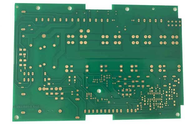
6layer PCB Stack-up
The 6 layer PCB standard stackup includes 4 routing layers and 2 extra signal layers added between the planes.
SMTFAB is a valuable PCB fabrication company with a competitive price for 6 layer PCB. You will count on us to provide top quality and deliver in time.
The 6 layer PCB stackup is more complicated than 4 layer stackup. Typically, we recommend our customers to use FR4 Middle TG(TG150) for over 6 layer multilayer PCBs. It will avoid some potential quality issues during the PCB assembly.
You will see the specifications from our 6 layer PCB stackup. The board thickness is from 0.4mm to 4.0mm, the copper thickness of the outer layer for 6 layer PCB stackup is from 35um to 420um, and the copper thickness of the inner layer is from 18um to 175um.
If you are looking for a leading supplier for 6 layer PCB stackup, you have come at the right price. Our engineers can offer you a custom 6 layer PCB stackup. With the right 6 layer PCB stackup, you can suppress Electro-Magnetic Interference(EMI) between different layers.
SMTFAB as one of your best partners can offer a one-stop solution for you, so it’s not necessary for you to find several suppliers for 6 layer PCB stackup design and manufacture.
Just contact us now when you are ready.
6 Layer PCB Stackup: The Ultimate FAQ Guide
The 6 layer PCB stackup is a standard 4-layer stackup with two additional layers. It has 4 routing layers (2 inside and 2 outside) and 2 inner planes (1 for power and the other for ground). They can produce a high-performance multilayer PCB using dependable predefined mutual connections.
We are a professional 6 layer PCB stackup designer and have been working in this field for more than 15 years. From our experience, we have decided to share some of our knowledge with you.
- What Does A 6 Layer PCB Stackup Mean?
- Which Quality Certifications Certify A 6 Layer PCB StackUp?
- What Are The Design Factors Of 6 Layer PCB StackUp?
- Why Are Dielectrics Significant In 6 Layer PCB StackUp?
- What Advantages Does 6 Layer PCB StackUp Provide?
- What Factors Determine The Purchase Cost Of A 6Layer PCB StackUp?
- What Are The Comparisons Between A 6 Layer PCB Stack Up And A 4 Layer PCB Stack Up?
- How Glass Transition Temperature Impacts A 6 Layer PCB StackUp?
- Why Is 6 Layer PCB StackUp Design Significant?
- What Is The Configuration On The 6 Layer PCB Stack Up?
- What Are The Limitations Of 6 Layer PCB StackUp?
- How Many Signal, Ground, And Power Plans Will You Need For 6 Layer PCB StackUp?
- How To Route Between Multiple Layers Of 6 Layer PCB StackUp?
- How Thick Is A 6 Layer PCB StackUp?
- Is It Possible To Use Custom Design In 6 Layer PCB StackUp?
- What Is The Manufacturing Process Of 6 Layer PCB Stack Up?
- Which Industries Use The 6 Layer PCB StackUp?
- How Should You Select The Right 6 Layer PCB StackUp?
- What Types Of Vias Are Available In The 6 Layer PCB StackUp?
What Does A 6 Layer PCB Stackup Mean?
6 layer PCB stackup is a typical 4 layer PCB stackup with 2 additional layers. It consists of 4 routing layers(2 each for internal and outer layers) and 2 inner planes. This stackup process dramatically increases Electromagnetic interference (EMI).

6 layer PCB stackup
If you have a 4-layer printed circuit board stack up, you can easily convert it to a 6 layer PCB stack-up simply by adding 2 additional signal layers.
Which Quality Certifications Certify A 6 Layer PCB StackUp?
You must ensure the 6 layer PCB stackup must be of the highest quality. Sticking with quality certification is the only way you can achieve that.
The standard of your 6 layer PCB stackup will depend on the quality certification.
You have to follow the following quality certifications to certify the quality of your 6 layer PCB stackup.
- CE Certification
- UL Certification
- AHRI/ ANSI Certifications
- RoHS Certification
- IATF Certifications like IATF 16949
What Are The Design Factors Of 6 Layer PCB StackUp?
This stackup design can be a difficult task for somebody. But if you follow the factors that consist of the design specifications, that should not be that tough.

6 Layer PCB Stackup
Or, we can say those special considerations will guide your design process.
Here are some factors you should consider when you design your 6 layer PCB stackup.
Application Area
A 6 layer PCB stackup can perform various applications effectively and efficiently, and you can use those PCBs in multiple sectors.
Consequently, you should pick your industry first you will use your 6 layer PCB stackup at the beginning of your design.
Design And Production Cost
After you have selected the application, you should consider the production cost as well. Remember, the designing cost is proportional to the complexity of your 6 layer PCB stackup.

6 layer PCB Design
Design Configuration
Now that you have decided on the application type and the cost, it’s time to structure the board’s layout.
There are a vast number of 6 layer printing circuit board stackup configurations to choose from. You will select the design according to your requirements.
Component Density
It would be best to regulate the density of the components you are going to use because the 6layer PCB stackup can determine multiple electrical connections.
You should consider the types of components and the number you are going to mount on the 6layer PCB stackup.
Thermal Specifications
You are going to use your 6 layer PCB stackup in various projects, and most of them will require high temperatures.
Therefore, considering each aspect of thermal identification and specification during your design process is imperative.
Electrical Specifications
This is a crucial factor, and that is the amount of current that will pass through at a specific moment on your 6layer PCB stackup. If you know that number, you can provide the proper signal paths and routes for the current to flow efficiently.
Know more about the 6 layer PCB stackup design from this video
Why Are Dielectrics Significant In 6 Layer PCB StackUp?
You can not conduct electricity using dielectric systems when they are in their fundamental formation.
You can provide electrical cater electrical isolation using dielectric materials on your 6 layer PCB. This is a handy component and produces electrical isolation to copper or other conductive materials.

Dielectric Material Properties
Following materials are highly used dielectric materials that you will find on 6-layer PCBs:
- Plastic Materials
- Aluminum Oxide Materials
- Glass Materials
- Paper Materials
- Porcelain Materials
You need to control the frequency levels and operating temperatures to determine the dielectric material’s performance.
Besides, you have to evaluate the electrical, thermal, chemical, and mechanical properties.
These factors will primarily control the dielectric material’s performance on your 6-layer PCB stack up.
What Advantages Does 6 Layer PCB StackUp Provide?
You will find these in many applications that you use in your daily life because of the advantages they bring to the PCB boards. Let us discuss the benefits that you can get from a 6 layer PCB stackup.
Connection Processes Are More Simplified
You can make different machines’ connection processes more simplified with the help of a 6 layer PCB stackup—no need to waste valuable materials and spaces when you are developing more significant devices.
Easy Maintenance
This is the most crucial advantage you will get from 6 layer PCB stack-ups; they are durable and require minimal maintenance.
If there is no unlikely damage, you can easily rework your 6 layer PCB stackup.
Simple Layouts
The navigation through the 6 layer PCB stack-up structure is effortless because of the layout. 6 layer PCB stackup comes with a pretty straightforward layout and clear silk screen labels.
Dependable
The efficiency and reliability of this PCB stack up are undoubted. These PCBs face various tests and inspections and are fixed before they reach the market.
Reduces The Production Cost
In a 6 layer PCB stack up, you will need fewer components which reduces the production cost significantly. As this PCB requires fewer components, you have to purchase fewer components, and consequently, the production cost reduces.
What Factors Determine The Purchase Cost Of A 6Layer PCB StackUp?
Many factors can influence the purchase cost of a 6-layer Printed circuit board stack up.
We have mentioned the thumb rule earlier but let us remind you again, the higher the complexity, the higher the price of a 6 layer PCB stackup. So, a more complex one will cost you more, but that is not the only factor. Here are some of those:
● Components Quality
The quality of the components you are going to use in your 6 layer PCB stackup will definitely affect the price. High-quality components will cost you more.
● Quantity Of The Components
It is eminent that if the number of components increases, the price will automatically increase. But one thing you should consider here. When the number of components increases in a 6 layer PCB stackup, that automatically makes the PCB complex. And remember what we mentioned earlier? A complex 6 layer PCB stack up will cost you more.
● Dimensions
The dimensions also influence the 6-layer PCB stack-up price. A higher dimension will make the PCB bigger, and that will cost more than other ones.
And lastly, the manufacturer of your 6 layer PCB stackup can reduce the cost significantly.
What Are The Comparisons Between A 6 Layer PCB Stack Up And A 4 Layer PCB Stack Up?
Noticing the name, you can understand that a 4-layer PCB stack-up has fewer layers than a 6 layer PCB stackup. Or, we can say that a 6 layer PCB stackup is an updated version of a 4-layer PCB stack-up.
We can say the word ‘updated’ because you will find 2 extra signal layers in-between planes of a 6 layer PCB stackup. And that also increases the purchase cost of a 6 layer PCB stackup.
Apart from that, a 6-layer PCB stack up comes with lower impedance if we compare it with a 4-layer PCB stack up.
Another critical difference is the wire connection. A 6-layer PCB stack-up has more space and therefore comes with less wire connection on each layer than a 4-layer PCB stack up.
And lastly, a 6 layer PCB stackup works more efficiently and performs better than a 4-layer PCB stackup.
How Does Glass Transition Temperature Impacts A 6 Layer PCB StackUp?
Thermal property is a crucial factor that you should look after while designing your 6 layer PCB stackup.
The behavior of your 6 layer PCB stackup, when exposed to heat, depends on its thermal property. And the glass transition temperature is primarily responsible for determining the thermal property of the materials under excessive temperature.

Glass Transition Temperature
What is the glass transition temperature? It is the highest temperature where a solid glass can stay stable without changing its physical properties. And with this temperature, you can note the highest temperature that you can not exceed during the manufacturing process.
If you exceed this glass transition temperature, materials like hard glass will still remain solid, but they will change their physical property and become rubber-like materials.
Why Is 6 Layer PCB StackUp Design Significant?
At the core of making smaller and better components, there is a multi-core PCB. 6 layer printed circuit board stack up that helped to place additional circuit traces in the past.
But these days, the application of 6 layer PCB stack-ups has changed, and now they are more vital for creating better layer configurations and providing optimal performance.
These PCBs also reduce the chance of electromagnetic interference that typically happens because of poor signal performance.
The 6 layer PCB stackup also can eliminate impedance and crosstalk problems, and this way, they improve reliability which is a fundamental PCB property.
Apart from that, it is highly dependable in reducing the external source of noise, making it a better option.
Fundamentals of PCB stack-up design
What Is The Configuration On The 6 Layer PCB Stack Up?
The configuration of your 6 layer PCB stackup varies, and it depends on the application you are working on.
Suppose you are configuring for a control signal; in that case, you will need more layers. On the contrary, if you are planning high-speed circuitry, you will have to configure it for the best protection.

6 layer Rigid-flex PCB Stackup
Below is the main 6 layer PCB stackup configuration you can opt for:
- Top
- Inner
- Ground
- Power
- Inner
- Bottom
This configuration is not the most common one as it can not shield signal layers properly.
Here is another 6 layer PCB stackup configuration you can opt for:
- Top
- Ground
- Inner
- Inner
- Power
- Bottom
This configuration is better as it protects the inner layer more efficiently.
For those PCBs that operate on high signals, this is the best configuration.
What Are The Limitations Of 6 Layer PCB StackUp?
Like every other PCB stack up, the 6 layer PCB stackup also has its limitations. Here are some hurdles that you will face with a 6 layer PCB stackup:
Costly Production
High performance demands high value. As a 6 layer PCB stackup is more efficient and provides many advantages, the manufacturing cost is also too high.
Compared to a 4-layer PCB stack up, your 6 layer PCB stackup production will cost more.
Varying Configurations
The configuration is crucial for a 6 layer PCB stackup. A suitable configuration will provide you with better performance. But if you employ the wrong format, that will give more problems than positive results.
This is significant because the 6 layer PCB stackup wrong configuration will cause more problems.
How Many Signal, Ground, And Power Plans Will You Need For 6 Layer PCB StackUp?
The requirement of signals, grounds, and power plans you are going to need depends on the application type.
If you are routing thick boards and the space is really small, you will need the following:
- 4Signal
- 1Ground
- 1Power
When you are concerned about the susceptibility to EMI of your 6 layer PCB stackup, you will require more ground and few signals.
The performance will depend on how you arrange the planes on it.

PCB Power And Ground Plane
Here are some available options that you can apply:
Signal Layer/Ground Plane/two signal layers/Power plane/Signal Layer
Ground Plane/Signal Layer/Ground Plane/Power Plane/Ground Plane/Signal Layer
Ground Plan/Signal Layer/Ground Plane/Power Plane/Sigal Layer/Ground Plane
How To Route Between Multiple Layers Of 6 Layer PCB StackUp?
While routing in the middle of multiple layers on your 6 layer PCB stackup, there are few options for you to choose from.
Decoupling capacitors keeping parallel to the signal vias is one option that you can opt for.
This will help to create a proper return path for the signal and boost the reliability and overall performance of your 6 layer PCB stackup.
Moreover, you can put the signal vias to pass adjacent to the ground vias with similar types of reference planes.
It will make a shallow induction return path that will not affect the coupling to reference planes.
And the bypass capacitors will establish a direct connection to the reference planes as vias or signal traces.
This will help to reduce the supply voltage fluctuation and produce charge reservoirs.
Besides, it creates an ideal path for induced returns that can happen for transmission and signals between various layers.
How Thick Is A 6 Layer PCB StackUp?
The 6 layer PCB stackup thickness is not fixed and varies considerably. So, you will have to work with 6 layer PCB stackups of various thicknesses according to the application type.
Typically the component materials’ thickness is the primary consideration for a 6 layer PCB stackup’s thickness.
The standard thickness for your 6 layer PCB stackup ranges from .7mm t 3.0 mm. Various layer arrangements will determine the thickness of your 6 layer PCB stackup. Besides, the thickness will also vary for the materials you are going to use in your design.
Is It Possible To Use Custom Design In 6 Layer PCB StackUp?
Absolutely. You can use your absolute freedom when you are designing your 6 layer PCB stackups.
The design depends on the application type, and you can use your creativity in design.
In SMTFAB, we produce custom and unique designs that you can use for your 6 layer PCB stackup.
What Is The Manufacturing Process Of 6 Layer PCB Stack Up?
The manufacturing process of a 6 layer PCB stackup is not that complicated, and you can use the following steps to manufacture your 6 layer PCB stackup design.
First Step: Design
The first step is designing. You have put your ideas in a design first. You will design according to the application specifications. Don’t forget to insert each feature on the design of your 6 layer PCB stackup design you want to present in the final product.
When you are done with your design, you have to test the design to confirm that everything is in the right place and you did not miss anything.
Second Step: Preparation
After finishing the design, it’s time to produce the blueprint of your design. The blueprint of your 6-layer PCB stack up will guide the entire manufacturing process. The blueprint establishes all the materials you are going to use in the manufacturing process.
You can use the BOM or Bill of Materials to make the job simple, and that helps you to plan every material precisely. The BOM also helps you with every detail of the proper machine you are going to use in your manufacturing process.
Third Step: Begin The Manufacturing
Now, if everything is done perfectly, it’s time to begin the manufacturing process. You have to start with cutting all the materials according to the right dimensions.
You have to make each layer separately based on the arrangement of your 6 layer PCB stackup. Ensure that each layer gets the correct coating and then execute the image exposure.
Then it’s time for image development and inner layers etching. When these steps are done, apply the resist strip.
Before you go for oxide coating, there is another step to perform. It would be best if you used AOI or automated optical inspection.
After you are done with each layer, arranging them is the final step. You will put one layer on top of another according to your design and laminate together. And that will complete your 6-layer PCB stack up the manufacturing process.
Which Industries Use The 6 Layer PCB StackUp?
As we mentioned earlier, the 6 layer PCB stackup is widely used in various types of applications. You can arrange and configure a 6 layer PCB stackup to different kinds of applications.
Remember each 6-layer printed circuit board stack-up has unique arrangements and is manufactured for specific application requirements.
Here are some applications of 6 layer PCB stackup:
- The medical industry depends on a 6 layer PCB stackup largely. There are many medical types of equipment that use 6 layer PCB stackups.
- Many types of vehicle parts in the automotive industry are made of 6 layer PCB stackups.
- Cellphones and any other communication devices are made of 6 layer PCB stackups. The communication industry is a big consumer of the 66 layer PCB stackup.
- Machine controlling machines of the processing industry are made of the 6 layer PCB stackup.

6-Layer PCB Are Widely Used In Medical Industry
How Should You Select The Right 6 Layer PCB StackUp?
The best way of picking the perfect 6 layer PCB stackup for your application is the specifications of the 6 layer PCB stackup you are intending to purchase.
So, at first, you need to know the exact demand of your application and then find a 6 layer PCB stackup with appropriate specifications.
Below are some of the properties that you can look at while choosing your 6 layer PCB stackup:
- Chemical Properties
- Electrical Properties
- Mechanical Properties
- Thermal Properties
What Types Of Vias Are Available In The 6 Layer PCB StackUp?
The vias you will choose for your 6 layer PCB stackup will depend on your application type. For assistance, we have listed the following types of vias you can use for your 6 layer PCB stackup.
Through-hole vias: These vias will penetrate from the top of your stack up all the way to the bottom.

Types of Vias
Blind Vias: These vias start from the outer layer and end up in an internal layer.
Hidden or Buried Vias: It works between internal layers.
Micro Vias: As the name suggests, they are very small in size.
Vias in Pad: You will find these vias with the pads.
Final Words
The 6 layer PCB stackup is versatile, and you can use them in various types of applications. If the design, configuration, and manufacturing process are alright, the 6 layer PCB stackup can be very handy. We hope the guide has helped you. If you did not find what you are looking for or want to know more, don’t hesitate to contact our experts.
Your Best 6 Layer PCB Stackup Manufacturer in China
SMTFAB is a professional 6 layer PCB stackup manufacturer in China, we could provide different types of 6 layer PCB stackup for your project.
- Over 12 years 6 layer PCB stackup design experience
- From rigid PCB, flexible PCB, and rigid-flexible PCB
- The USA and Canada UL Certificated
- No minimum order quantity for your new order
- Top-quality and 100% E-test
- 7/24 sales and engineering tech support
- Production Facility
- Capabilities
| Feature | Capability |
| Quality Grade | Standard IPC 2 and IPC 3 |
| Number of Layers | 2 – 40layers |
| Order Quantity | 1pc – 1Million+pcs |
| Build Time | 24H – 4weeks |
| Material | S1150G, S1165, S1000-2 |
| Board Size | Min 5*5mm | Max 500*650mm |
| Board Thickness | 0.4mm – 6.5mm |
| Copper Weight (Finished) | 0.5oz – 10.0oz |
| Min Tracing/Spacing | 3mil/3mil |
| Solder Mask Sides | As per the file |
| Solder Mask Color | Green, White, Blue, Black, Red, Yellow |
| Silkscreen Sides | As per the file |
| Silkscreen Color | White, Black, Yellow |
| Surface Finish | HASL – Hot Air Solder Leveling |
| Lead-Free HASL – RoHS | |
| ENIG – Electroless Nickle/Immersion Gold – RoHS | |
| Immersion Silver – RoHS | |
| Immersion Tin – RoHS | |
| OSP – Organic Solderability Preservatives – RoHS | |
| Min Annular Ring | 4mil |
| Min Drilling Hole Diameter | 6mil |
| Other Techniques | Gold fingers |
| Blind/Buried Vias |
Releted Some Other PCBs
Why Choose SMTFAB for Your 6 Layer PCB Stackup
6 layer PCB is an economical and popular stackup for many applications. There are high net counts and small sizes.
As an experienced manufacturer of 6 layer PCB stackup, SMTFAB has one professional engineering team and they have more than 20 working experiences in PCB-related industries. Some of them had worked for famous companies like Foxconn, Huawei, or TTM. They have rich experience and provide professional suggestions for your project.
6layer PCB Stack-up
The 6 layer PCB standard stackup includes 4 routing layers and 2 extra signal layers added between the planes.
SMTFAB is a valuable PCB fabrication company with a competitive price for 6 layer PCB. You will count on us to provide top quality and deliver in time.
The 6 layer PCB stackup is more complicated than 4 layer stackup. Typically, we recommend our customers to use FR4 Middle TG(TG150) for over 6 layer multilayer PCBs. It will avoid some potential quality issues during the PCB assembly.
You will see the specifications from our 6 layer PCB stackup. The board thickness is from 0.4mm to 4.0mm, the copper thickness of the outer layer for 6 layer PCB stackup is from 35um to 420um, and the copper thickness of the inner layer is from 18um to 175um.
If you are looking for a leading supplier for 6 layer PCB stackup, you have come at the right price. Our engineers can offer you a custom 6 layer PCB stackup. With the right 6 layer PCB stackup, you can suppress Electro-Magnetic Interference(EMI) between different layers.
SMTFAB as one of your best partners can offer a one-stop solution for you, so it’s not necessary for you to find several suppliers for 6 layer PCB stackup design and manufacture.
Just contact us now when you are ready.
6 Layer PCB Stackup: The Ultimate FAQ Guide
The 6 layer PCB stackup is a standard 4-layer stackup with two additional layers. It has 4 routing layers (2 inside and 2 outside) and 2 inner planes (1 for power and the other for ground). They can produce a high-performance multilayer PCB using dependable predefined mutual connections.
We are a professional 6 layer PCB stackup designer and have been working in this field for more than 15 years. From our experience, we have decided to share some of our knowledge with you.
- What Does A 6 Layer PCB Stackup Mean?
- Which Quality Certifications Certify A 6 Layer PCB StackUp?
- What Are The Design Factors Of 6 Layer PCB StackUp?
- Why Are Dielectrics Significant In 6 Layer PCB StackUp?
- What Advantages Does 6 Layer PCB StackUp Provide?
- What Factors Determine The Purchase Cost Of A 6Layer PCB StackUp?
- What Are The Comparisons Between A 6 Layer PCB Stack Up And A 4 Layer PCB Stack Up?
- How Glass Transition Temperature Impacts A 6 Layer PCB StackUp?
- Why Is 6 Layer PCB StackUp Design Significant?
- What Is The Configuration On The 6 Layer PCB Stack Up?
- What Are The Limitations Of 6 Layer PCB StackUp?
- How Many Signal, Ground, And Power Plans Will You Need For 6 Layer PCB StackUp?
- How To Route Between Multiple Layers Of 6 Layer PCB StackUp?
- How Thick Is A 6 Layer PCB StackUp?
- Is It Possible To Use Custom Design In 6 Layer PCB StackUp?
- What Is The Manufacturing Process Of 6 Layer PCB Stack Up?
- Which Industries Use The 6 Layer PCB StackUp?
- How Should You Select The Right 6 Layer PCB StackUp?
- What Types Of Vias Are Available In The 6 Layer PCB StackUp?
What Does A 6 Layer PCB Stackup Mean?
6 layer PCB stackup is a typical 4 layer PCB stackup with 2 additional layers. It consists of 4 routing layers(2 each for internal and outer layers) and 2 inner planes. This stackup process dramatically increases Electromagnetic interference (EMI).
6 layer PCB stackup
If you have a 4-layer printed circuit board stack up, you can easily convert it to a 6 layer PCB stack-up simply by adding 2 additional signal layers.
Which Quality Certifications Certify A 6 Layer PCB StackUp?
You must ensure the 6 layer PCB stackup must be of the highest quality. Sticking with quality certification is the only way you can achieve that.
The standard of your 6 layer PCB stackup will depend on the quality certification.
You have to follow the following quality certifications to certify the quality of your 6 layer PCB stackup.
- CE Certification
- UL Certification
- AHRI/ ANSI Certifications
- RoHS Certification
- IATF Certifications like IATF 16949
What Are The Design Factors Of 6 Layer PCB StackUp?
This stackup design can be a difficult task for somebody. But if you follow the factors that consist of the design specifications, that should not be that tough.
6 Layer PCB Stackup
Or, we can say those special considerations will guide your design process.
Here are some factors you should consider when you design your 6 layer PCB stackup.
Application Area
A 6 layer PCB stackup can perform various applications effectively and efficiently, and you can use those PCBs in multiple sectors.
Consequently, you should pick your industry first you will use your 6 layer PCB stackup at the beginning of your design.
Design And Production Cost
After you have selected the application, you should consider the production cost as well. Remember, the designing cost is proportional to the complexity of your 6 layer PCB stackup.
6 layer PCB Design
Design Configuration
Now that you have decided on the application type and the cost, it’s time to structure the board’s layout.
There are a vast number of 6 layer printing circuit board stackup configurations to choose from. You will select the design according to your requirements.
Component Density
It would be best to regulate the density of the components you are going to use because the 6layer PCB stackup can determine multiple electrical connections.
You should consider the types of components and the number you are going to mount on the 6layer PCB stackup.
Thermal Specifications
You are going to use your 6 layer PCB stackup in various projects, and most of them will require high temperatures.
Therefore, considering each aspect of thermal identification and specification during your design process is imperative.
Electrical Specifications
This is a crucial factor, and that is the amount of current that will pass through at a specific moment on your 6layer PCB stackup. If you know that number, you can provide the proper signal paths and routes for the current to flow efficiently.
Know more about the 6 layer PCB stackup design from this video
Why Are Dielectrics Significant In 6 Layer PCB StackUp?
You can not conduct electricity using dielectric systems when they are in their fundamental formation.
You can provide electrical cater electrical isolation using dielectric materials on your 6 layer PCB. This is a handy component and produces electrical isolation to copper or other conductive materials.
Dielectric Material Properties
Following materials are highly used dielectric materials that you will find on 6-layer PCBs:
- Plastic Materials
- Aluminum Oxide Materials
- Glass Materials
- Paper Materials
- Porcelain Materials
You need to control the frequency levels and operating temperatures to determine the dielectric material’s performance.
Besides, you have to evaluate the electrical, thermal, chemical, and mechanical properties.
These factors will primarily control the dielectric material’s performance on your 6-layer PCB stack up.
What Advantages Does 6 Layer PCB StackUp Provide?
You will find these in many applications that you use in your daily life because of the advantages they bring to the PCB boards. Let us discuss the benefits that you can get from a 6 layer PCB stackup.
Connection Processes Are More Simplified
You can make different machines’ connection processes more simplified with the help of a 6 layer PCB stackup—no need to waste valuable materials and spaces when you are developing more significant devices.
Easy Maintenance
This is the most crucial advantage you will get from 6 layer PCB stack-ups; they are durable and require minimal maintenance.
If there is no unlikely damage, you can easily rework your 6 layer PCB stackup.
Simple Layouts
The navigation through the 6 layer PCB stack-up structure is effortless because of the layout. 6 layer PCB stackup comes with a pretty straightforward layout and clear silk screen labels.
Dependable
The efficiency and reliability of this PCB stack up are undoubted. These PCBs face various tests and inspections and are fixed before they reach the market.
Reduces The Production Cost
In a 6 layer PCB stack up, you will need fewer components which reduces the production cost significantly. As this PCB requires fewer components, you have to purchase fewer components, and consequently, the production cost reduces.
What Factors Determine The Purchase Cost Of A 6Layer PCB StackUp?
Many factors can influence the purchase cost of a 6-layer Printed circuit board stack up.
We have mentioned the thumb rule earlier but let us remind you again, the higher the complexity, the higher the price of a 6 layer PCB stackup. So, a more complex one will cost you more, but that is not the only factor. Here are some of those:
● Components Quality
The quality of the components you are going to use in your 6 layer PCB stackup will definitely affect the price. High-quality components will cost you more.
● Quantity Of The Components
It is eminent that if the number of components increases, the price will automatically increase. But one thing you should consider here. When the number of components increases in a 6 layer PCB stackup, that automatically makes the PCB complex. And remember what we mentioned earlier? A complex 6 layer PCB stack up will cost you more.
● Dimensions
The dimensions also influence the 6-layer PCB stack-up price. A higher dimension will make the PCB bigger, and that will cost more than other ones.
And lastly, the manufacturer of your 6 layer PCB stackup can reduce the cost significantly.
What Are The Comparisons Between A 6 Layer PCB Stack Up And A 4 Layer PCB Stack Up?
Noticing the name, you can understand that a 4-layer PCB stack-up has fewer layers than a 6 layer PCB stackup. Or, we can say that a 6 layer PCB stackup is an updated version of a 4-layer PCB stack-up.
We can say the word ‘updated’ because you will find 2 extra signal layers in-between planes of a 6 layer PCB stackup. And that also increases the purchase cost of a 6 layer PCB stackup.
Apart from that, a 6-layer PCB stack up comes with lower impedance if we compare it with a 4-layer PCB stack up.
Another critical difference is the wire connection. A 6-layer PCB stack-up has more space and therefore comes with less wire connection on each layer than a 4-layer PCB stack up.
And lastly, a 6 layer PCB stackup works more efficiently and performs better than a 4-layer PCB stackup.
How Does Glass Transition Temperature Impacts A 6 Layer PCB StackUp?
Thermal property is a crucial factor that you should look after while designing your 6 layer PCB stackup.
The behavior of your 6 layer PCB stackup, when exposed to heat, depends on its thermal property. And the glass transition temperature is primarily responsible for determining the thermal property of the materials under excessive temperature.
Glass Transition Temperature
What is the glass transition temperature? It is the highest temperature where a solid glass can stay stable without changing its physical properties. And with this temperature, you can note the highest temperature that you can not exceed during the manufacturing process.
If you exceed this glass transition temperature, materials like hard glass will still remain solid, but they will change their physical property and become rubber-like materials.
Why Is 6 Layer PCB StackUp Design Significant?
At the core of making smaller and better components, there is a multi-core PCB. 6 layer printed circuit board stack up that helped to place additional circuit traces in the past.
But these days, the application of 6 layer PCB stack-ups has changed, and now they are more vital for creating better layer configurations and providing optimal performance.
These PCBs also reduce the chance of electromagnetic interference that typically happens because of poor signal performance.
The 6 layer PCB stackup also can eliminate impedance and crosstalk problems, and this way, they improve reliability which is a fundamental PCB property.
Apart from that, it is highly dependable in reducing the external source of noise, making it a better option.
Fundamentals of PCB stack-up design
What Is The Configuration On The 6 Layer PCB Stack Up?
The configuration of your 6 layer PCB stackup varies, and it depends on the application you are working on.
Suppose you are configuring for a control signal; in that case, you will need more layers. On the contrary, if you are planning high-speed circuitry, you will have to configure it for the best protection.
6 layer Rigid-flex PCB Stackup
Below is the main 6 layer PCB stackup configuration you can opt for:
- Top
- Inner
- Ground
- Power
- Inner
- Bottom
This configuration is not the most common one as it can not shield signal layers properly.
Here is another 6 layer PCB stackup configuration you can opt for:
- Top
- Ground
- Inner
- Inner
- Power
- Bottom
This configuration is better as it protects the inner layer more efficiently.
For those PCBs that operate on high signals, this is the best configuration.
What Are The Limitations Of 6 Layer PCB StackUp?
Like every other PCB stack up, the 6 layer PCB stackup also has its limitations. Here are some hurdles that you will face with a 6 layer PCB stackup:
Costly Production
High performance demands high value. As a 6 layer PCB stackup is more efficient and provides many advantages, the manufacturing cost is also too high.
Compared to a 4-layer PCB stack up, your 6 layer PCB stackup production will cost more.
Varying Configurations
The configuration is crucial for a 6 layer PCB stackup. A suitable configuration will provide you with better performance. But if you employ the wrong format, that will give more problems than positive results.
This is significant because the 6 layer PCB stackup wrong configuration will cause more problems.
How Many Signal, Ground, And Power Plans Will You Need For 6 Layer PCB StackUp?
The requirement of signals, grounds, and power plans you are going to need depends on the application type.
If you are routing thick boards and the space is really small, you will need the following:
- 4Signal
- 1Ground
- 1Power
When you are concerned about the susceptibility to EMI of your 6 layer PCB stackup, you will require more ground and few signals.
The performance will depend on how you arrange the planes on it.
PCB Power And Ground Plane
Here are some available options that you can apply:
Signal Layer/Ground Plane/two signal layers/Power plane/Signal Layer
Ground Plane/Signal Layer/Ground Plane/Power Plane/Ground Plane/Signal Layer
Ground Plan/Signal Layer/Ground Plane/Power Plane/Sigal Layer/Ground Plane
How To Route Between Multiple Layers Of 6 Layer PCB StackUp?
While routing in the middle of multiple layers on your 6 layer PCB stackup, there are few options for you to choose from.
Decoupling capacitors keeping parallel to the signal vias is one option that you can opt for.
This will help to create a proper return path for the signal and boost the reliability and overall performance of your 6 layer PCB stackup.
Moreover, you can put the signal vias to pass adjacent to the ground vias with similar types of reference planes.
It will make a shallow induction return path that will not affect the coupling to reference planes.
And the bypass capacitors will establish a direct connection to the reference planes as vias or signal traces.
This will help to reduce the supply voltage fluctuation and produce charge reservoirs.
Besides, it creates an ideal path for induced returns that can happen for transmission and signals between various layers.
How Thick Is A 6 Layer PCB StackUp?
The 6 layer PCB stackup thickness is not fixed and varies considerably. So, you will have to work with 6 layer PCB stackups of various thicknesses according to the application type.
Typically the component materials’ thickness is the primary consideration for a 6 layer PCB stackup’s thickness.
The standard thickness for your 6 layer PCB stackup ranges from .7mm t 3.0 mm. Various layer arrangements will determine the thickness of your 6 layer PCB stackup. Besides, the thickness will also vary for the materials you are going to use in your design.
Is It Possible To Use Custom Design In 6 Layer PCB StackUp?
Absolutely. You can use your absolute freedom when you are designing your 6 layer PCB stackups.
The design depends on the application type, and you can use your creativity in design.
In SMTFAB, we produce custom and unique designs that you can use for your 6 layer PCB stackup.
What Is The Manufacturing Process Of 6 Layer PCB Stack Up?
The manufacturing process of a 6 layer PCB stackup is not that complicated, and you can use the following steps to manufacture your 6 layer PCB stackup design.
First Step: Design
The first step is designing. You have put your ideas in a design first. You will design according to the application specifications. Don’t forget to insert each feature on the design of your 6 layer PCB stackup design you want to present in the final product.
When you are done with your design, you have to test the design to confirm that everything is in the right place and you did not miss anything.
Second Step: Preparation
After finishing the design, it’s time to produce the blueprint of your design. The blueprint of your 6-layer PCB stack up will guide the entire manufacturing process. The blueprint establishes all the materials you are going to use in the manufacturing process.
You can use the BOM or Bill of Materials to make the job simple, and that helps you to plan every material precisely. The BOM also helps you with every detail of the proper machine you are going to use in your manufacturing process.
Third Step: Begin The Manufacturing
Now, if everything is done perfectly, it’s time to begin the manufacturing process. You have to start with cutting all the materials according to the right dimensions.
You have to make each layer separately based on the arrangement of your 6 layer PCB stackup. Ensure that each layer gets the correct coating and then execute the image exposure.
Then it’s time for image development and inner layers etching. When these steps are done, apply the resist strip.
Before you go for oxide coating, there is another step to perform. It would be best if you used AOI or automated optical inspection.
After you are done with each layer, arranging them is the final step. You will put one layer on top of another according to your design and laminate together. And that will complete your 6-layer PCB stack up the manufacturing process.
Which Industries Use The 6 Layer PCB StackUp?
As we mentioned earlier, the 6 layer PCB stackup is widely used in various types of applications. You can arrange and configure a 6 layer PCB stackup to different kinds of applications.
Remember each 6-layer printed circuit board stack-up has unique arrangements and is manufactured for specific application requirements.
Here are some applications of 6 layer PCB stackup:
- The medical industry depends on a 6 layer PCB stackup largely. There are many medical types of equipment that use 6 layer PCB stackups.
- Many types of vehicle parts in the automotive industry are made of 6 layer PCB stackups.
- Cellphones and any other communication devices are made of 6 layer PCB stackups. The communication industry is a big consumer of the 66 layer PCB stackup.
- Machine controlling machines of the processing industry are made of the 6 layer PCB stackup.
6-Layer PCB Are Widely Used In Medical Industry
How Should You Select The Right 6 Layer PCB StackUp?
The best way of picking the perfect 6 layer PCB stackup for your application is the specifications of the 6 layer PCB stackup you are intending to purchase.
So, at first, you need to know the exact demand of your application and then find a 6 layer PCB stackup with appropriate specifications.
Below are some of the properties that you can look at while choosing your 6 layer PCB stackup:
- Chemical Properties
- Electrical Properties
- Mechanical Properties
- Thermal Properties
What Types Of Vias Are Available In The 6 Layer PCB StackUp?
The vias you will choose for your 6 layer PCB stackup will depend on your application type. For assistance, we have listed the following types of vias you can use for your 6 layer PCB stackup.
Through-hole vias: These vias will penetrate from the top of your stack up all the way to the bottom.
Types of Vias
Blind Vias: These vias start from the outer layer and end up in an internal layer.
Hidden or Buried Vias: It works between internal layers.
Micro Vias: As the name suggests, they are very small in size.
Vias in Pad: You will find these vias with the pads.
Final Words
The 6 layer PCB stackup is versatile, and you can use them in various types of applications. If the design, configuration, and manufacturing process are alright, the 6 layer PCB stackup can be very handy. We hope the guide has helped you. If you did not find what you are looking for or want to know more, don’t hesitate to contact our experts.
Your Best 6 Layer PCB Stackup Manufacturer in China
SMTFAB is a professional 6 layer PCB stackup manufacturer in China, we could provide different types of 6 layer PCB stackup for your project.
- Over 12 years 6 layer PCB stackup design experience
- From rigid PCB, flexible PCB, and rigid-flexible PCB
- The USA and Canada UL Certificated
- No minimum order quantity for your new order
- Top-quality and 100% E-test
- 7/24 sales and engineering tech support
Your Best 6 Layer PCB Stackup Manufacturer in China
Your Best 6 Layer PCB Stackup Manufacturer in China
SMTFAB is a professional 6 layer PCB stackup manufacturer in China, we could provide different types of 6 layer PCB stackup for your project.
- Over 12 years 6 layer PCB stackup design experience
- From rigid PCB, flexible PCB, and rigid-flexible PCB
- The USA and Canada UL Certificated
- No minimum order quantity for your new order
- Top-quality and 100% E-test
- 7/24 sales and engineering tech support
- Production Facility
- Capabilities
| Feature | Capability |
| Quality Grade | Standard IPC 2 and IPC 3 |
| Number of Layers | 2 – 40layers |
| Order Quantity | 1pc – 1Million+pcs |
| Build Time | 24H – 4weeks |
| Material | S1150G, S1165, S1000-2 |
| Board Size | Min 5*5mm | Max 500*650mm |
| Board Thickness | 0.4mm – 6.5mm |
| Copper Weight (Finished) | 0.5oz – 10.0oz |
| Min Tracing/Spacing | 3mil/3mil |
| Solder Mask Sides | As per the file |
| Solder Mask Color | Green, White, Blue, Black, Red, Yellow |
| Silkscreen Sides | As per the file |
| Silkscreen Color | White, Black, Yellow |
| Surface Finish | HASL – Hot Air Solder Leveling |
| Lead-Free HASL – RoHS | |
| ENIG – Electroless Nickle/Immersion Gold – RoHS | |
| Immersion Silver – RoHS | |
| Immersion Tin – RoHS | |
| OSP – Organic Solderability Preservatives – RoHS | |
| Min Annular Ring | 4mil |
| Min Drilling Hole Diameter | 6mil |
| Other Techniques | Gold fingers |
| Blind/Buried Vias |
Releted Some Other PCBs
Releted Some Other PCBs
Why Choose SMTFAB for Your 6 Layer PCB Stackup
6 layer PCB is an economical and popular stackup for many applications. There are high net counts and small sizes.
As an experienced manufacturer of 6 layer PCB stackup, SMTFAB has one professional engineering team and they have more than 20 working experiences in PCB-related industries. Some of them had worked for famous companies like Foxconn, Huawei, or TTM. They have rich experience and provide professional suggestions for your project.
6layer PCB Stack-up
The 6 layer PCB standard stackup includes 4 routing layers and 2 extra signal layers added between the planes.
SMTFAB is a valuable PCB fabrication company with a competitive price for 6 layer PCB. You will count on us to provide top quality and deliver in time.
The 6 layer PCB stackup is more complicated than 4 layer stackup. Typically, we recommend our customers to use FR4 Middle TG(TG150) for over 6 layer multilayer PCBs. It will avoid some potential quality issues during the PCB assembly.
You will see the specifications from our 6 layer PCB stackup. The board thickness is from 0.4mm to 4.0mm, the copper thickness of the outer layer for 6 layer PCB stackup is from 35um to 420um, and the copper thickness of the inner layer is from 18um to 175um.
If you are looking for a leading supplier for 6 layer PCB stackup, you have come at the right price. Our engineers can offer you a custom 6 layer PCB stackup. With the right 6 layer PCB stackup, you can suppress Electro-Magnetic Interference(EMI) between different layers.
SMTFAB as one of your best partners can offer a one-stop solution for you, so it’s not necessary for you to find several suppliers for 6 layer PCB stackup design and manufacture.
Just contact us now when you are ready.
6 Layer PCB Stackup: The Ultimate FAQ Guide
The 6 layer PCB stackup is a standard 4-layer stackup with two additional layers. It has 4 routing layers (2 inside and 2 outside) and 2 inner planes (1 for power and the other for ground). They can produce a high-performance multilayer PCB using dependable predefined mutual connections.
We are a professional 6 layer PCB stackup designer and have been working in this field for more than 15 years. From our experience, we have decided to share some of our knowledge with you.
- What Does A 6 Layer PCB Stackup Mean?
- Which Quality Certifications Certify A 6 Layer PCB StackUp?
- What Are The Design Factors Of 6 Layer PCB StackUp?
- Why Are Dielectrics Significant In 6 Layer PCB StackUp?
- What Advantages Does 6 Layer PCB StackUp Provide?
- What Factors Determine The Purchase Cost Of A 6Layer PCB StackUp?
- What Are The Comparisons Between A 6 Layer PCB Stack Up And A 4 Layer PCB Stack Up?
- How Glass Transition Temperature Impacts A 6 Layer PCB StackUp?
- Why Is 6 Layer PCB StackUp Design Significant?
- What Is The Configuration On The 6 Layer PCB Stack Up?
- What Are The Limitations Of 6 Layer PCB StackUp?
- How Many Signal, Ground, And Power Plans Will You Need For 6 Layer PCB StackUp?
- How To Route Between Multiple Layers Of 6 Layer PCB StackUp?
- How Thick Is A 6 Layer PCB StackUp?
- Is It Possible To Use Custom Design In 6 Layer PCB StackUp?
- What Is The Manufacturing Process Of 6 Layer PCB Stack Up?
- Which Industries Use The 6 Layer PCB StackUp?
- How Should You Select The Right 6 Layer PCB StackUp?
- What Types Of Vias Are Available In The 6 Layer PCB StackUp?
What Does A 6 Layer PCB Stackup Mean?
6 layer PCB stackup is a typical 4 layer PCB stackup with 2 additional layers. It consists of 4 routing layers(2 each for internal and outer layers) and 2 inner planes. This stackup process dramatically increases Electromagnetic interference (EMI).
6 layer PCB stackup
If you have a 4-layer printed circuit board stack up, you can easily convert it to a 6 layer PCB stack-up simply by adding 2 additional signal layers.
Which Quality Certifications Certify A 6 Layer PCB StackUp?
You must ensure the 6 layer PCB stackup must be of the highest quality. Sticking with quality certification is the only way you can achieve that.
The standard of your 6 layer PCB stackup will depend on the quality certification.
You have to follow the following quality certifications to certify the quality of your 6 layer PCB stackup.
- CE Certification
- UL Certification
- AHRI/ ANSI Certifications
- RoHS Certification
- IATF Certifications like IATF 16949
What Are The Design Factors Of 6 Layer PCB StackUp?
This stackup design can be a difficult task for somebody. But if you follow the factors that consist of the design specifications, that should not be that tough.
6 Layer PCB Stackup
Or, we can say those special considerations will guide your design process.
Here are some factors you should consider when you design your 6 layer PCB stackup.
Application Area
A 6 layer PCB stackup can perform various applications effectively and efficiently, and you can use those PCBs in multiple sectors.
Consequently, you should pick your industry first you will use your 6 layer PCB stackup at the beginning of your design.
Design And Production Cost
After you have selected the application, you should consider the production cost as well. Remember, the designing cost is proportional to the complexity of your 6 layer PCB stackup.
6 layer PCB Design
Design Configuration
Now that you have decided on the application type and the cost, it’s time to structure the board’s layout.
There are a vast number of 6 layer printing circuit board stackup configurations to choose from. You will select the design according to your requirements.
Component Density
It would be best to regulate the density of the components you are going to use because the 6layer PCB stackup can determine multiple electrical connections.
You should consider the types of components and the number you are going to mount on the 6layer PCB stackup.
Thermal Specifications
You are going to use your 6 layer PCB stackup in various projects, and most of them will require high temperatures.
Therefore, considering each aspect of thermal identification and specification during your design process is imperative.
Electrical Specifications
This is a crucial factor, and that is the amount of current that will pass through at a specific moment on your 6layer PCB stackup. If you know that number, you can provide the proper signal paths and routes for the current to flow efficiently.
Know more about the 6 layer PCB stackup design from this video
Why Are Dielectrics Significant In 6 Layer PCB StackUp?
You can not conduct electricity using dielectric systems when they are in their fundamental formation.
You can provide electrical cater electrical isolation using dielectric materials on your 6 layer PCB. This is a handy component and produces electrical isolation to copper or other conductive materials.
Dielectric Material Properties
Following materials are highly used dielectric materials that you will find on 6-layer PCBs:
- Plastic Materials
- Aluminum Oxide Materials
- Glass Materials
- Paper Materials
- Porcelain Materials
You need to control the frequency levels and operating temperatures to determine the dielectric material’s performance.
Besides, you have to evaluate the electrical, thermal, chemical, and mechanical properties.
These factors will primarily control the dielectric material’s performance on your 6-layer PCB stack up.
What Advantages Does 6 Layer PCB StackUp Provide?
You will find these in many applications that you use in your daily life because of the advantages they bring to the PCB boards. Let us discuss the benefits that you can get from a 6 layer PCB stackup.
Connection Processes Are More Simplified
You can make different machines’ connection processes more simplified with the help of a 6 layer PCB stackup—no need to waste valuable materials and spaces when you are developing more significant devices.
Easy Maintenance
This is the most crucial advantage you will get from 6 layer PCB stack-ups; they are durable and require minimal maintenance.
If there is no unlikely damage, you can easily rework your 6 layer PCB stackup.
Simple Layouts
The navigation through the 6 layer PCB stack-up structure is effortless because of the layout. 6 layer PCB stackup comes with a pretty straightforward layout and clear silk screen labels.
Dependable
The efficiency and reliability of this PCB stack up are undoubted. These PCBs face various tests and inspections and are fixed before they reach the market.
Reduces The Production Cost
In a 6 layer PCB stack up, you will need fewer components which reduces the production cost significantly. As this PCB requires fewer components, you have to purchase fewer components, and consequently, the production cost reduces.
What Factors Determine The Purchase Cost Of A 6Layer PCB StackUp?
Many factors can influence the purchase cost of a 6-layer Printed circuit board stack up.
We have mentioned the thumb rule earlier but let us remind you again, the higher the complexity, the higher the price of a 6 layer PCB stackup. So, a more complex one will cost you more, but that is not the only factor. Here are some of those:
● Components Quality
The quality of the components you are going to use in your 6 layer PCB stackup will definitely affect the price. High-quality components will cost you more.
● Quantity Of The Components
It is eminent that if the number of components increases, the price will automatically increase. But one thing you should consider here. When the number of components increases in a 6 layer PCB stackup, that automatically makes the PCB complex. And remember what we mentioned earlier? A complex 6 layer PCB stack up will cost you more.
● Dimensions
The dimensions also influence the 6-layer PCB stack-up price. A higher dimension will make the PCB bigger, and that will cost more than other ones.
And lastly, the manufacturer of your 6 layer PCB stackup can reduce the cost significantly.
What Are The Comparisons Between A 6 Layer PCB Stack Up And A 4 Layer PCB Stack Up?
Noticing the name, you can understand that a 4-layer PCB stack-up has fewer layers than a 6 layer PCB stackup. Or, we can say that a 6 layer PCB stackup is an updated version of a 4-layer PCB stack-up.
We can say the word ‘updated’ because you will find 2 extra signal layers in-between planes of a 6 layer PCB stackup. And that also increases the purchase cost of a 6 layer PCB stackup.
Apart from that, a 6-layer PCB stack up comes with lower impedance if we compare it with a 4-layer PCB stack up.
Another critical difference is the wire connection. A 6-layer PCB stack-up has more space and therefore comes with less wire connection on each layer than a 4-layer PCB stack up.
And lastly, a 6 layer PCB stackup works more efficiently and performs better than a 4-layer PCB stackup.
How Does Glass Transition Temperature Impacts A 6 Layer PCB StackUp?
Thermal property is a crucial factor that you should look after while designing your 6 layer PCB stackup.
The behavior of your 6 layer PCB stackup, when exposed to heat, depends on its thermal property. And the glass transition temperature is primarily responsible for determining the thermal property of the materials under excessive temperature.
Glass Transition Temperature
What is the glass transition temperature? It is the highest temperature where a solid glass can stay stable without changing its physical properties. And with this temperature, you can note the highest temperature that you can not exceed during the manufacturing process.
If you exceed this glass transition temperature, materials like hard glass will still remain solid, but they will change their physical property and become rubber-like materials.
Why Is 6 Layer PCB StackUp Design Significant?
At the core of making smaller and better components, there is a multi-core PCB. 6 layer printed circuit board stack up that helped to place additional circuit traces in the past.
But these days, the application of 6 layer PCB stack-ups has changed, and now they are more vital for creating better layer configurations and providing optimal performance.
These PCBs also reduce the chance of electromagnetic interference that typically happens because of poor signal performance.
The 6 layer PCB stackup also can eliminate impedance and crosstalk problems, and this way, they improve reliability which is a fundamental PCB property.
Apart from that, it is highly dependable in reducing the external source of noise, making it a better option.
Fundamentals of PCB stack-up design
What Is The Configuration On The 6 Layer PCB Stack Up?
The configuration of your 6 layer PCB stackup varies, and it depends on the application you are working on.
Suppose you are configuring for a control signal; in that case, you will need more layers. On the contrary, if you are planning high-speed circuitry, you will have to configure it for the best protection.
6 layer Rigid-flex PCB Stackup
Below is the main 6 layer PCB stackup configuration you can opt for:
- Top
- Inner
- Ground
- Power
- Inner
- Bottom
This configuration is not the most common one as it can not shield signal layers properly.
Here is another 6 layer PCB stackup configuration you can opt for:
- Top
- Ground
- Inner
- Inner
- Power
- Bottom
This configuration is better as it protects the inner layer more efficiently.
For those PCBs that operate on high signals, this is the best configuration.
What Are The Limitations Of 6 Layer PCB StackUp?
Like every other PCB stack up, the 6 layer PCB stackup also has its limitations. Here are some hurdles that you will face with a 6 layer PCB stackup:
Costly Production
High performance demands high value. As a 6 layer PCB stackup is more efficient and provides many advantages, the manufacturing cost is also too high.
Compared to a 4-layer PCB stack up, your 6 layer PCB stackup production will cost more.
Varying Configurations
The configuration is crucial for a 6 layer PCB stackup. A suitable configuration will provide you with better performance. But if you employ the wrong format, that will give more problems than positive results.
This is significant because the 6 layer PCB stackup wrong configuration will cause more problems.
How Many Signal, Ground, And Power Plans Will You Need For 6 Layer PCB StackUp?
The requirement of signals, grounds, and power plans you are going to need depends on the application type.
If you are routing thick boards and the space is really small, you will need the following:
- 4Signal
- 1Ground
- 1Power
When you are concerned about the susceptibility to EMI of your 6 layer PCB stackup, you will require more ground and few signals.
The performance will depend on how you arrange the planes on it.
PCB Power And Ground Plane
Here are some available options that you can apply:
Signal Layer/Ground Plane/two signal layers/Power plane/Signal Layer
Ground Plane/Signal Layer/Ground Plane/Power Plane/Ground Plane/Signal Layer
Ground Plan/Signal Layer/Ground Plane/Power Plane/Sigal Layer/Ground Plane
How To Route Between Multiple Layers Of 6 Layer PCB StackUp?
While routing in the middle of multiple layers on your 6 layer PCB stackup, there are few options for you to choose from.
Decoupling capacitors keeping parallel to the signal vias is one option that you can opt for.
This will help to create a proper return path for the signal and boost the reliability and overall performance of your 6 layer PCB stackup.
Moreover, you can put the signal vias to pass adjacent to the ground vias with similar types of reference planes.
It will make a shallow induction return path that will not affect the coupling to reference planes.
And the bypass capacitors will establish a direct connection to the reference planes as vias or signal traces.
This will help to reduce the supply voltage fluctuation and produce charge reservoirs.
Besides, it creates an ideal path for induced returns that can happen for transmission and signals between various layers.
How Thick Is A 6 Layer PCB StackUp?
The 6 layer PCB stackup thickness is not fixed and varies considerably. So, you will have to work with 6 layer PCB stackups of various thicknesses according to the application type.
Typically the component materials’ thickness is the primary consideration for a 6 layer PCB stackup’s thickness.
The standard thickness for your 6 layer PCB stackup ranges from .7mm t 3.0 mm. Various layer arrangements will determine the thickness of your 6 layer PCB stackup. Besides, the thickness will also vary for the materials you are going to use in your design.
Is It Possible To Use Custom Design In 6 Layer PCB StackUp?
Absolutely. You can use your absolute freedom when you are designing your 6 layer PCB stackups.
The design depends on the application type, and you can use your creativity in design.
In SMTFAB, we produce custom and unique designs that you can use for your 6 layer PCB stackup.
What Is The Manufacturing Process Of 6 Layer PCB Stack Up?
The manufacturing process of a 6 layer PCB stackup is not that complicated, and you can use the following steps to manufacture your 6 layer PCB stackup design.
First Step: Design
The first step is designing. You have put your ideas in a design first. You will design according to the application specifications. Don’t forget to insert each feature on the design of your 6 layer PCB stackup design you want to present in the final product.
When you are done with your design, you have to test the design to confirm that everything is in the right place and you did not miss anything.
Second Step: Preparation
After finishing the design, it’s time to produce the blueprint of your design. The blueprint of your 6-layer PCB stack up will guide the entire manufacturing process. The blueprint establishes all the materials you are going to use in the manufacturing process.
You can use the BOM or Bill of Materials to make the job simple, and that helps you to plan every material precisely. The BOM also helps you with every detail of the proper machine you are going to use in your manufacturing process.
Third Step: Begin The Manufacturing
Now, if everything is done perfectly, it’s time to begin the manufacturing process. You have to start with cutting all the materials according to the right dimensions.
You have to make each layer separately based on the arrangement of your 6 layer PCB stackup. Ensure that each layer gets the correct coating and then execute the image exposure.
Then it’s time for image development and inner layers etching. When these steps are done, apply the resist strip.
Before you go for oxide coating, there is another step to perform. It would be best if you used AOI or automated optical inspection.
After you are done with each layer, arranging them is the final step. You will put one layer on top of another according to your design and laminate together. And that will complete your 6-layer PCB stack up the manufacturing process.
Which Industries Use The 6 Layer PCB StackUp?
As we mentioned earlier, the 6 layer PCB stackup is widely used in various types of applications. You can arrange and configure a 6 layer PCB stackup to different kinds of applications.
Remember each 6-layer printed circuit board stack-up has unique arrangements and is manufactured for specific application requirements.
Here are some applications of 6 layer PCB stackup:
- The medical industry depends on a 6 layer PCB stackup largely. There are many medical types of equipment that use 6 layer PCB stackups.
- Many types of vehicle parts in the automotive industry are made of 6 layer PCB stackups.
- Cellphones and any other communication devices are made of 6 layer PCB stackups. The communication industry is a big consumer of the 66 layer PCB stackup.
- Machine controlling machines of the processing industry are made of the 6 layer PCB stackup.
6-Layer PCB Are Widely Used In Medical Industry
How Should You Select The Right 6 Layer PCB StackUp?
The best way of picking the perfect 6 layer PCB stackup for your application is the specifications of the 6 layer PCB stackup you are intending to purchase.
So, at first, you need to know the exact demand of your application and then find a 6 layer PCB stackup with appropriate specifications.
Below are some of the properties that you can look at while choosing your 6 layer PCB stackup:
- Chemical Properties
- Electrical Properties
- Mechanical Properties
- Thermal Properties
What Types Of Vias Are Available In The 6 Layer PCB StackUp?
The vias you will choose for your 6 layer PCB stackup will depend on your application type. For assistance, we have listed the following types of vias you can use for your 6 layer PCB stackup.
Through-hole vias: These vias will penetrate from the top of your stack up all the way to the bottom.
Types of Vias
Blind Vias: These vias start from the outer layer and end up in an internal layer.
Hidden or Buried Vias: It works between internal layers.
Micro Vias: As the name suggests, they are very small in size.
Vias in Pad: You will find these vias with the pads.
Final Words
The 6 layer PCB stackup is versatile, and you can use them in various types of applications. If the design, configuration, and manufacturing process are alright, the 6 layer PCB stackup can be very handy. We hope the guide has helped you. If you did not find what you are looking for or want to know more, don’t hesitate to contact our experts.
Why Choose SMTFAB for Your 6 Layer PCB Stackup
6 layer PCB is an economical and popular stackup for many applications. There are high net counts and small sizes.
As an experienced manufacturer of 6 layer PCB stackup, SMTFAB has one professional engineering team and they have more than 20 working experiences in PCB-related industries. Some of them had worked for famous companies like Foxconn, Huawei, or TTM. They have rich experience and provide professional suggestions for your project.
The 6 layer PCB standard stackup includes 4 routing layers and 2 extra signal layers added between the planes.
SMTFAB is a valuable PCB fabrication company with a competitive price for 6 layer PCB. You will count on us to provide top quality and deliver in time.
The 6 layer PCB stackup is more complicated than 4 layer stackup. Typically, we recommend our customers to use FR4 Middle TG(TG150) for over 6 layer multilayer PCBs. It will avoid some potential quality issues during the PCB assembly.
You will see the specifications from our 6 layer PCB stackup. The board thickness is from 0.4mm to 4.0mm, the copper thickness of the outer layer for 6 layer PCB stackup is from 35um to 420um, and the copper thickness of the inner layer is from 18um to 175um.
If you are looking for a leading supplier for 6 layer PCB stackup, you have come at the right price. Our engineers can offer you a custom 6 layer PCB stackup. With the right 6 layer PCB stackup, you can suppress Electro-Magnetic Interference(EMI) between different layers.
SMTFAB as one of your best partners can offer a one-stop solution for you, so it’s not necessary for you to find several suppliers for 6 layer PCB stackup design and manufacture.
Just contact us now when you are ready.
6 Layer PCB Stackup: The Ultimate FAQ Guide
The 6 layer PCB stackup is a standard 4-layer stackup with two additional layers. It has 4 routing layers (2 inside and 2 outside) and 2 inner planes (1 for power and the other for ground). They can produce a high-performance multilayer PCB using dependable predefined mutual connections.
We are a professional 6 layer PCB stackup designer and have been working in this field for more than 15 years. From our experience, we have decided to share some of our knowledge with you.
- What Does A 6 Layer PCB Stackup Mean?
- Which Quality Certifications Certify A 6 Layer PCB StackUp?
- What Are The Design Factors Of 6 Layer PCB StackUp?
- Why Are Dielectrics Significant In 6 Layer PCB StackUp?
- What Advantages Does 6 Layer PCB StackUp Provide?
- What Factors Determine The Purchase Cost Of A 6Layer PCB StackUp?
- What Are The Comparisons Between A 6 Layer PCB Stack Up And A 4 Layer PCB Stack Up?
- How Glass Transition Temperature Impacts A 6 Layer PCB StackUp?
- Why Is 6 Layer PCB StackUp Design Significant?
- What Is The Configuration On The 6 Layer PCB Stack Up?
- What Are The Limitations Of 6 Layer PCB StackUp?
- How Many Signal, Ground, And Power Plans Will You Need For 6 Layer PCB StackUp?
- How To Route Between Multiple Layers Of 6 Layer PCB StackUp?
- How Thick Is A 6 Layer PCB StackUp?
- Is It Possible To Use Custom Design In 6 Layer PCB StackUp?
- What Is The Manufacturing Process Of 6 Layer PCB Stack Up?
- Which Industries Use The 6 Layer PCB StackUp?
- How Should You Select The Right 6 Layer PCB StackUp?
- What Types Of Vias Are Available In The 6 Layer PCB StackUp?
What Does A 6 Layer PCB Stackup Mean?
6 layer PCB stackup is a typical 4 layer PCB stackup with 2 additional layers. It consists of 4 routing layers(2 each for internal and outer layers) and 2 inner planes. This stackup process dramatically increases Electromagnetic interference (EMI).
If you have a 4-layer printed circuit board stack up, you can easily convert it to a 6 layer PCB stack-up simply by adding 2 additional signal layers.
Which Quality Certifications Certify A 6 Layer PCB StackUp?
You must ensure the 6 layer PCB stackup must be of the highest quality. Sticking with quality certification is the only way you can achieve that.
The standard of your 6 layer PCB stackup will depend on the quality certification.
You have to follow the following quality certifications to certify the quality of your 6 layer PCB stackup.
- CE Certification
- UL Certification
- AHRI/ ANSI Certifications
- RoHS Certification
- IATF Certifications like IATF 16949
What Are The Design Factors Of 6 Layer PCB StackUp?
This stackup design can be a difficult task for somebody. But if you follow the factors that consist of the design specifications, that should not be that tough.
Or, we can say those special considerations will guide your design process.
Here are some factors you should consider when you design your 6 layer PCB stackup.
A 6 layer PCB stackup can perform various applications effectively and efficiently, and you can use those PCBs in multiple sectors.
Consequently, you should pick your industry first you will use your 6 layer PCB stackup at the beginning of your design.
Design And Production Cost
After you have selected the application, you should consider the production cost as well. Remember, the designing cost is proportional to the complexity of your 6 layer PCB stackup.
Now that you have decided on the application type and the cost, it’s time to structure the board’s layout.
There are a vast number of 6 layer printing circuit board stackup configurations to choose from. You will select the design according to your requirements.
It would be best to regulate the density of the components you are going to use because the 6layer PCB stackup can determine multiple electrical connections.
You should consider the types of components and the number you are going to mount on the 6layer PCB stackup.
Thermal Specifications
You are going to use your 6 layer PCB stackup in various projects, and most of them will require high temperatures.
Therefore, considering each aspect of thermal identification and specification during your design process is imperative.
Electrical Specifications
This is a crucial factor, and that is the amount of current that will pass through at a specific moment on your 6layer PCB stackup. If you know that number, you can provide the proper signal paths and routes for the current to flow efficiently.
Know more about the 6 layer PCB stackup design from this video
Why Are Dielectrics Significant In 6 Layer PCB StackUp?
You can not conduct electricity using dielectric systems when they are in their fundamental formation.
You can provide electrical cater electrical isolation using dielectric materials on your 6 layer PCB. This is a handy component and produces electrical isolation to copper or other conductive materials.
Dielectric Material Properties
Following materials are highly used dielectric materials that you will find on 6-layer PCBs:
- Plastic Materials
- Aluminum Oxide Materials
- Glass Materials
- Paper Materials
- Porcelain Materials
You need to control the frequency levels and operating temperatures to determine the dielectric material’s performance.
Besides, you have to evaluate the electrical, thermal, chemical, and mechanical properties.
These factors will primarily control the dielectric material’s performance on your 6-layer PCB stack up.
What Advantages Does 6 Layer PCB StackUp Provide?
You will find these in many applications that you use in your daily life because of the advantages they bring to the PCB boards. Let us discuss the benefits that you can get from a 6 layer PCB stackup.
Connection Processes Are More Simplified
You can make different machines’ connection processes more simplified with the help of a 6 layer PCB stackup—no need to waste valuable materials and spaces when you are developing more significant devices.
This is the most crucial advantage you will get from 6 layer PCB stack-ups; they are durable and require minimal maintenance.
If there is no unlikely damage, you can easily rework your 6 layer PCB stackup.
The navigation through the 6 layer PCB stack-up structure is effortless because of the layout. 6 layer PCB stackup comes with a pretty straightforward layout and clear silk screen labels.
The efficiency and reliability of this PCB stack up are undoubted. These PCBs face various tests and inspections and are fixed before they reach the market.
Reduces The Production Cost
In a 6 layer PCB stack up, you will need fewer components which reduces the production cost significantly. As this PCB requires fewer components, you have to purchase fewer components, and consequently, the production cost reduces.
What Factors Determine The Purchase Cost Of A 6Layer PCB StackUp?
Many factors can influence the purchase cost of a 6-layer Printed circuit board stack up.
We have mentioned the thumb rule earlier but let us remind you again, the higher the complexity, the higher the price of a 6 layer PCB stackup. So, a more complex one will cost you more, but that is not the only factor. Here are some of those:
● Components Quality
The quality of the components you are going to use in your 6 layer PCB stackup will definitely affect the price. High-quality components will cost you more.
● Quantity Of The Components
It is eminent that if the number of components increases, the price will automatically increase. But one thing you should consider here. When the number of components increases in a 6 layer PCB stackup, that automatically makes the PCB complex. And remember what we mentioned earlier? A complex 6 layer PCB stack up will cost you more.
The dimensions also influence the 6-layer PCB stack-up price. A higher dimension will make the PCB bigger, and that will cost more than other ones.
And lastly, the manufacturer of your 6 layer PCB stackup can reduce the cost significantly.
What Are The Comparisons Between A 6 Layer PCB Stack Up And A 4 Layer PCB Stack Up?
Noticing the name, you can understand that a 4-layer PCB stack-up has fewer layers than a 6 layer PCB stackup. Or, we can say that a 6 layer PCB stackup is an updated version of a 4-layer PCB stack-up.
We can say the word ‘updated’ because you will find 2 extra signal layers in-between planes of a 6 layer PCB stackup. And that also increases the purchase cost of a 6 layer PCB stackup.
Apart from that, a 6-layer PCB stack up comes with lower impedance if we compare it with a 4-layer PCB stack up.
Another critical difference is the wire connection. A 6-layer PCB stack-up has more space and therefore comes with less wire connection on each layer than a 4-layer PCB stack up.
And lastly, a 6 layer PCB stackup works more efficiently and performs better than a 4-layer PCB stackup.
How Does Glass Transition Temperature Impacts A 6 Layer PCB StackUp?
Thermal property is a crucial factor that you should look after while designing your 6 layer PCB stackup.
The behavior of your 6 layer PCB stackup, when exposed to heat, depends on its thermal property. And the glass transition temperature is primarily responsible for determining the thermal property of the materials under excessive temperature.
Glass Transition Temperature
What is the glass transition temperature? It is the highest temperature where a solid glass can stay stable without changing its physical properties. And with this temperature, you can note the highest temperature that you can not exceed during the manufacturing process.
If you exceed this glass transition temperature, materials like hard glass will still remain solid, but they will change their physical property and become rubber-like materials.
Why Is 6 Layer PCB StackUp Design Significant?
At the core of making smaller and better components, there is a multi-core PCB. 6 layer printed circuit board stack up that helped to place additional circuit traces in the past.
But these days, the application of 6 layer PCB stack-ups has changed, and now they are more vital for creating better layer configurations and providing optimal performance.
These PCBs also reduce the chance of electromagnetic interference that typically happens because of poor signal performance.
The 6 layer PCB stackup also can eliminate impedance and crosstalk problems, and this way, they improve reliability which is a fundamental PCB property.
Apart from that, it is highly dependable in reducing the external source of noise, making it a better option.
Fundamentals of PCB stack-up design
What Is The Configuration On The 6 Layer PCB Stack Up?
The configuration of your 6 layer PCB stackup varies, and it depends on the application you are working on.
Suppose you are configuring for a control signal; in that case, you will need more layers. On the contrary, if you are planning high-speed circuitry, you will have to configure it for the best protection.
6 layer Rigid-flex PCB Stackup
Below is the main 6 layer PCB stackup configuration you can opt for:
- Top
- Inner
- Ground
- Power
- Inner
- Bottom
This configuration is not the most common one as it can not shield signal layers properly.
Here is another 6 layer PCB stackup configuration you can opt for:
- Top
- Ground
- Inner
- Inner
- Power
- Bottom
This configuration is better as it protects the inner layer more efficiently.
For those PCBs that operate on high signals, this is the best configuration.
What Are The Limitations Of 6 Layer PCB StackUp?
Like every other PCB stack up, the 6 layer PCB stackup also has its limitations. Here are some hurdles that you will face with a 6 layer PCB stackup:
High performance demands high value. As a 6 layer PCB stackup is more efficient and provides many advantages, the manufacturing cost is also too high.
Compared to a 4-layer PCB stack up, your 6 layer PCB stackup production will cost more.
Varying Configurations
The configuration is crucial for a 6 layer PCB stackup. A suitable configuration will provide you with better performance. But if you employ the wrong format, that will give more problems than positive results.
This is significant because the 6 layer PCB stackup wrong configuration will cause more problems.
How Many Signal, Ground, And Power Plans Will You Need For 6 Layer PCB StackUp?
The requirement of signals, grounds, and power plans you are going to need depends on the application type.
If you are routing thick boards and the space is really small, you will need the following:
When you are concerned about the susceptibility to EMI of your 6 layer PCB stackup, you will require more ground and few signals.
The performance will depend on how you arrange the planes on it.
PCB Power And Ground Plane
Here are some available options that you can apply:
Signal Layer/Ground Plane/two signal layers/Power plane/Signal Layer
Ground Plane/Signal Layer/Ground Plane/Power Plane/Ground Plane/Signal Layer
Ground Plan/Signal Layer/Ground Plane/Power Plane/Sigal Layer/Ground Plane
How To Route Between Multiple Layers Of 6 Layer PCB StackUp?
While routing in the middle of multiple layers on your 6 layer PCB stackup, there are few options for you to choose from.
Decoupling capacitors keeping parallel to the signal vias is one option that you can opt for.
This will help to create a proper return path for the signal and boost the reliability and overall performance of your 6 layer PCB stackup.
Moreover, you can put the signal vias to pass adjacent to the ground vias with similar types of reference planes.
It will make a shallow induction return path that will not affect the coupling to reference planes.
And the bypass capacitors will establish a direct connection to the reference planes as vias or signal traces.
This will help to reduce the supply voltage fluctuation and produce charge reservoirs.
Besides, it creates an ideal path for induced returns that can happen for transmission and signals between various layers.
How Thick Is A 6 Layer PCB StackUp?
The 6 layer PCB stackup thickness is not fixed and varies considerably. So, you will have to work with 6 layer PCB stackups of various thicknesses according to the application type.
Typically the component materials’ thickness is the primary consideration for a 6 layer PCB stackup’s thickness.
The standard thickness for your 6 layer PCB stackup ranges from .7mm t 3.0 mm. Various layer arrangements will determine the thickness of your 6 layer PCB stackup. Besides, the thickness will also vary for the materials you are going to use in your design.
Is It Possible To Use Custom Design In 6 Layer PCB StackUp?
Absolutely. You can use your absolute freedom when you are designing your 6 layer PCB stackups.
The design depends on the application type, and you can use your creativity in design.
In SMTFAB, we produce custom and unique designs that you can use for your 6 layer PCB stackup.
What Is The Manufacturing Process Of 6 Layer PCB Stack Up?
The manufacturing process of a 6 layer PCB stackup is not that complicated, and you can use the following steps to manufacture your 6 layer PCB stackup design.
The first step is designing. You have put your ideas in a design first. You will design according to the application specifications. Don’t forget to insert each feature on the design of your 6 layer PCB stackup design you want to present in the final product.
When you are done with your design, you have to test the design to confirm that everything is in the right place and you did not miss anything.
Second Step: Preparation
After finishing the design, it’s time to produce the blueprint of your design. The blueprint of your 6-layer PCB stack up will guide the entire manufacturing process. The blueprint establishes all the materials you are going to use in the manufacturing process.
You can use the BOM or Bill of Materials to make the job simple, and that helps you to plan every material precisely. The BOM also helps you with every detail of the proper machine you are going to use in your manufacturing process.
Third Step: Begin The Manufacturing
Now, if everything is done perfectly, it’s time to begin the manufacturing process. You have to start with cutting all the materials according to the right dimensions.
You have to make each layer separately based on the arrangement of your 6 layer PCB stackup. Ensure that each layer gets the correct coating and then execute the image exposure.
Then it’s time for image development and inner layers etching. When these steps are done, apply the resist strip.
Before you go for oxide coating, there is another step to perform. It would be best if you used AOI or automated optical inspection.
After you are done with each layer, arranging them is the final step. You will put one layer on top of another according to your design and laminate together. And that will complete your 6-layer PCB stack up the manufacturing process.
Which Industries Use The 6 Layer PCB StackUp?
As we mentioned earlier, the 6 layer PCB stackup is widely used in various types of applications. You can arrange and configure a 6 layer PCB stackup to different kinds of applications.
Remember each 6-layer printed circuit board stack-up has unique arrangements and is manufactured for specific application requirements.
Here are some applications of 6 layer PCB stackup:
- The medical industry depends on a 6 layer PCB stackup largely. There are many medical types of equipment that use 6 layer PCB stackups.
- Many types of vehicle parts in the automotive industry are made of 6 layer PCB stackups.
- Cellphones and any other communication devices are made of 6 layer PCB stackups. The communication industry is a big consumer of the 66 layer PCB stackup.
- Machine controlling machines of the processing industry are made of the 6 layer PCB stackup.
6-Layer PCB Are Widely Used In Medical Industry
How Should You Select The Right 6 Layer PCB StackUp?
The best way of picking the perfect 6 layer PCB stackup for your application is the specifications of the 6 layer PCB stackup you are intending to purchase.
So, at first, you need to know the exact demand of your application and then find a 6 layer PCB stackup with appropriate specifications.
Below are some of the properties that you can look at while choosing your 6 layer PCB stackup:
- Chemical Properties
- Electrical Properties
- Mechanical Properties
- Thermal Properties
What Types Of Vias Are Available In The 6 Layer PCB StackUp?
The vias you will choose for your 6 layer PCB stackup will depend on your application type. For assistance, we have listed the following types of vias you can use for your 6 layer PCB stackup.
Through-hole vias: These vias will penetrate from the top of your stack up all the way to the bottom.
Blind Vias: These vias start from the outer layer and end up in an internal layer.
Hidden or Buried Vias: It works between internal layers.
Micro Vias: As the name suggests, they are very small in size.
Vias in Pad: You will find these vias with the pads.
The 6 layer PCB stackup is versatile, and you can use them in various types of applications. If the design, configuration, and manufacturing process are alright, the 6 layer PCB stackup can be very handy. We hope the guide has helped you. If you did not find what you are looking for or want to know more, don’t hesitate to contact our experts.
Technical Specifications
| 0 | { |
| 1 | " |
| 2 | F |
| 3 | e |
| 4 | a |
| 5 | t |
| 6 | u |
| 7 | r |
| 8 | e |
| 9 | " |
| 10 | : |
| 11 | " |
| 12 | C |
| 13 | a |
| 14 | p |
| 15 | a |
| 16 | b |
| 17 | i |
| 18 | l |
| 19 | i |
| 20 | t |
| 21 | y |
| 22 | " |
| 23 | , |
| 24 | " |
| 25 | Q |
| 26 | u |
| 27 | a |
| 28 | l |
| 29 | i |
| 30 | t |
| 31 | y |
| 32 | |
| 33 | G |
| 34 | r |
| 35 | a |
| 36 | d |
| 37 | e |
| 38 | " |
| 39 | : |
| 40 | " |
| 41 | S |
| 42 | t |
| 43 | a |
| 44 | n |
| 45 | d |
| 46 | a |
| 47 | r |
| 48 | d |
| 49 | |
| 50 | I |
| 51 | P |
| 52 | C |
| 53 | |
| 54 | 2 |
| 55 | |
| 56 | a |
| 57 | n |
| 58 | d |
| 59 | |
| 60 | I |
| 61 | P |
| 62 | C |
| 63 | |
| 64 | 3 |
| 65 | " |
| 66 | , |
| 67 | " |
| 68 | N |
| 69 | u |
| 70 | m |
| 71 | b |
| 72 | e |
| 73 | r |
| 74 | |
| 75 | o |
| 76 | f |
| 77 | |
| 78 | L |
| 79 | a |
| 80 | y |
| 81 | e |
| 82 | r |
| 83 | s |
| 84 | " |
| 85 | : |
| 86 | " |
| 87 | 2 |
| 88 | |
| 89 | – |
| 90 | |
| 91 | 4 |
| 92 | 0 |
| 93 | l |
| 94 | a |
| 95 | y |
| 96 | e |
| 97 | r |
| 98 | s |
| 99 | " |
| 100 | , |
| 101 | " |
| 102 | O |
| 103 | r |
| 104 | d |
| 105 | e |
| 106 | r |
| 107 | |
| 108 | Q |
| 109 | u |
| 110 | a |
| 111 | n |
| 112 | t |
| 113 | i |
| 114 | t |
| 115 | y |
| 116 | " |
| 117 | : |
| 118 | " |
| 119 | 1 |
| 120 | p |
| 121 | c |
| 122 | |
| 123 | – |
| 124 | |
| 125 | 1 |
| 126 | M |
| 127 | i |
| 128 | l |
| 129 | l |
| 130 | i |
| 131 | o |
| 132 | n |
| 133 | + |
| 134 | p |
| 135 | c |
| 136 | s |
| 137 | " |
| 138 | , |
| 139 | " |
| 140 | B |
| 141 | u |
| 142 | i |
| 143 | l |
| 144 | d |
| 145 | |
| 146 | T |
| 147 | i |
| 148 | m |
| 149 | e |
| 150 | " |
| 151 | : |
| 152 | " |
| 153 | 2 |
| 154 | 4 |
| 155 | H |
| 156 | |
| 157 | – |
| 158 | |
| 159 | 4 |
| 160 | w |
| 161 | e |
| 162 | e |
| 163 | k |
| 164 | s |
| 165 | " |
| 166 | , |
| 167 | " |
| 168 | M |
| 169 | a |
| 170 | t |
| 171 | e |
| 172 | r |
| 173 | i |
| 174 | a |
| 175 | l |
| 176 | " |
| 177 | : |
| 178 | " |
| 179 | S |
| 180 | 1 |
| 181 | 1 |
| 182 | 5 |
| 183 | 0 |
| 184 | G |
| 185 | , |
| 186 | |
| 187 | S |
| 188 | 1 |
| 189 | 1 |
| 190 | 6 |
| 191 | 5 |
| 192 | , |
| 193 | |
| 194 | S |
| 195 | 1 |
| 196 | 0 |
| 197 | 0 |
| 198 | 0 |
| 199 | - |
| 200 | 2 |
| 201 | " |
| 202 | , |
| 203 | " |
| 204 | B |
| 205 | o |
| 206 | a |
| 207 | r |
| 208 | d |
| 209 | |
| 210 | S |
| 211 | i |
| 212 | z |
| 213 | e |
| 214 | " |
| 215 | : |
| 216 | " |
| 217 | M |
| 218 | i |
| 219 | n |
| 220 | |
| 221 | 5 |
| 222 | * |
| 223 | 5 |
| 224 | m |
| 225 | m |
| 226 | |
| 227 | | |
| 228 | |
| 229 | M |
| 230 | a |
| 231 | x |
| 232 | |
| 233 | 5 |
| 234 | 0 |
| 235 | 0 |
| 236 | * |
| 237 | 6 |
| 238 | 5 |
| 239 | 0 |
| 240 | m |
| 241 | m |
| 242 | " |
| 243 | , |
| 244 | " |
| 245 | B |
| 246 | o |
| 247 | a |
| 248 | r |
| 249 | d |
| 250 | |
| 251 | T |
| 252 | h |
| 253 | i |
| 254 | c |
| 255 | k |
| 256 | n |
| 257 | e |
| 258 | s |
| 259 | s |
| 260 | " |
| 261 | : |
| 262 | " |
| 263 | 0 |
| 264 | . |
| 265 | 4 |
| 266 | m |
| 267 | m |
| 268 | |
| 269 | – |
| 270 | |
| 271 | 6 |
| 272 | . |
| 273 | 5 |
| 274 | m |
| 275 | m |
| 276 | " |
| 277 | , |
| 278 | " |
| 279 | C |
| 280 | o |
| 281 | p |
| 282 | p |
| 283 | e |
| 284 | r |
| 285 | |
| 286 | W |
| 287 | e |
| 288 | i |
| 289 | g |
| 290 | h |
| 291 | t |
| 292 | |
| 293 | ( |
| 294 | F |
| 295 | i |
| 296 | n |
| 297 | i |
| 298 | s |
| 299 | h |
| 300 | e |
| 301 | d |
| 302 | ) |
| 303 | " |
| 304 | : |
| 305 | " |
| 306 | 0 |
| 307 | . |
| 308 | 5 |
| 309 | o |
| 310 | z |
| 311 | |
| 312 | – |
| 313 | |
| 314 | 1 |
| 315 | 0 |
| 316 | . |
| 317 | 0 |
| 318 | o |
| 319 | z |
| 320 | " |
| 321 | , |
| 322 | " |
| 323 | M |
| 324 | i |
| 325 | n |
| 326 | |
| 327 | T |
| 328 | r |
| 329 | a |
| 330 | c |
| 331 | i |
| 332 | n |
| 333 | g |
| 334 | / |
| 335 | S |
| 336 | p |
| 337 | a |
| 338 | c |
| 339 | i |
| 340 | n |
| 341 | g |
| 342 | " |
| 343 | : |
| 344 | " |
| 345 | 3 |
| 346 | m |
| 347 | i |
| 348 | l |
| 349 | / |
| 350 | 3 |
| 351 | m |
| 352 | i |
| 353 | l |
| 354 | " |
| 355 | , |
| 356 | " |
| 357 | S |
| 358 | o |
| 359 | l |
| 360 | d |
| 361 | e |
| 362 | r |
| 363 | |
| 364 | M |
| 365 | a |
| 366 | s |
| 367 | k |
| 368 | |
| 369 | S |
| 370 | i |
| 371 | d |
| 372 | e |
| 373 | s |
| 374 | " |
| 375 | : |
| 376 | " |
| 377 | A |
| 378 | s |
| 379 | |
| 380 | p |
| 381 | e |
| 382 | r |
| 383 | |
| 384 | t |
| 385 | h |
| 386 | e |
| 387 | |
| 388 | f |
| 389 | i |
| 390 | l |
| 391 | e |
| 392 | " |
| 393 | , |
| 394 | " |
| 395 | S |
| 396 | o |
| 397 | l |
| 398 | d |
| 399 | e |
| 400 | r |
| 401 | |
| 402 | M |
| 403 | a |
| 404 | s |
| 405 | k |
| 406 | |
| 407 | C |
| 408 | o |
| 409 | l |
| 410 | o |
| 411 | r |
| 412 | " |
| 413 | : |
| 414 | " |
| 415 | G |
| 416 | r |
| 417 | e |
| 418 | e |
| 419 | n |
| 420 | , |
| 421 | |
| 422 | W |
| 423 | h |
| 424 | i |
| 425 | t |
| 426 | e |
| 427 | , |
| 428 | |
| 429 | B |
| 430 | l |
| 431 | u |
| 432 | e |
| 433 | , |
| 434 | |
| 435 | B |
| 436 | l |
| 437 | a |
| 438 | c |
| 439 | k |
| 440 | , |
| 441 | |
| 442 | R |
| 443 | e |
| 444 | d |
| 445 | , |
| 446 | |
| 447 | Y |
| 448 | e |
| 449 | l |
| 450 | l |
| 451 | o |
| 452 | w |
| 453 | " |
| 454 | , |
| 455 | " |
| 456 | S |
| 457 | i |
| 458 | l |
| 459 | k |
| 460 | s |
| 461 | c |
| 462 | r |
| 463 | e |
| 464 | e |
| 465 | n |
| 466 | |
| 467 | S |
| 468 | i |
| 469 | d |
| 470 | e |
| 471 | s |
| 472 | " |
| 473 | : |
| 474 | " |
| 475 | A |
| 476 | s |
| 477 | |
| 478 | p |
| 479 | e |
| 480 | r |
| 481 | |
| 482 | t |
| 483 | h |
| 484 | e |
| 485 | |
| 486 | f |
| 487 | i |
| 488 | l |
| 489 | e |
| 490 | " |
| 491 | , |
| 492 | " |
| 493 | S |
| 494 | i |
| 495 | l |
| 496 | k |
| 497 | s |
| 498 | c |
| 499 | r |
| 500 | e |
| 501 | e |
| 502 | n |
| 503 | |
| 504 | C |
| 505 | o |
| 506 | l |
| 507 | o |
| 508 | r |
| 509 | " |
| 510 | : |
| 511 | " |
| 512 | W |
| 513 | h |
| 514 | i |
| 515 | t |
| 516 | e |
| 517 | , |
| 518 | |
| 519 | B |
| 520 | l |
| 521 | a |
| 522 | c |
| 523 | k |
| 524 | , |
| 525 | |
| 526 | Y |
| 527 | e |
| 528 | l |
| 529 | l |
| 530 | o |
| 531 | w |
| 532 | " |
| 533 | , |
| 534 | " |
| 535 | S |
| 536 | u |
| 537 | r |
| 538 | f |
| 539 | a |
| 540 | c |
| 541 | e |
| 542 | |
| 543 | F |
| 544 | i |
| 545 | n |
| 546 | i |
| 547 | s |
| 548 | h |
| 549 | " |
| 550 | : |
| 551 | " |
| 552 | H |
| 553 | A |
| 554 | S |
| 555 | L |
| 556 | |
| 557 | – |
| 558 | |
| 559 | H |
| 560 | o |
| 561 | t |
| 562 | |
| 563 | A |
| 564 | i |
| 565 | r |
| 566 | |
| 567 | S |
| 568 | o |
| 569 | l |
| 570 | d |
| 571 | e |
| 572 | r |
| 573 | |
| 574 | L |
| 575 | e |
| 576 | v |
| 577 | e |
| 578 | l |
| 579 | i |
| 580 | n |
| 581 | g |
| 582 | " |
| 583 | , |
| 584 | " |
| 585 | M |
| 586 | i |
| 587 | n |
| 588 | |
| 589 | A |
| 590 | n |
| 591 | n |
| 592 | u |
| 593 | l |
| 594 | a |
| 595 | r |
| 596 | |
| 597 | R |
| 598 | i |
| 599 | n |
| 600 | g |
| 601 | " |
| 602 | : |
| 603 | " |
| 604 | 4 |
| 605 | m |
| 606 | i |
| 607 | l |
| 608 | " |
| 609 | , |
| 610 | " |
| 611 | M |
| 612 | i |
| 613 | n |
| 614 | |
| 615 | D |
| 616 | r |
| 617 | i |
| 618 | l |
| 619 | l |
| 620 | i |
| 621 | n |
| 622 | g |
| 623 | |
| 624 | H |
| 625 | o |
| 626 | l |
| 627 | e |
| 628 | |
| 629 | D |
| 630 | i |
| 631 | a |
| 632 | m |
| 633 | e |
| 634 | t |
| 635 | e |
| 636 | r |
| 637 | " |
| 638 | : |
| 639 | " |
| 640 | 6 |
| 641 | m |
| 642 | i |
| 643 | l |
| 644 | " |
| 645 | , |
| 646 | " |
| 647 | O |
| 648 | t |
| 649 | h |
| 650 | e |
| 651 | r |
| 652 | |
| 653 | T |
| 654 | e |
| 655 | c |
| 656 | h |
| 657 | n |
| 658 | i |
| 659 | q |
| 660 | u |
| 661 | e |
| 662 | s |
| 663 | " |
| 664 | : |
| 665 | " |
| 666 | G |
| 667 | o |
| 668 | l |
| 669 | d |
| 670 | |
| 671 | f |
| 672 | i |
| 673 | n |
| 674 | g |
| 675 | e |
| 676 | r |
| 677 | s |
| 678 | " |
| 679 | } |
Ready to Get Started?
Contact us today for a custom quote and expert consultation