Your Leading 8 Layer PCB Manufacturer in China


Your Leading 8 Layer PCB Manufacturer in China
As one professional 8 layer PCB supplier in China, we can help you to solve all the issues from quote, order and shipping.
- Over 12 years 8 layer PCB manufacturing experience
- The team supported with over 80 professionals and technical
- On-time delivery with great support from UPS, DHL, and FedEx
- Files receive full CAM review prior to manufacturing
- 48h quick-turn service for your prototype 8 layer PCB
- 7/24 sales and engineering tech support
- Production Facility
- PCB Capabilities
- 8 layer PCB Stackup


| Feature | Capability |
| Quality Grade | Standard IPC 2 and IPC 3 |
| Number of Layers | 2 – 40layers |
| Order Quantity | 1pc – 1Million+pcs |
| Build Time | 24H – 4weeks |
| Material | S1150G, S1165, S1000-2 |
| Board Size | Min 5*5mm | Max 500*650mm |
| Board Thickness | 0.4mm – 6.5mm |
| Copper Weight (Finished) | 0.5oz – 10.0oz |
| Min Tracing/Spacing | 3mil/3mil |
| Solder Mask Sides | As per the file |
| Solder Mask Color | Green, White, Blue, Black, Red, Yellow |
| Silkscreen Sides | As per the file |
| Silkscreen Color | White, Black, Yellow |
| Surface Finish | HASL – Hot Air Solder Leveling |
| Lead-Free HASL – RoHS | |
| ENIG – Electroless Nickle/Immersion Gold – RoHS | |
| Immersion Silver – RoHS | |
| Immersion Tin – RoHS | |
| OSP – Organic Solderability Preservatives – RoHS | |
| Min Annular Ring | 4mil |
| Min Drilling Hole Diameter | 6mil |
| Other Techniques | Gold fingers |
| Blind/Buried Vias |
Please see the details of 8 layer PCB Stack-up as follows:


Releted Some Other PCBs


Why Choose SMTFAB for Your 8 Layer PCB
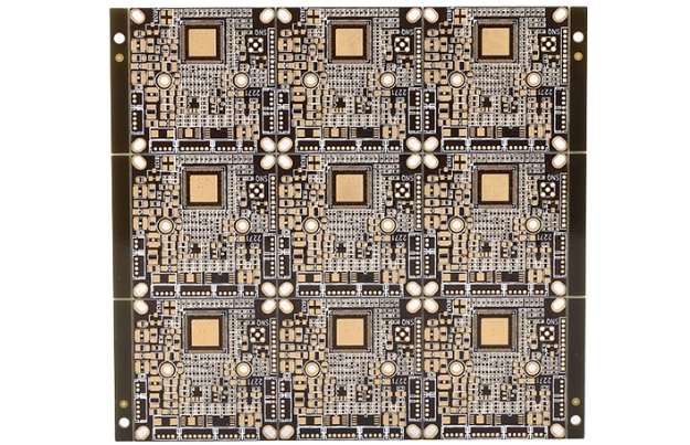
SMTFAB is one reputable 8 layer PCB manufacturer and supplier in China. We have over 12 years of experience in PCB design, fabrication, and PCB assembly service.
8 layer circuit board belongs to multilayer board, typically it has impedance control, blind vias or buried vias. We often use high TG materials to process to 8 layer PCB and the copper thickness is from 1 oz copper to 6 oz copper for inner layers and outer layers.
We are specialized in providing high-quality PCB prototypes to high volume quantities. If you have urgent projects, we can help you to produce a 48H quick-turn service for you.
8 layer printed circuit boards are often used in compact devices that require a limited layout. Due to its complexity and high cost, your 8 layer PCB should be produced by a skilled professional PCB manufacturer.
If you are looking for a reliable 8 layer PCB manufacturer in China, SMTFAB is your perfect choice.
We offer different types of 8 layer PCBs including a flexible circuit board, rigid-flex circuit board, Rogers + FR4 mixed PCB, HDI PCB, and so on.
As the best 8-layer PCB manufacturer, we keep our promise. We make sure you enjoy every bit of our service. Since 2008, SMTFAB has been manufacturing and installing high-quality printed circuit boards. Many customers believe in the quality of our services.
In order to meet different demands for our customers, we have sufficient raw materials in stock, such as Shengyi, KB, Rogers, Nanya, Arlon, Nelco, Isola, MEGTRON 6, and Bergquist.
We have different sales teams to be responsible for different countries, so you don’t need to worry about the communications.

We have passed many certifications like ISO9001, 14000, UL, REACH, and RoHS, so you can guarantee 100% production and reliable service for you.
When you have questions, please email us. We’re always here to support you.
8-Layer PCB: A Complete FAQ Guide
There has been an acute development in the PCB manufacturing industry with the continuous evolution in the electronics industry. For their excellent mechanical and electrical characteristics, 8-layer PCBs have gained widespread usage across various applications. It’s in the interests of anybody designing multilayer PCBs to use eight-layer PCBs.
China’s SMTFAB is among the companies that manufacture PCBs with several layers, namely 8-layer PCBs. This FAQ guide has valuable information for anybody who wants to know more about this PCB stack-up with 8-Layers. Take a glimpse of it.
- What Is An 8-Layer PCB?
- Why Do You Use 8-Layer PCB?
- What Are The Materials Of 8-Layer PCB?
- What Are The Applications Of 8-Layer PCB?
- What Are The 8-Layer PCB Advantages?
- How To Design An 8-Layer PCB?
- What Purposes Should You Fulfill While Designing 8-Layer PCB?
- How Do You Implement An 8-layer PCB Stack-up?
- What Is The 8-Layer PCB stack-up Prototype?
- How Is The Component Arrangement On A Standard 8-Layer PCB?
- How Do You Adjust The Thickness Of 8-Layer PCB?
- What Types Of Surface Finish Do You Use On 8-Layer PCB?
- How Does Solder Mask Affect The Impedance Of 8-Layer PCB stack-up?
- What Vias Do You Use On 8-Layer PCB?
- Why Do You Use The Ground Plane And Power In 8-Layer PCB stack-up?
- What do you need to consider to successfully produce an 8-layer PCB?
- What Do You Look for in Choosing an 8-Layer PCB?
- How Do The 6-Layer And 8-Layer PCBs Differ?
- How Are 8-Layer PCB Pricing Factors Determined?
- How Do You Test 8-Layer PCB?
- How Do You Know Which PCB Manufacturing Company Is The Best One To Choose?
What Is An 8-Layer PCB?
A specific type of multilayer printed circuit board that has 8-Layers of ample routing space is called 8-Layer PCB. The EMC performance is enhanced in this PCB with two added planes. Applications that require multiple power islands use 8-Layer PCB stack-up.

8-Layer PCB
We generally use 8-Layer boards in compact devices like backplanes, wearable watches, motherboards, etc. the board has four layers of wire and four layers of surfaces. Each has seven rows of dielectrics running through it.
8-Layer printed circuit board is a printed board of six layers with a better EMC performance. The board is closed off with a solder mask on the top and bottom.
Why Do You Use 8-Layer PCB?
There are some applications and devices in different industries that need very complex circuits. To make these applications work their best, you need to use an 8-Layer circuit board stack-up. 8-Layer PCBs increase the operating speed of these devices as well as decrease the complex appliances’ sizes.

Highly Functional 8-Layer PCB
To improve signal quality, this PCB uses distinct signal layers separated by power and ground surfaces. The board uses more than four copper layers. This substance improves signal integrity in a variety of board layouts.
The power planes and ground planes on the internal layers also reduce the crosstalk between signal layers. These boards have extra spaces as well. You can fit in other additional components on the board if necessary.
What Are The Materials Of 8-Layer PCB?
Different materials were used for 8-Layer printed circuit board work for other purposes. The type of material determines the device’s performance. Based on the specifics of your device, you should choose the kind of material you’re using in your eight-layer stack.
High-performance printed boards are made of conductive materials and substrates. These are considered to be the best materials for the board production process.
● Substrates
Different substrates like glass-epoxy materials work to insulate signals and heat. High-temperature applications use these substrates for this purpose. These glass-epoxy materials work better to handle the stack-up.
Substrates have great glass transition temperatures. This temperature controls the 8-Layer board stack-up solidness.

8-Layer PCB Materials
● Conductive Materials
The most effective and used conductive material is copper in the fabrication of 8-Layer boards. Copper is a great conductor of heat, reduces heat accumulation in the application, and allows the suitable transfer of signals. That is why it is the perfect option for conductive materials.
Gold and silver are suitable conductive materials too, but they are costly. Copper is an excellent and cheaper option rather than other materials.
What Are The Applications Of 8-Layer PCB?
There is a wide range of applications of 8-Layer PCBs. It is the most used and most common multilayer PCB stack-up. You can find them in most of the appliances.

8-Layer PCB With Immersion Tin
The following are a few popular uses of such a PCB stack-up.
- Medical equipment in the medical industry
- Manufacturing industry
- Automobile or automotive industry
- Aviation industry
- Chemical processing industry
- Space exploration
Many more applications in different industries use 8-Layer PCBs.
What Are The 8-Layer PCB Advantages?
The 8-Layer board has so many advantages in different fields. That is the reason that the use of this PCB is increasing day by day. Various industries nowadays only use this printed board instead of other printed circuit boards.
Some advantages of this board are as follows.
● Increased Functionality
8-Layer PCBs have improved functionalities and speed. They provide way more functionalities to the devices they are applied in. different applications use this board for more reliability and durability.
This printed circuit board has conductive materials on over four layers. These layers of conductive materials increase the signal traces.
● Reduction Of Radiation
High-speed applications may face radiation problems. 8-Layer PCBs can work to get rid of the radiation occurrence in these applications. Unlike other PCB designs, 8-layer designs can remove electromagnetic interference radiation.
● Less Vulnerability
8-Layer PCB used in a device decreases its vulnerability. And it increases the whole performance of the device. This PCB can protect the inner layers from different noises.
As a result, vulnerability to outer forces is reduced.
● Cost-effective
These 8-Layer printed circuit boards are very cost-effective. These boards are very durable and low maintenance. If you want to clean it or replace it, the cost will be reasonable.
How To Design An 8-Layer PCB?
First, it is necessary to choose the kind of stack-up you would like to work with to create the 8-Layer PCB stack-up. A functional design precedes the design process. The whole procedure ensures that you will get the 8-layer stack-up you had wanted.
● Creation Of Idea
The designing process begins with an empty page on the selected designing software. First, you may look for the appropriate way to make sure that your PCB works. You can choose the design software that fulfills all your requirements.
Then you have to develop a schematic, such as the PCB blueprint. You need to add all the information about your PCB stack-up after creating the schematic.

8-Layer PCB Design
● Understanding the arrangement of the stack is a critical step.
● Inclusion Of Component
All details of your required stack-up must be included at the beginning of the designing process. Each little detail is then inked on the schematic.
After that, review everything and make sure everything is alright. Swap any changes in this stage if you want to. You can not change anything once you proceed to the next step.
Define the rules of the design and follow them accordingly in the entire design process. These rules may affect the stack-up primarily. So don’t think of not abiding by them.
● Placement Of Component
Determine where the components of the PCB will be located in this step. Then decide how you want to position the boards’ drill holes and how you want to arrange the layers. Once the route traces are placed on the board, add identifiers and labels to them.
This video gives a solid description of how to construct the stack-up of 8-layer PCB.
What Purposes Should You Fulfill While Designing 8-Layer PCB?
While planning an 8-Layer PCB, you should have some purposes that you want to fulfill in the long run. For that, you have to design very carefully and make sure that you achieve all the objectives of your stack-up design. Some objectives you may want to fulfill while designing the PCB are as follows.
- You should aim at positioning all the signal layers at places close to the planes.
- You must set your goal to lower the impedance. That can be done by adding multiple planes to the PCB stack-up design.
- You have to complete the power and ground planes. Keep an eye on them to couple them as near as possible.
- Your objective should be routing the high-speed signal through the buried layers between the PCB planes.
How Do You Implement An 8-layer PCB Stack-up?
To make an 8-layer stack-up, you’ll need to follow these instructions. It’s critical to follow these to get a board with eight layers, superior performance.
● Alignment Of Ground Planes
If the ground planes are not aligned, they may cause impedance discontinuity. The outer layer components of the PCB must have exceptionally less impedance. Through the vias of the board, the external layer components connect to the inner planes.
● Blind Or Buried Vias
Using buried or blind vias in the PCB stack-up maximizes the available space of the board. This space can be used for component routing. It is essential to arrange blind vias upon the circuit board correctly.

Standard 8-Layer PCB
● Proper Routing Direction
You must figure out the appropriate signal layer numbers for your application. If a PCB contains six signal layers, the signals in the upper and lower levels need to have each layer’s perpendicular guidance to be used. The marks reduce Cross-talk and signaling. They tell users what kind of signals to expect on the printed board.
● Proper Return Path
You have to make a short enough return path to terminate other components’ interaction on the 8-Layer board.
What Is The 8-Layer PCB stack-up Prototype?
When you’re making an 8-layer PCB, you must have a board design ready. The 8-layer stack-up is a basic structure for the other boards to follow.

8-Layer PCB Prototype
The PCB prototype will provide you with the primary testimonial while fabricating other 8-Layer board stack-up. You may run various tests to be sure that the stack-up is functioning right. Then you may proceed with other fabricating procedures.
How Is The Component Arrangement On A Standard 8-Layer PCB?
You have to maintain a proper arrangement of components to fabricate a standard 8-Layer PCB. The exact location of each layer inside the stack-up has to be specified. The layer arrangement should be according to the requirement of your application.
A basic and conventional PCB stack-up design uses these elements in an 8-layer configuration.
- Uppermost layer
- Prepreg
- Ground Plane
- Core
- First inner layer
- Prepreg
- Supply plane
- Core
- Ground surface
- Prepreg
- Interior layer
- Core
- Electrically conductive plane
- Prepreg
- Lower layer

8-Layer PCB’s Component Layout
All the signal layers are isolated by power and ground planes in this component arrangement. The materials you choose for your board affect its impedance. The thickness or dimension of the 8-Layer stack up determines its performance as well.
How Do You Adjust The Thickness Of 8-Layer PCB?
One of the significant factors of an 8-layer PCB is its size. You must consider size while manufacturing your 8-Layer board to get the best outcome.
The thickness of the board has a significant utilized effect on the stack-up performance. We can control the thickness of the materials as the size is considered. sinificnThe following are the methods that you can imply to adjust the thickness of your 8-Layer PCB.
● stack-up Mea Sling
In this procedure, silicone pads are added to the epoxy plates. It controls the pressure balance of the stack-up and removes stack-up measles. It also maintains the thickness uniformity effectively all over the board.

Thickness Of 8-Layer PCB
● Interlayer Offset
Resin recession grooves are applied in the board side design in this process as an alternative to choked flow pads. Hot melting plus dowel and rivet plus can also be utilised depending on the board position.
What Types Of Surface Finish Do You Use On 8-Layer PCB?
The finishing of an 8-layer board’s PCB has a significant influence on its performance. When selecting an 8-Layer board surface finish, it is critical to know what kind would be appropriate for your application.

Different Surface Finishes Of 8-Layer PCB
The right type of surface finish improves the connection between signals of the conducting materials. It will also develop the 8-Layer PCB’s image.
To learn about the options you have for your 8-Layer stack-up, just see the list below.
- Immersion tin (Sn)
- Immersion silver (Au)
- Lead-free HASL or Hot Air Solder Level
- HASL or Hot Air Solder Level
- ENIG
- OSP or Organic Solder Ability Preservative
- ENEPIG
Watch the following video on how you may choose the surface finish for your 8-Layer PCB.
How Does Solder Mask Affect The Impedance Of 8-Layer PCB stack-up?
There is a solder mask on the top layer of every 8-Layer PCB stack-up. And so you can not but calculate the impedance of the PCB stack-up without its effect. It is essential to measure the impact of solder masks on the impedance of an 8-Layer PCB.
The solder mask in a stack-up usually lessens the impedance by sound 2 or 3 ohms. The measurement gets more accurate when there are exceptionally thin traces on the printed circuit board.

Solder Mask Effect On 8-Layer PCB
The effect of solder mask on the impedance of a board decreases when the 8-Layer stack-up thickness is increased. You need to raise the thickness of the materials of the 8-Layer stack-up if you want to lessen the solder mask impedance effect.
What Vias Do You Use On 8-Layer PCB?
To mount the components on an 8-Layer PCB, you require vias on it. The vias settle the connection between different circuit types as well. Some of the vias you can utilise on an 8-Layer stack-up are as follows.
● Buried Vias
In general, buried vias have their shielding included in the layers of PCB stack-up.
● Blind Vias
Using a blind via, you can connect layers on a PCB from the outermost layer to the inside.
● Through-Hole Vias
Through-hole vias start from the top layer of the PCB stack-up and go all the way down to the bottom layer.
● Vias In Pads
On an 8-layer PCB stack-up, you can utilize vias on pads if you’re working with pads.
● Microvans
Microvans are very tiny vias on PCB stack-up that one can not see with empty eyes.

Types Of Vias For 8-Layer PCB
Why Do You Use The Ground Plane And Power In 8-Layer PCB stack-up?
In a layered 8-layer PCB, you may find ground surfaces and power surfaces at various levels. The planes have crucial roles to perform in an 8-Layer board stack-up. It is a must to have these planes on an 8-Layer board for their several functionalities.
Some reasons we use ground planes and power planes in an 8-Layer stack-up are as follows.
● Distribution Of Power
Power planes and ground planes distribute the power of the PCB throughout the board. To distribute low inductance power, these planes play the most critical roles in 8-Layer stack-up.
● Improvement Of Stability
Power planes and ground planes improve the reference voltages’ stability. To stabilize the digital signal exchanging procedure, these two planes come in handy.
● Control Of Crosstalk
A control signal uses power planes as well as ground planes to manage signal crosstalk on an 8-layer board.
What do you need to consider to successfully produce an 8-layer PCB?
The manufacturer needs to consider some factors while manufacturing an 8-Layer PCB to get the best possible outcome. Keeping these factors in mind will also increase the performance of the 8-Layer board. Some of the factors to look out for as you design and produce the PCB are given below.
● Stack-up Measling
The 8-Layer PCB stack-up may have a problem of delamination in the shape of measling. The board’s manufacturing process will be significantly hampered by it. The manufacturer should add pads while compiling the boards together to epoxy plates.
● Bow And Twist
If the printed circuit board contains uneven copper distribution, the board may face the bow and twist problem. You need to design and manufacture the 8-Layer board in the most symmetric way to eliminate this problem.

Manufacturing Process Of 8-Layer PCB
● Material Consistency
The manufacturer should utilize the same materials in fabricating the substrate and core of the 8-Layer stack-up. If different types of materials are used, there may be severe inconsistency problems.
● Core Materials
One difficulty that comes with developing the 8-Layer PCB is that the main ingredients are hard to get. Opt for an available and accessible material for the production of cores of the board. Try not to bring core materials to 8-Layer PCB stack-up.
● Interlayer Offset
The inner layers of an 8-layer stack-up may be offset during fabrication. You need to use rivet dowels or hot melting methods to prevent this problem in printed circuit board sign designs.
What Do You Look for in Choosing an 8-Layer PCB?
You need to consider some essential factors to choose the correct 8-Layer PCB for the best efficiency. The crucial facts that you have to check out to select your 8-Layer stack-up are as follows.
● Signal Layers Coupling
You need to check the coupling of the PCB stack-up. Make sure that the signal layers are tight enough on the adjoining planes.
● Layer Arrangement
Looking at the arrangement of the layers is a crucial step. The single-layer should be close planes here.
It will limit the signal layer’s quantity to the least at every position. Thus there will be a lot of space for the placement of components.
● Signal Return Path
Check if the signals have return paths. The signal return paths should also have another way that will give the inductance a minimum form on the adjacent plane. The return path can be either a ground plane or a power plane.
● Budget
Make sure you are getting the best efficiency as per your budget. To get the best deals, you should have a particular budget. Also, having a specific budget will help you estimate your required materials and how the materials will be used.
How Do The 6-Layer And 8-Layer PCBs Differ?
A 6 layer PCB and an 8-Layer PCB differ in performance, dimensions, etc. there are fewer layers in a 6-Layer stack-up. But you will get additive layers in 8-Layer PCB with added cost.
And so, 8-Layer PCBs cost much more than six-layer PCBs. But 8-Layer PCBs will provide you with more functionalities in comparison to 6 layer PCBs. As the 8-Layer one has more space for component mounting and it can decrease the signal impedance.

6 layer PCB stack-up
An 8-Layer PCB has additional layers that work to solve the electromagnetic interference problem of the application.
How Are 8-Layer PCB Pricing Factors Determined?
The cost of an 8-Layer PCB varies from one to another. Several factors in an 8-Layer stack-up determine its price. The following things play into the pricing of an 8-layer board.
- Board size
- Hole sizes
- Thickness
- Type of surface finish
- Customization determine the board’s accuracy
How Do You Test 8-Layer PCB?
After manufacturing an 8-Layer PCB stack-up, the manufacturer needs to run several tests to determine the board’s accuracy. The tests find out if the board passes all the quality and functional tests.
To test the functionality of the board, the manufacturer runs integrated circuit tests and flying probe tests. To check the quality, the manufacturer conducts tests on the board regarding international quality certifications.

Testing 8-Layer PCB
These tests run the product through several procedures and give different results as per the procedures are conducted. Lastly, the manufacturer compares the results to traditional values. Thus you can determine the accurate performance of your 8-Layer printed circuit boards.
How Do You Know Which PCB Manufacturing Company Is The Best One To Choose?
Choosing the proper manufacturer for 8-Layer PCB is essential. You need to select the perfect manufacturer to get the most efficient 8-Layer boards according to your requirements. You can choose the proper manufacturer by figuring out some specific aspects.
You may check out the following attributes to choose the proper manufacturer of 8-Layer PCBs.
- The manufacturer has proper knowledge of what they are working on.
- The manufacturing company provides customization services according to your application requirement.
- The manufacturing company has experience of the basic requirements.
- The manufacturer uses modern technologies to produce the boards as they are very delicate.
- The manufacturing company has a group of experts of 8-Layer PCB stack-up.
- Your budget copes up with the company’s demand and requirements for the manufacturing process.
- The manufacturer has worked with your specific industry previously.
- If possible, pay a visit to the area of the manufacturing company.
- Make sure that cleanliness and hygiene are maintained during the fabrication process.
- The manufacturing should have the quality and international certificates for 8-Layer PCBs.
Conclusion
The 8-Layer PCB has become way more popular in recent times. A lot of industries use 8-Layer PCB stack-up in their applications. Opting for the best and efficient, durable 8-Layer boards is a must for the better performance of applications.
Whether you want to know more applications or any information about you or us want to take our services, you are welcome to contact us at any time. We will help you with any information and provide you with the best quality 8-Layer PCB according to your unique requirements.
Your Leading 8 Layer PCB Manufacturer in China
As one professional 8 layer PCB supplier in China, we can help you to solve all the issues from quote, order and shipping.
- Over 12 years 8 layer PCB manufacturing experience
- The team supported with over 80 professionals and technical
- On-time delivery with great support from UPS, DHL, and FedEx
- Files receive full CAM review prior to manufacturing
- 48h quick-turn service for your prototype 8 layer PCB
- 7/24 sales and engineering tech support
- Production Facility
- PCB Capabilities
- 8 layer PCB Stackup
| Feature | Capability |
| Quality Grade | Standard IPC 2 and IPC 3 |
| Number of Layers | 2 – 40layers |
| Order Quantity | 1pc – 1Million+pcs |
| Build Time | 24H – 4weeks |
| Material | S1150G, S1165, S1000-2 |
| Board Size | Min 5*5mm | Max 500*650mm |
| Board Thickness | 0.4mm – 6.5mm |
| Copper Weight (Finished) | 0.5oz – 10.0oz |
| Min Tracing/Spacing | 3mil/3mil |
| Solder Mask Sides | As per the file |
| Solder Mask Color | Green, White, Blue, Black, Red, Yellow |
| Silkscreen Sides | As per the file |
| Silkscreen Color | White, Black, Yellow |
| Surface Finish | HASL – Hot Air Solder Leveling |
| Lead-Free HASL – RoHS | |
| ENIG – Electroless Nickle/Immersion Gold – RoHS | |
| Immersion Silver – RoHS | |
| Immersion Tin – RoHS | |
| OSP – Organic Solderability Preservatives – RoHS | |
| Min Annular Ring | 4mil |
| Min Drilling Hole Diameter | 6mil |
| Other Techniques | Gold fingers |
| Blind/Buried Vias |
Please see the details of 8 layer PCB Stack-up as follows:
Releted Some Other PCBs
Why Choose SMTFAB for Your 8 Layer PCB
SMTFAB is one reputable 8 layer PCB manufacturer and supplier in China. We have over 12 years of experience in PCB design, fabrication, and PCB assembly service.
8 layer circuit board belongs to multilayer board, typically it has impedance control, blind vias or buried vias. We often use high TG materials to process to 8 layer PCB and the copper thickness is from 1 oz copper to 6 oz copper for inner layers and outer layers.
We are specialized in providing high-quality PCB prototypes to high volume quantities. If you have urgent projects, we can help you to produce a 48H quick-turn service for you.
8 layer printed circuit boards are often used in compact devices that require a limited layout. Due to its complexity and high cost, your 8 layer PCB should be produced by a skilled professional PCB manufacturer.
If you are looking for a reliable 8 layer PCB manufacturer in China, SMTFAB is your perfect choice.
We offer different types of 8 layer PCBs including a flexible circuit board, rigid-flex circuit board, Rogers + FR4 mixed PCB, HDI PCB, and so on.
As the best 8-layer PCB manufacturer, we keep our promise. We make sure you enjoy every bit of our service. Since 2008, SMTFAB has been manufacturing and installing high-quality printed circuit boards. Many customers believe in the quality of our services.
In order to meet different demands for our customers, we have sufficient raw materials in stock, such as Shengyi, KB, Rogers, Nanya, Arlon, Nelco, Isola, MEGTRON 6, and Bergquist.
We have different sales teams to be responsible for different countries, so you don’t need to worry about the communications.
We have passed many certifications like ISO9001, 14000, UL, REACH, and RoHS, so you can guarantee 100% production and reliable service for you.
When you have questions, please email us. We’re always here to support you.
8-Layer PCB: A Complete FAQ Guide
There has been an acute development in the PCB manufacturing industry with the continuous evolution in the electronics industry. For their excellent mechanical and electrical characteristics, 8-layer PCBs have gained widespread usage across various applications. It’s in the interests of anybody designing multilayer PCBs to use eight-layer PCBs.
China’s SMTFAB is among the companies that manufacture PCBs with several layers, namely 8-layer PCBs. This FAQ guide has valuable information for anybody who wants to know more about this PCB stack-up with 8-Layers. Take a glimpse of it.
- What Is An 8-Layer PCB?
- Why Do You Use 8-Layer PCB?
- What Are The Materials Of 8-Layer PCB?
- What Are The Applications Of 8-Layer PCB?
- What Are The 8-Layer PCB Advantages?
- How To Design An 8-Layer PCB?
- What Purposes Should You Fulfill While Designing 8-Layer PCB?
- How Do You Implement An 8-layer PCB Stack-up?
- What Is The 8-Layer PCB stack-up Prototype?
- How Is The Component Arrangement On A Standard 8-Layer PCB?
- How Do You Adjust The Thickness Of 8-Layer PCB?
- What Types Of Surface Finish Do You Use On 8-Layer PCB?
- How Does Solder Mask Affect The Impedance Of 8-Layer PCB stack-up?
- What Vias Do You Use On 8-Layer PCB?
- Why Do You Use The Ground Plane And Power In 8-Layer PCB stack-up?
- What do you need to consider to successfully produce an 8-layer PCB?
- What Do You Look for in Choosing an 8-Layer PCB?
- How Do The 6-Layer And 8-Layer PCBs Differ?
- How Are 8-Layer PCB Pricing Factors Determined?
- How Do You Test 8-Layer PCB?
- How Do You Know Which PCB Manufacturing Company Is The Best One To Choose?
What Is An 8-Layer PCB?
A specific type of multilayer printed circuit board that has 8-Layers of ample routing space is called 8-Layer PCB. The EMC performance is enhanced in this PCB with two added planes. Applications that require multiple power islands use 8-Layer PCB stack-up.
8-Layer PCB
We generally use 8-Layer boards in compact devices like backplanes, wearable watches, motherboards, etc. the board has four layers of wire and four layers of surfaces. Each has seven rows of dielectrics running through it.
8-Layer printed circuit board is a printed board of six layers with a better EMC performance. The board is closed off with a solder mask on the top and bottom.
Why Do You Use 8-Layer PCB?
There are some applications and devices in different industries that need very complex circuits. To make these applications work their best, you need to use an 8-Layer circuit board stack-up. 8-Layer PCBs increase the operating speed of these devices as well as decrease the complex appliances’ sizes.
Highly Functional 8-Layer PCB
To improve signal quality, this PCB uses distinct signal layers separated by power and ground surfaces. The board uses more than four copper layers. This substance improves signal integrity in a variety of board layouts.
The power planes and ground planes on the internal layers also reduce the crosstalk between signal layers. These boards have extra spaces as well. You can fit in other additional components on the board if necessary.
What Are The Materials Of 8-Layer PCB?
Different materials were used for 8-Layer printed circuit board work for other purposes. The type of material determines the device’s performance. Based on the specifics of your device, you should choose the kind of material you’re using in your eight-layer stack.
High-performance printed boards are made of conductive materials and substrates. These are considered to be the best materials for the board production process.
● Substrates
Different substrates like glass-epoxy materials work to insulate signals and heat. High-temperature applications use these substrates for this purpose. These glass-epoxy materials work better to handle the stack-up.
Substrates have great glass transition temperatures. This temperature controls the 8-Layer board stack-up solidness.
8-Layer PCB Materials
● Conductive Materials
The most effective and used conductive material is copper in the fabrication of 8-Layer boards. Copper is a great conductor of heat, reduces heat accumulation in the application, and allows the suitable transfer of signals. That is why it is the perfect option for conductive materials.
Gold and silver are suitable conductive materials too, but they are costly. Copper is an excellent and cheaper option rather than other materials.
What Are The Applications Of 8-Layer PCB?
There is a wide range of applications of 8-Layer PCBs. It is the most used and most common multilayer PCB stack-up. You can find them in most of the appliances.
8-Layer PCB With Immersion Tin
The following are a few popular uses of such a PCB stack-up.
- Medical equipment in the medical industry
- Manufacturing industry
- Automobile or automotive industry
- Aviation industry
- Chemical processing industry
- Space exploration
Many more applications in different industries use 8-Layer PCBs.
What Are The 8-Layer PCB Advantages?
The 8-Layer board has so many advantages in different fields. That is the reason that the use of this PCB is increasing day by day. Various industries nowadays only use this printed board instead of other printed circuit boards.
Some advantages of this board are as follows.
● Increased Functionality
8-Layer PCBs have improved functionalities and speed. They provide way more functionalities to the devices they are applied in. different applications use this board for more reliability and durability.
This printed circuit board has conductive materials on over four layers. These layers of conductive materials increase the signal traces.
● Reduction Of Radiation
High-speed applications may face radiation problems. 8-Layer PCBs can work to get rid of the radiation occurrence in these applications. Unlike other PCB designs, 8-layer designs can remove electromagnetic interference radiation.
● Less Vulnerability
8-Layer PCB used in a device decreases its vulnerability. And it increases the whole performance of the device. This PCB can protect the inner layers from different noises.
As a result, vulnerability to outer forces is reduced.
● Cost-effective
These 8-Layer printed circuit boards are very cost-effective. These boards are very durable and low maintenance. If you want to clean it or replace it, the cost will be reasonable.
How To Design An 8-Layer PCB?
First, it is necessary to choose the kind of stack-up you would like to work with to create the 8-Layer PCB stack-up. A functional design precedes the design process. The whole procedure ensures that you will get the 8-layer stack-up you had wanted.
● Creation Of Idea
The designing process begins with an empty page on the selected designing software. First, you may look for the appropriate way to make sure that your PCB works. You can choose the design software that fulfills all your requirements.
Then you have to develop a schematic, such as the PCB blueprint. You need to add all the information about your PCB stack-up after creating the schematic.
8-Layer PCB Design
● Understanding the arrangement of the stack is a critical step.
● Inclusion Of Component
All details of your required stack-up must be included at the beginning of the designing process. Each little detail is then inked on the schematic.
After that, review everything and make sure everything is alright. Swap any changes in this stage if you want to. You can not change anything once you proceed to the next step.
Define the rules of the design and follow them accordingly in the entire design process. These rules may affect the stack-up primarily. So don’t think of not abiding by them.
● Placement Of Component
Determine where the components of the PCB will be located in this step. Then decide how you want to position the boards’ drill holes and how you want to arrange the layers. Once the route traces are placed on the board, add identifiers and labels to them.
This video gives a solid description of how to construct the stack-up of 8-layer PCB.
What Purposes Should You Fulfill While Designing 8-Layer PCB?
While planning an 8-Layer PCB, you should have some purposes that you want to fulfill in the long run. For that, you have to design very carefully and make sure that you achieve all the objectives of your stack-up design. Some objectives you may want to fulfill while designing the PCB are as follows.
- You should aim at positioning all the signal layers at places close to the planes.
- You must set your goal to lower the impedance. That can be done by adding multiple planes to the PCB stack-up design.
- You have to complete the power and ground planes. Keep an eye on them to couple them as near as possible.
- Your objective should be routing the high-speed signal through the buried layers between the PCB planes.
How Do You Implement An 8-layer PCB Stack-up?
To make an 8-layer stack-up, you’ll need to follow these instructions. It’s critical to follow these to get a board with eight layers, superior performance.
● Alignment Of Ground Planes
If the ground planes are not aligned, they may cause impedance discontinuity. The outer layer components of the PCB must have exceptionally less impedance. Through the vias of the board, the external layer components connect to the inner planes.
● Blind Or Buried Vias
Using buried or blind vias in the PCB stack-up maximizes the available space of the board. This space can be used for component routing. It is essential to arrange blind vias upon the circuit board correctly.
Standard 8-Layer PCB
● Proper Routing Direction
You must figure out the appropriate signal layer numbers for your application. If a PCB contains six signal layers, the signals in the upper and lower levels need to have each layer’s perpendicular guidance to be used. The marks reduce Cross-talk and signaling. They tell users what kind of signals to expect on the printed board.
● Proper Return Path
You have to make a short enough return path to terminate other components’ interaction on the 8-Layer board.
What Is The 8-Layer PCB stack-up Prototype?
When you’re making an 8-layer PCB, you must have a board design ready. The 8-layer stack-up is a basic structure for the other boards to follow.
8-Layer PCB Prototype
The PCB prototype will provide you with the primary testimonial while fabricating other 8-Layer board stack-up. You may run various tests to be sure that the stack-up is functioning right. Then you may proceed with other fabricating procedures.
How Is The Component Arrangement On A Standard 8-Layer PCB?
You have to maintain a proper arrangement of components to fabricate a standard 8-Layer PCB. The exact location of each layer inside the stack-up has to be specified. The layer arrangement should be according to the requirement of your application.
A basic and conventional PCB stack-up design uses these elements in an 8-layer configuration.
- Uppermost layer
- Prepreg
- Ground Plane
- Core
- First inner layer
- Prepreg
- Supply plane
- Core
- Ground surface
- Prepreg
- Interior layer
- Core
- Electrically conductive plane
- Prepreg
- Lower layer
8-Layer PCB’s Component Layout
All the signal layers are isolated by power and ground planes in this component arrangement. The materials you choose for your board affect its impedance. The thickness or dimension of the 8-Layer stack up determines its performance as well.
How Do You Adjust The Thickness Of 8-Layer PCB?
One of the significant factors of an 8-layer PCB is its size. You must consider size while manufacturing your 8-Layer board to get the best outcome.
The thickness of the board has a significant utilized effect on the stack-up performance. We can control the thickness of the materials as the size is considered. sinificnThe following are the methods that you can imply to adjust the thickness of your 8-Layer PCB.
● stack-up Mea Sling
In this procedure, silicone pads are added to the epoxy plates. It controls the pressure balance of the stack-up and removes stack-up measles. It also maintains the thickness uniformity effectively all over the board.
Thickness Of 8-Layer PCB
● Interlayer Offset
Resin recession grooves are applied in the board side design in this process as an alternative to choked flow pads. Hot melting plus dowel and rivet plus can also be utilised depending on the board position.
What Types Of Surface Finish Do You Use On 8-Layer PCB?
The finishing of an 8-layer board’s PCB has a significant influence on its performance. When selecting an 8-Layer board surface finish, it is critical to know what kind would be appropriate for your application.
Different Surface Finishes Of 8-Layer PCB
The right type of surface finish improves the connection between signals of the conducting materials. It will also develop the 8-Layer PCB’s image.
To learn about the options you have for your 8-Layer stack-up, just see the list below.
- Immersion tin (Sn)
- Immersion silver (Au)
- Lead-free HASL or Hot Air Solder Level
- HASL or Hot Air Solder Level
- ENIG
- OSP or Organic Solder Ability Preservative
- ENEPIG
Watch the following video on how you may choose the surface finish for your 8-Layer PCB.
How Does Solder Mask Affect The Impedance Of 8-Layer PCB stack-up?
There is a solder mask on the top layer of every 8-Layer PCB stack-up. And so you can not but calculate the impedance of the PCB stack-up without its effect. It is essential to measure the impact of solder masks on the impedance of an 8-Layer PCB.
The solder mask in a stack-up usually lessens the impedance by sound 2 or 3 ohms. The measurement gets more accurate when there are exceptionally thin traces on the printed circuit board.
Solder Mask Effect On 8-Layer PCB
The effect of solder mask on the impedance of a board decreases when the 8-Layer stack-up thickness is increased. You need to raise the thickness of the materials of the 8-Layer stack-up if you want to lessen the solder mask impedance effect.
What Vias Do You Use On 8-Layer PCB?
To mount the components on an 8-Layer PCB, you require vias on it. The vias settle the connection between different circuit types as well. Some of the vias you can utilise on an 8-Layer stack-up are as follows.
● Buried Vias
In general, buried vias have their shielding included in the layers of PCB stack-up.
● Blind Vias
Using a blind via, you can connect layers on a PCB from the outermost layer to the inside.
● Through-Hole Vias
Through-hole vias start from the top layer of the PCB stack-up and go all the way down to the bottom layer.
● Vias In Pads
On an 8-layer PCB stack-up, you can utilize vias on pads if you’re working with pads.
● Microvans
Microvans are very tiny vias on PCB stack-up that one can not see with empty eyes.
Types Of Vias For 8-Layer PCB
Why Do You Use The Ground Plane And Power In 8-Layer PCB stack-up?
In a layered 8-layer PCB, you may find ground surfaces and power surfaces at various levels. The planes have crucial roles to perform in an 8-Layer board stack-up. It is a must to have these planes on an 8-Layer board for their several functionalities.
Some reasons we use ground planes and power planes in an 8-Layer stack-up are as follows.
● Distribution Of Power
Power planes and ground planes distribute the power of the PCB throughout the board. To distribute low inductance power, these planes play the most critical roles in 8-Layer stack-up.
● Improvement Of Stability
Power planes and ground planes improve the reference voltages’ stability. To stabilize the digital signal exchanging procedure, these two planes come in handy.
● Control Of Crosstalk
A control signal uses power planes as well as ground planes to manage signal crosstalk on an 8-layer board.
What do you need to consider to successfully produce an 8-layer PCB?
The manufacturer needs to consider some factors while manufacturing an 8-Layer PCB to get the best possible outcome. Keeping these factors in mind will also increase the performance of the 8-Layer board. Some of the factors to look out for as you design and produce the PCB are given below.
● Stack-up Measling
The 8-Layer PCB stack-up may have a problem of delamination in the shape of measling. The board’s manufacturing process will be significantly hampered by it. The manufacturer should add pads while compiling the boards together to epoxy plates.
● Bow And Twist
If the printed circuit board contains uneven copper distribution, the board may face the bow and twist problem. You need to design and manufacture the 8-Layer board in the most symmetric way to eliminate this problem.
Manufacturing Process Of 8-Layer PCB
● Material Consistency
The manufacturer should utilize the same materials in fabricating the substrate and core of the 8-Layer stack-up. If different types of materials are used, there may be severe inconsistency problems.
● Core Materials
One difficulty that comes with developing the 8-Layer PCB is that the main ingredients are hard to get. Opt for an available and accessible material for the production of cores of the board. Try not to bring core materials to 8-Layer PCB stack-up.
● Interlayer Offset
The inner layers of an 8-layer stack-up may be offset during fabrication. You need to use rivet dowels or hot melting methods to prevent this problem in printed circuit board sign designs.
What Do You Look for in Choosing an 8-Layer PCB?
You need to consider some essential factors to choose the correct 8-Layer PCB for the best efficiency. The crucial facts that you have to check out to select your 8-Layer stack-up are as follows.
● Signal Layers Coupling
You need to check the coupling of the PCB stack-up. Make sure that the signal layers are tight enough on the adjoining planes.
● Layer Arrangement
Looking at the arrangement of the layers is a crucial step. The single-layer should be close planes here.
It will limit the signal layer’s quantity to the least at every position. Thus there will be a lot of space for the placement of components.
● Signal Return Path
Check if the signals have return paths. The signal return paths should also have another way that will give the inductance a minimum form on the adjacent plane. The return path can be either a ground plane or a power plane.
● Budget
Make sure you are getting the best efficiency as per your budget. To get the best deals, you should have a particular budget. Also, having a specific budget will help you estimate your required materials and how the materials will be used.
How Do The 6-Layer And 8-Layer PCBs Differ?
A 6 layer PCB and an 8-Layer PCB differ in performance, dimensions, etc. there are fewer layers in a 6-Layer stack-up. But you will get additive layers in 8-Layer PCB with added cost.
And so, 8-Layer PCBs cost much more than six-layer PCBs. But 8-Layer PCBs will provide you with more functionalities in comparison to 6 layer PCBs. As the 8-Layer one has more space for component mounting and it can decrease the signal impedance.
6 layer PCB stack-up
An 8-Layer PCB has additional layers that work to solve the electromagnetic interference problem of the application.
How Are 8-Layer PCB Pricing Factors Determined?
The cost of an 8-Layer PCB varies from one to another. Several factors in an 8-Layer stack-up determine its price. The following things play into the pricing of an 8-layer board.
- Board size
- Hole sizes
- Thickness
- Type of surface finish
- Customization determine the board’s accuracy
How Do You Test 8-Layer PCB?
After manufacturing an 8-Layer PCB stack-up, the manufacturer needs to run several tests to determine the board’s accuracy. The tests find out if the board passes all the quality and functional tests.
To test the functionality of the board, the manufacturer runs integrated circuit tests and flying probe tests. To check the quality, the manufacturer conducts tests on the board regarding international quality certifications.
Testing 8-Layer PCB
These tests run the product through several procedures and give different results as per the procedures are conducted. Lastly, the manufacturer compares the results to traditional values. Thus you can determine the accurate performance of your 8-Layer printed circuit boards.
How Do You Know Which PCB Manufacturing Company Is The Best One To Choose?
Choosing the proper manufacturer for 8-Layer PCB is essential. You need to select the perfect manufacturer to get the most efficient 8-Layer boards according to your requirements. You can choose the proper manufacturer by figuring out some specific aspects.
You may check out the following attributes to choose the proper manufacturer of 8-Layer PCBs.
- The manufacturer has proper knowledge of what they are working on.
- The manufacturing company provides customization services according to your application requirement.
- The manufacturing company has experience of the basic requirements.
- The manufacturer uses modern technologies to produce the boards as they are very delicate.
- The manufacturing company has a group of experts of 8-Layer PCB stack-up.
- Your budget copes up with the company’s demand and requirements for the manufacturing process.
- The manufacturer has worked with your specific industry previously.
- If possible, pay a visit to the area of the manufacturing company.
- Make sure that cleanliness and hygiene are maintained during the fabrication process.
- The manufacturing should have the quality and international certificates for 8-Layer PCBs.
Conclusion
The 8-Layer PCB has become way more popular in recent times. A lot of industries use 8-Layer PCB stack-up in their applications. Opting for the best and efficient, durable 8-Layer boards is a must for the better performance of applications.
Whether you want to know more applications or any information about you or us want to take our services, you are welcome to contact us at any time. We will help you with any information and provide you with the best quality 8-Layer PCB according to your unique requirements.
Your Leading 8 Layer PCB Manufacturer in China
As one professional 8 layer PCB supplier in China, we can help you to solve all the issues from quote, order and shipping.
- Over 12 years 8 layer PCB manufacturing experience
- The team supported with over 80 professionals and technical
- On-time delivery with great support from UPS, DHL, and FedEx
- Files receive full CAM review prior to manufacturing
- 48h quick-turn service for your prototype 8 layer PCB
- 7/24 sales and engineering tech support
Your Leading 8 Layer PCB Manufacturer in China
Your Leading 8 Layer PCB Manufacturer in China
As one professional 8 layer PCB supplier in China, we can help you to solve all the issues from quote, order and shipping.
- Over 12 years 8 layer PCB manufacturing experience
- The team supported with over 80 professionals and technical
- On-time delivery with great support from UPS, DHL, and FedEx
- Files receive full CAM review prior to manufacturing
- 48h quick-turn service for your prototype 8 layer PCB
- 7/24 sales and engineering tech support
- Production Facility
- PCB Capabilities
- 8 layer PCB Stackup
| Feature | Capability |
| Quality Grade | Standard IPC 2 and IPC 3 |
| Number of Layers | 2 – 40layers |
| Order Quantity | 1pc – 1Million+pcs |
| Build Time | 24H – 4weeks |
| Material | S1150G, S1165, S1000-2 |
| Board Size | Min 5*5mm | Max 500*650mm |
| Board Thickness | 0.4mm – 6.5mm |
| Copper Weight (Finished) | 0.5oz – 10.0oz |
| Min Tracing/Spacing | 3mil/3mil |
| Solder Mask Sides | As per the file |
| Solder Mask Color | Green, White, Blue, Black, Red, Yellow |
| Silkscreen Sides | As per the file |
| Silkscreen Color | White, Black, Yellow |
| Surface Finish | HASL – Hot Air Solder Leveling |
| Lead-Free HASL – RoHS | |
| ENIG – Electroless Nickle/Immersion Gold – RoHS | |
| Immersion Silver – RoHS | |
| Immersion Tin – RoHS | |
| OSP – Organic Solderability Preservatives – RoHS | |
| Min Annular Ring | 4mil |
| Min Drilling Hole Diameter | 6mil |
| Other Techniques | Gold fingers |
| Blind/Buried Vias |
Please see the details of 8 layer PCB Stack-up as follows:
- Production Facility
- PCB Capabilities
- 8 layer PCB Stackup
| Feature | Capability |
| Quality Grade | Standard IPC 2 and IPC 3 |
| Number of Layers | 2 – 40layers |
| Order Quantity | 1pc – 1Million+pcs |
| Build Time | 24H – 4weeks |
| Material | S1150G, S1165, S1000-2 |
| Board Size | Min 5*5mm | Max 500*650mm |
| Board Thickness | 0.4mm – 6.5mm |
| Copper Weight (Finished) | 0.5oz – 10.0oz |
| Min Tracing/Spacing | 3mil/3mil |
| Solder Mask Sides | As per the file |
| Solder Mask Color | Green, White, Blue, Black, Red, Yellow |
| Silkscreen Sides | As per the file |
| Silkscreen Color | White, Black, Yellow |
| Surface Finish | HASL – Hot Air Solder Leveling |
| Lead-Free HASL – RoHS | |
| ENIG – Electroless Nickle/Immersion Gold – RoHS | |
| Immersion Silver – RoHS | |
| Immersion Tin – RoHS | |
| OSP – Organic Solderability Preservatives – RoHS | |
| Min Annular Ring | 4mil |
| Min Drilling Hole Diameter | 6mil |
| Other Techniques | Gold fingers |
| Blind/Buried Vias |
Please see the details of 8 layer PCB Stack-up as follows:
Please see the details of 8 layer PCB Stack-up as follows:
Releted Some Other PCBs
Releted Some Other PCBs
Why Choose SMTFAB for Your 8 Layer PCB
SMTFAB is one reputable 8 layer PCB manufacturer and supplier in China. We have over 12 years of experience in PCB design, fabrication, and PCB assembly service.
8 layer circuit board belongs to multilayer board, typically it has impedance control, blind vias or buried vias. We often use high TG materials to process to 8 layer PCB and the copper thickness is from 1 oz copper to 6 oz copper for inner layers and outer layers.
We are specialized in providing high-quality PCB prototypes to high volume quantities. If you have urgent projects, we can help you to produce a 48H quick-turn service for you.
8 layer printed circuit boards are often used in compact devices that require a limited layout. Due to its complexity and high cost, your 8 layer PCB should be produced by a skilled professional PCB manufacturer.
If you are looking for a reliable 8 layer PCB manufacturer in China, SMTFAB is your perfect choice.
We offer different types of 8 layer PCBs including a flexible circuit board, rigid-flex circuit board, Rogers + FR4 mixed PCB, HDI PCB, and so on.
As the best 8-layer PCB manufacturer, we keep our promise. We make sure you enjoy every bit of our service. Since 2008, SMTFAB has been manufacturing and installing high-quality printed circuit boards. Many customers believe in the quality of our services.
In order to meet different demands for our customers, we have sufficient raw materials in stock, such as Shengyi, KB, Rogers, Nanya, Arlon, Nelco, Isola, MEGTRON 6, and Bergquist.
We have different sales teams to be responsible for different countries, so you don’t need to worry about the communications.
We have passed many certifications like ISO9001, 14000, UL, REACH, and RoHS, so you can guarantee 100% production and reliable service for you.
When you have questions, please email us. We’re always here to support you.
8-Layer PCB: A Complete FAQ Guide
There has been an acute development in the PCB manufacturing industry with the continuous evolution in the electronics industry. For their excellent mechanical and electrical characteristics, 8-layer PCBs have gained widespread usage across various applications. It’s in the interests of anybody designing multilayer PCBs to use eight-layer PCBs.
China’s SMTFAB is among the companies that manufacture PCBs with several layers, namely 8-layer PCBs. This FAQ guide has valuable information for anybody who wants to know more about this PCB stack-up with 8-Layers. Take a glimpse of it.
- What Is An 8-Layer PCB?
- Why Do You Use 8-Layer PCB?
- What Are The Materials Of 8-Layer PCB?
- What Are The Applications Of 8-Layer PCB?
- What Are The 8-Layer PCB Advantages?
- How To Design An 8-Layer PCB?
- What Purposes Should You Fulfill While Designing 8-Layer PCB?
- How Do You Implement An 8-layer PCB Stack-up?
- What Is The 8-Layer PCB stack-up Prototype?
- How Is The Component Arrangement On A Standard 8-Layer PCB?
- How Do You Adjust The Thickness Of 8-Layer PCB?
- What Types Of Surface Finish Do You Use On 8-Layer PCB?
- How Does Solder Mask Affect The Impedance Of 8-Layer PCB stack-up?
- What Vias Do You Use On 8-Layer PCB?
- Why Do You Use The Ground Plane And Power In 8-Layer PCB stack-up?
- What do you need to consider to successfully produce an 8-layer PCB?
- What Do You Look for in Choosing an 8-Layer PCB?
- How Do The 6-Layer And 8-Layer PCBs Differ?
- How Are 8-Layer PCB Pricing Factors Determined?
- How Do You Test 8-Layer PCB?
- How Do You Know Which PCB Manufacturing Company Is The Best One To Choose?
What Is An 8-Layer PCB?
A specific type of multilayer printed circuit board that has 8-Layers of ample routing space is called 8-Layer PCB. The EMC performance is enhanced in this PCB with two added planes. Applications that require multiple power islands use 8-Layer PCB stack-up.
8-Layer PCB
We generally use 8-Layer boards in compact devices like backplanes, wearable watches, motherboards, etc. the board has four layers of wire and four layers of surfaces. Each has seven rows of dielectrics running through it.
8-Layer printed circuit board is a printed board of six layers with a better EMC performance. The board is closed off with a solder mask on the top and bottom.
Why Do You Use 8-Layer PCB?
There are some applications and devices in different industries that need very complex circuits. To make these applications work their best, you need to use an 8-Layer circuit board stack-up. 8-Layer PCBs increase the operating speed of these devices as well as decrease the complex appliances’ sizes.
Highly Functional 8-Layer PCB
To improve signal quality, this PCB uses distinct signal layers separated by power and ground surfaces. The board uses more than four copper layers. This substance improves signal integrity in a variety of board layouts.
The power planes and ground planes on the internal layers also reduce the crosstalk between signal layers. These boards have extra spaces as well. You can fit in other additional components on the board if necessary.
What Are The Materials Of 8-Layer PCB?
Different materials were used for 8-Layer printed circuit board work for other purposes. The type of material determines the device’s performance. Based on the specifics of your device, you should choose the kind of material you’re using in your eight-layer stack.
High-performance printed boards are made of conductive materials and substrates. These are considered to be the best materials for the board production process.
● Substrates
Different substrates like glass-epoxy materials work to insulate signals and heat. High-temperature applications use these substrates for this purpose. These glass-epoxy materials work better to handle the stack-up.
Substrates have great glass transition temperatures. This temperature controls the 8-Layer board stack-up solidness.
8-Layer PCB Materials
● Conductive Materials
The most effective and used conductive material is copper in the fabrication of 8-Layer boards. Copper is a great conductor of heat, reduces heat accumulation in the application, and allows the suitable transfer of signals. That is why it is the perfect option for conductive materials.
Gold and silver are suitable conductive materials too, but they are costly. Copper is an excellent and cheaper option rather than other materials.
What Are The Applications Of 8-Layer PCB?
There is a wide range of applications of 8-Layer PCBs. It is the most used and most common multilayer PCB stack-up. You can find them in most of the appliances.
8-Layer PCB With Immersion Tin
The following are a few popular uses of such a PCB stack-up.
- Medical equipment in the medical industry
- Manufacturing industry
- Automobile or automotive industry
- Aviation industry
- Chemical processing industry
- Space exploration
Many more applications in different industries use 8-Layer PCBs.
What Are The 8-Layer PCB Advantages?
The 8-Layer board has so many advantages in different fields. That is the reason that the use of this PCB is increasing day by day. Various industries nowadays only use this printed board instead of other printed circuit boards.
Some advantages of this board are as follows.
● Increased Functionality
8-Layer PCBs have improved functionalities and speed. They provide way more functionalities to the devices they are applied in. different applications use this board for more reliability and durability.
This printed circuit board has conductive materials on over four layers. These layers of conductive materials increase the signal traces.
● Reduction Of Radiation
High-speed applications may face radiation problems. 8-Layer PCBs can work to get rid of the radiation occurrence in these applications. Unlike other PCB designs, 8-layer designs can remove electromagnetic interference radiation.
● Less Vulnerability
8-Layer PCB used in a device decreases its vulnerability. And it increases the whole performance of the device. This PCB can protect the inner layers from different noises.
As a result, vulnerability to outer forces is reduced.
● Cost-effective
These 8-Layer printed circuit boards are very cost-effective. These boards are very durable and low maintenance. If you want to clean it or replace it, the cost will be reasonable.
How To Design An 8-Layer PCB?
First, it is necessary to choose the kind of stack-up you would like to work with to create the 8-Layer PCB stack-up. A functional design precedes the design process. The whole procedure ensures that you will get the 8-layer stack-up you had wanted.
● Creation Of Idea
The designing process begins with an empty page on the selected designing software. First, you may look for the appropriate way to make sure that your PCB works. You can choose the design software that fulfills all your requirements.
Then you have to develop a schematic, such as the PCB blueprint. You need to add all the information about your PCB stack-up after creating the schematic.
8-Layer PCB Design
● Understanding the arrangement of the stack is a critical step.
● Inclusion Of Component
All details of your required stack-up must be included at the beginning of the designing process. Each little detail is then inked on the schematic.
After that, review everything and make sure everything is alright. Swap any changes in this stage if you want to. You can not change anything once you proceed to the next step.
Define the rules of the design and follow them accordingly in the entire design process. These rules may affect the stack-up primarily. So don’t think of not abiding by them.
● Placement Of Component
Determine where the components of the PCB will be located in this step. Then decide how you want to position the boards’ drill holes and how you want to arrange the layers. Once the route traces are placed on the board, add identifiers and labels to them.
This video gives a solid description of how to construct the stack-up of 8-layer PCB.
What Purposes Should You Fulfill While Designing 8-Layer PCB?
While planning an 8-Layer PCB, you should have some purposes that you want to fulfill in the long run. For that, you have to design very carefully and make sure that you achieve all the objectives of your stack-up design. Some objectives you may want to fulfill while designing the PCB are as follows.
- You should aim at positioning all the signal layers at places close to the planes.
- You must set your goal to lower the impedance. That can be done by adding multiple planes to the PCB stack-up design.
- You have to complete the power and ground planes. Keep an eye on them to couple them as near as possible.
- Your objective should be routing the high-speed signal through the buried layers between the PCB planes.
How Do You Implement An 8-layer PCB Stack-up?
To make an 8-layer stack-up, you’ll need to follow these instructions. It’s critical to follow these to get a board with eight layers, superior performance.
● Alignment Of Ground Planes
If the ground planes are not aligned, they may cause impedance discontinuity. The outer layer components of the PCB must have exceptionally less impedance. Through the vias of the board, the external layer components connect to the inner planes.
● Blind Or Buried Vias
Using buried or blind vias in the PCB stack-up maximizes the available space of the board. This space can be used for component routing. It is essential to arrange blind vias upon the circuit board correctly.
Standard 8-Layer PCB
● Proper Routing Direction
You must figure out the appropriate signal layer numbers for your application. If a PCB contains six signal layers, the signals in the upper and lower levels need to have each layer’s perpendicular guidance to be used. The marks reduce Cross-talk and signaling. They tell users what kind of signals to expect on the printed board.
● Proper Return Path
You have to make a short enough return path to terminate other components’ interaction on the 8-Layer board.
What Is The 8-Layer PCB stack-up Prototype?
When you’re making an 8-layer PCB, you must have a board design ready. The 8-layer stack-up is a basic structure for the other boards to follow.
8-Layer PCB Prototype
The PCB prototype will provide you with the primary testimonial while fabricating other 8-Layer board stack-up. You may run various tests to be sure that the stack-up is functioning right. Then you may proceed with other fabricating procedures.
How Is The Component Arrangement On A Standard 8-Layer PCB?
You have to maintain a proper arrangement of components to fabricate a standard 8-Layer PCB. The exact location of each layer inside the stack-up has to be specified. The layer arrangement should be according to the requirement of your application.
A basic and conventional PCB stack-up design uses these elements in an 8-layer configuration.
- Uppermost layer
- Prepreg
- Ground Plane
- Core
- First inner layer
- Prepreg
- Supply plane
- Core
- Ground surface
- Prepreg
- Interior layer
- Core
- Electrically conductive plane
- Prepreg
- Lower layer
8-Layer PCB’s Component Layout
All the signal layers are isolated by power and ground planes in this component arrangement. The materials you choose for your board affect its impedance. The thickness or dimension of the 8-Layer stack up determines its performance as well.
How Do You Adjust The Thickness Of 8-Layer PCB?
One of the significant factors of an 8-layer PCB is its size. You must consider size while manufacturing your 8-Layer board to get the best outcome.
The thickness of the board has a significant utilized effect on the stack-up performance. We can control the thickness of the materials as the size is considered. sinificnThe following are the methods that you can imply to adjust the thickness of your 8-Layer PCB.
● stack-up Mea Sling
In this procedure, silicone pads are added to the epoxy plates. It controls the pressure balance of the stack-up and removes stack-up measles. It also maintains the thickness uniformity effectively all over the board.
Thickness Of 8-Layer PCB
● Interlayer Offset
Resin recession grooves are applied in the board side design in this process as an alternative to choked flow pads. Hot melting plus dowel and rivet plus can also be utilised depending on the board position.
What Types Of Surface Finish Do You Use On 8-Layer PCB?
The finishing of an 8-layer board’s PCB has a significant influence on its performance. When selecting an 8-Layer board surface finish, it is critical to know what kind would be appropriate for your application.
Different Surface Finishes Of 8-Layer PCB
The right type of surface finish improves the connection between signals of the conducting materials. It will also develop the 8-Layer PCB’s image.
To learn about the options you have for your 8-Layer stack-up, just see the list below.
- Immersion tin (Sn)
- Immersion silver (Au)
- Lead-free HASL or Hot Air Solder Level
- HASL or Hot Air Solder Level
- ENIG
- OSP or Organic Solder Ability Preservative
- ENEPIG
Watch the following video on how you may choose the surface finish for your 8-Layer PCB.
How Does Solder Mask Affect The Impedance Of 8-Layer PCB stack-up?
There is a solder mask on the top layer of every 8-Layer PCB stack-up. And so you can not but calculate the impedance of the PCB stack-up without its effect. It is essential to measure the impact of solder masks on the impedance of an 8-Layer PCB.
The solder mask in a stack-up usually lessens the impedance by sound 2 or 3 ohms. The measurement gets more accurate when there are exceptionally thin traces on the printed circuit board.
Solder Mask Effect On 8-Layer PCB
The effect of solder mask on the impedance of a board decreases when the 8-Layer stack-up thickness is increased. You need to raise the thickness of the materials of the 8-Layer stack-up if you want to lessen the solder mask impedance effect.
What Vias Do You Use On 8-Layer PCB?
To mount the components on an 8-Layer PCB, you require vias on it. The vias settle the connection between different circuit types as well. Some of the vias you can utilise on an 8-Layer stack-up are as follows.
● Buried Vias
In general, buried vias have their shielding included in the layers of PCB stack-up.
● Blind Vias
Using a blind via, you can connect layers on a PCB from the outermost layer to the inside.
● Through-Hole Vias
Through-hole vias start from the top layer of the PCB stack-up and go all the way down to the bottom layer.
● Vias In Pads
On an 8-layer PCB stack-up, you can utilize vias on pads if you’re working with pads.
● Microvans
Microvans are very tiny vias on PCB stack-up that one can not see with empty eyes.
Types Of Vias For 8-Layer PCB
Why Do You Use The Ground Plane And Power In 8-Layer PCB stack-up?
In a layered 8-layer PCB, you may find ground surfaces and power surfaces at various levels. The planes have crucial roles to perform in an 8-Layer board stack-up. It is a must to have these planes on an 8-Layer board for their several functionalities.
Some reasons we use ground planes and power planes in an 8-Layer stack-up are as follows.
● Distribution Of Power
Power planes and ground planes distribute the power of the PCB throughout the board. To distribute low inductance power, these planes play the most critical roles in 8-Layer stack-up.
● Improvement Of Stability
Power planes and ground planes improve the reference voltages’ stability. To stabilize the digital signal exchanging procedure, these two planes come in handy.
● Control Of Crosstalk
A control signal uses power planes as well as ground planes to manage signal crosstalk on an 8-layer board.
What do you need to consider to successfully produce an 8-layer PCB?
The manufacturer needs to consider some factors while manufacturing an 8-Layer PCB to get the best possible outcome. Keeping these factors in mind will also increase the performance of the 8-Layer board. Some of the factors to look out for as you design and produce the PCB are given below.
● Stack-up Measling
The 8-Layer PCB stack-up may have a problem of delamination in the shape of measling. The board’s manufacturing process will be significantly hampered by it. The manufacturer should add pads while compiling the boards together to epoxy plates.
● Bow And Twist
If the printed circuit board contains uneven copper distribution, the board may face the bow and twist problem. You need to design and manufacture the 8-Layer board in the most symmetric way to eliminate this problem.
Manufacturing Process Of 8-Layer PCB
● Material Consistency
The manufacturer should utilize the same materials in fabricating the substrate and core of the 8-Layer stack-up. If different types of materials are used, there may be severe inconsistency problems.
● Core Materials
One difficulty that comes with developing the 8-Layer PCB is that the main ingredients are hard to get. Opt for an available and accessible material for the production of cores of the board. Try not to bring core materials to 8-Layer PCB stack-up.
● Interlayer Offset
The inner layers of an 8-layer stack-up may be offset during fabrication. You need to use rivet dowels or hot melting methods to prevent this problem in printed circuit board sign designs.
What Do You Look for in Choosing an 8-Layer PCB?
You need to consider some essential factors to choose the correct 8-Layer PCB for the best efficiency. The crucial facts that you have to check out to select your 8-Layer stack-up are as follows.
● Signal Layers Coupling
You need to check the coupling of the PCB stack-up. Make sure that the signal layers are tight enough on the adjoining planes.
● Layer Arrangement
Looking at the arrangement of the layers is a crucial step. The single-layer should be close planes here.
It will limit the signal layer’s quantity to the least at every position. Thus there will be a lot of space for the placement of components.
● Signal Return Path
Check if the signals have return paths. The signal return paths should also have another way that will give the inductance a minimum form on the adjacent plane. The return path can be either a ground plane or a power plane.
● Budget
Make sure you are getting the best efficiency as per your budget. To get the best deals, you should have a particular budget. Also, having a specific budget will help you estimate your required materials and how the materials will be used.
How Do The 6-Layer And 8-Layer PCBs Differ?
A 6 layer PCB and an 8-Layer PCB differ in performance, dimensions, etc. there are fewer layers in a 6-Layer stack-up. But you will get additive layers in 8-Layer PCB with added cost.
And so, 8-Layer PCBs cost much more than six-layer PCBs. But 8-Layer PCBs will provide you with more functionalities in comparison to 6 layer PCBs. As the 8-Layer one has more space for component mounting and it can decrease the signal impedance.
6 layer PCB stack-up
An 8-Layer PCB has additional layers that work to solve the electromagnetic interference problem of the application.
How Are 8-Layer PCB Pricing Factors Determined?
The cost of an 8-Layer PCB varies from one to another. Several factors in an 8-Layer stack-up determine its price. The following things play into the pricing of an 8-layer board.
- Board size
- Hole sizes
- Thickness
- Type of surface finish
- Customization determine the board’s accuracy
How Do You Test 8-Layer PCB?
After manufacturing an 8-Layer PCB stack-up, the manufacturer needs to run several tests to determine the board’s accuracy. The tests find out if the board passes all the quality and functional tests.
To test the functionality of the board, the manufacturer runs integrated circuit tests and flying probe tests. To check the quality, the manufacturer conducts tests on the board regarding international quality certifications.
Testing 8-Layer PCB
These tests run the product through several procedures and give different results as per the procedures are conducted. Lastly, the manufacturer compares the results to traditional values. Thus you can determine the accurate performance of your 8-Layer printed circuit boards.
How Do You Know Which PCB Manufacturing Company Is The Best One To Choose?
Choosing the proper manufacturer for 8-Layer PCB is essential. You need to select the perfect manufacturer to get the most efficient 8-Layer boards according to your requirements. You can choose the proper manufacturer by figuring out some specific aspects.
You may check out the following attributes to choose the proper manufacturer of 8-Layer PCBs.
- The manufacturer has proper knowledge of what they are working on.
- The manufacturing company provides customization services according to your application requirement.
- The manufacturing company has experience of the basic requirements.
- The manufacturer uses modern technologies to produce the boards as they are very delicate.
- The manufacturing company has a group of experts of 8-Layer PCB stack-up.
- Your budget copes up with the company’s demand and requirements for the manufacturing process.
- The manufacturer has worked with your specific industry previously.
- If possible, pay a visit to the area of the manufacturing company.
- Make sure that cleanliness and hygiene are maintained during the fabrication process.
- The manufacturing should have the quality and international certificates for 8-Layer PCBs.
Conclusion
The 8-Layer PCB has become way more popular in recent times. A lot of industries use 8-Layer PCB stack-up in their applications. Opting for the best and efficient, durable 8-Layer boards is a must for the better performance of applications.
Whether you want to know more applications or any information about you or us want to take our services, you are welcome to contact us at any time. We will help you with any information and provide you with the best quality 8-Layer PCB according to your unique requirements.
Why Choose SMTFAB for Your 8 Layer PCB
SMTFAB is one reputable 8 layer PCB manufacturer and supplier in China. We have over 12 years of experience in PCB design, fabrication, and PCB assembly service.
8 layer circuit board belongs to multilayer board, typically it has impedance control, blind vias or buried vias. We often use high TG materials to process to 8 layer PCB and the copper thickness is from 1 oz copper to 6 oz copper for inner layers and outer layers.
We are specialized in providing high-quality PCB prototypes to high volume quantities. If you have urgent projects, we can help you to produce a 48H quick-turn service for you.
8 layer printed circuit boards are often used in compact devices that require a limited layout. Due to its complexity and high cost, your 8 layer PCB should be produced by a skilled professional PCB manufacturer.
If you are looking for a reliable 8 layer PCB manufacturer in China, SMTFAB is your perfect choice.
We offer different types of 8 layer PCBs including a flexible circuit board, rigid-flex circuit board, Rogers + FR4 mixed PCB, HDI PCB, and so on.
As the best 8-layer PCB manufacturer, we keep our promise. We make sure you enjoy every bit of our service. Since 2008, SMTFAB has been manufacturing and installing high-quality printed circuit boards. Many customers believe in the quality of our services.
In order to meet different demands for our customers, we have sufficient raw materials in stock, such as Shengyi, KB, Rogers, Nanya, Arlon, Nelco, Isola, MEGTRON 6, and Bergquist.
We have different sales teams to be responsible for different countries, so you don’t need to worry about the communications.
We have passed many certifications like ISO9001, 14000, UL, REACH, and RoHS, so you can guarantee 100% production and reliable service for you.
When you have questions, please email us. We’re always here to support you.
8-Layer PCB: A Complete FAQ Guide
There has been an acute development in the PCB manufacturing industry with the continuous evolution in the electronics industry. For their excellent mechanical and electrical characteristics, 8-layer PCBs have gained widespread usage across various applications. It’s in the interests of anybody designing multilayer PCBs to use eight-layer PCBs.
China’s SMTFAB is among the companies that manufacture PCBs with several layers, namely 8-layer PCBs. This FAQ guide has valuable information for anybody who wants to know more about this PCB stack-up with 8-Layers. Take a glimpse of it.
- What Is An 8-Layer PCB?
- Why Do You Use 8-Layer PCB?
- What Are The Materials Of 8-Layer PCB?
- What Are The Applications Of 8-Layer PCB?
- What Are The 8-Layer PCB Advantages?
- How To Design An 8-Layer PCB?
- What Purposes Should You Fulfill While Designing 8-Layer PCB?
- How Do You Implement An 8-layer PCB Stack-up?
- What Is The 8-Layer PCB stack-up Prototype?
- How Is The Component Arrangement On A Standard 8-Layer PCB?
- How Do You Adjust The Thickness Of 8-Layer PCB?
- What Types Of Surface Finish Do You Use On 8-Layer PCB?
- How Does Solder Mask Affect The Impedance Of 8-Layer PCB stack-up?
- What Vias Do You Use On 8-Layer PCB?
- Why Do You Use The Ground Plane And Power In 8-Layer PCB stack-up?
- What do you need to consider to successfully produce an 8-layer PCB?
- What Do You Look for in Choosing an 8-Layer PCB?
- How Do The 6-Layer And 8-Layer PCBs Differ?
- How Are 8-Layer PCB Pricing Factors Determined?
- How Do You Test 8-Layer PCB?
- How Do You Know Which PCB Manufacturing Company Is The Best One To Choose?
What Is An 8-Layer PCB?
A specific type of multilayer printed circuit board that has 8-Layers of ample routing space is called 8-Layer PCB. The EMC performance is enhanced in this PCB with two added planes. Applications that require multiple power islands use 8-Layer PCB stack-up.
We generally use 8-Layer boards in compact devices like backplanes, wearable watches, motherboards, etc. the board has four layers of wire and four layers of surfaces. Each has seven rows of dielectrics running through it.
8-Layer printed circuit board is a printed board of six layers with a better EMC performance. The board is closed off with a solder mask on the top and bottom.
Why Do You Use 8-Layer PCB?
There are some applications and devices in different industries that need very complex circuits. To make these applications work their best, you need to use an 8-Layer circuit board stack-up. 8-Layer PCBs increase the operating speed of these devices as well as decrease the complex appliances’ sizes.
Highly Functional 8-Layer PCB
To improve signal quality, this PCB uses distinct signal layers separated by power and ground surfaces. The board uses more than four copper layers. This substance improves signal integrity in a variety of board layouts.
The power planes and ground planes on the internal layers also reduce the crosstalk between signal layers. These boards have extra spaces as well. You can fit in other additional components on the board if necessary.
What Are The Materials Of 8-Layer PCB?
Different materials were used for 8-Layer printed circuit board work for other purposes. The type of material determines the device’s performance. Based on the specifics of your device, you should choose the kind of material you’re using in your eight-layer stack.
High-performance printed boards are made of conductive materials and substrates. These are considered to be the best materials for the board production process.
Different substrates like glass-epoxy materials work to insulate signals and heat. High-temperature applications use these substrates for this purpose. These glass-epoxy materials work better to handle the stack-up.
Substrates have great glass transition temperatures. This temperature controls the 8-Layer board stack-up solidness.
8-Layer PCB Materials
● Conductive Materials
The most effective and used conductive material is copper in the fabrication of 8-Layer boards. Copper is a great conductor of heat, reduces heat accumulation in the application, and allows the suitable transfer of signals. That is why it is the perfect option for conductive materials.
Gold and silver are suitable conductive materials too, but they are costly. Copper is an excellent and cheaper option rather than other materials.
What Are The Applications Of 8-Layer PCB?
There is a wide range of applications of 8-Layer PCBs. It is the most used and most common multilayer PCB stack-up. You can find them in most of the appliances.
8-Layer PCB With Immersion Tin
The following are a few popular uses of such a PCB stack-up.
- Medical equipment in the medical industry
- Manufacturing industry
- Automobile or automotive industry
- Aviation industry
- Chemical processing industry
- Space exploration
Many more applications in different industries use 8-Layer PCBs.
What Are The 8-Layer PCB Advantages?
The 8-Layer board has so many advantages in different fields. That is the reason that the use of this PCB is increasing day by day. Various industries nowadays only use this printed board instead of other printed circuit boards.
Some advantages of this board are as follows.
● Increased Functionality
8-Layer PCBs have improved functionalities and speed. They provide way more functionalities to the devices they are applied in. different applications use this board for more reliability and durability.
This printed circuit board has conductive materials on over four layers. These layers of conductive materials increase the signal traces.
● Reduction Of Radiation
High-speed applications may face radiation problems. 8-Layer PCBs can work to get rid of the radiation occurrence in these applications. Unlike other PCB designs, 8-layer designs can remove electromagnetic interference radiation.
8-Layer PCB used in a device decreases its vulnerability. And it increases the whole performance of the device. This PCB can protect the inner layers from different noises.
As a result, vulnerability to outer forces is reduced.
These 8-Layer printed circuit boards are very cost-effective. These boards are very durable and low maintenance. If you want to clean it or replace it, the cost will be reasonable.
How To Design An 8-Layer PCB?
First, it is necessary to choose the kind of stack-up you would like to work with to create the 8-Layer PCB stack-up. A functional design precedes the design process. The whole procedure ensures that you will get the 8-layer stack-up you had wanted.
The designing process begins with an empty page on the selected designing software. First, you may look for the appropriate way to make sure that your PCB works. You can choose the design software that fulfills all your requirements.
Then you have to develop a schematic, such as the PCB blueprint. You need to add all the information about your PCB stack-up after creating the schematic.
● Understanding the arrangement of the stack is a critical step.
● Inclusion Of Component
All details of your required stack-up must be included at the beginning of the designing process. Each little detail is then inked on the schematic.
After that, review everything and make sure everything is alright. Swap any changes in this stage if you want to. You can not change anything once you proceed to the next step.
Define the rules of the design and follow them accordingly in the entire design process. These rules may affect the stack-up primarily. So don’t think of not abiding by them.
● Placement Of Component
Determine where the components of the PCB will be located in this step. Then decide how you want to position the boards’ drill holes and how you want to arrange the layers. Once the route traces are placed on the board, add identifiers and labels to them.
This video gives a solid description of how to construct the stack-up of 8-layer PCB.
What Purposes Should You Fulfill While Designing 8-Layer PCB?
While planning an 8-Layer PCB, you should have some purposes that you want to fulfill in the long run. For that, you have to design very carefully and make sure that you achieve all the objectives of your stack-up design. Some objectives you may want to fulfill while designing the PCB are as follows.
- You should aim at positioning all the signal layers at places close to the planes.
- You must set your goal to lower the impedance. That can be done by adding multiple planes to the PCB stack-up design.
- You have to complete the power and ground planes. Keep an eye on them to couple them as near as possible.
- Your objective should be routing the high-speed signal through the buried layers between the PCB planes.
How Do You Implement An 8-layer PCB Stack-up?
To make an 8-layer stack-up, you’ll need to follow these instructions. It’s critical to follow these to get a board with eight layers, superior performance.
● Alignment Of Ground Planes
If the ground planes are not aligned, they may cause impedance discontinuity. The outer layer components of the PCB must have exceptionally less impedance. Through the vias of the board, the external layer components connect to the inner planes.
● Blind Or Buried Vias
Using buried or blind vias in the PCB stack-up maximizes the available space of the board. This space can be used for component routing. It is essential to arrange blind vias upon the circuit board correctly.
● Proper Routing Direction
You must figure out the appropriate signal layer numbers for your application. If a PCB contains six signal layers, the signals in the upper and lower levels need to have each layer’s perpendicular guidance to be used. The marks reduce Cross-talk and signaling. They tell users what kind of signals to expect on the printed board.
You have to make a short enough return path to terminate other components’ interaction on the 8-Layer board.
What Is The 8-Layer PCB stack-up Prototype?
When you’re making an 8-layer PCB, you must have a board design ready. The 8-layer stack-up is a basic structure for the other boards to follow.
8-Layer PCB Prototype
The PCB prototype will provide you with the primary testimonial while fabricating other 8-Layer board stack-up. You may run various tests to be sure that the stack-up is functioning right. Then you may proceed with other fabricating procedures.
How Is The Component Arrangement On A Standard 8-Layer PCB?
You have to maintain a proper arrangement of components to fabricate a standard 8-Layer PCB. The exact location of each layer inside the stack-up has to be specified. The layer arrangement should be according to the requirement of your application.
A basic and conventional PCB stack-up design uses these elements in an 8-layer configuration.
- Uppermost layer
- Prepreg
- Ground Plane
- Core
- First inner layer
- Prepreg
- Supply plane
- Core
- Ground surface
- Prepreg
- Interior layer
- Core
- Electrically conductive plane
- Prepreg
- Lower layer
8-Layer PCB’s Component Layout
All the signal layers are isolated by power and ground planes in this component arrangement. The materials you choose for your board affect its impedance. The thickness or dimension of the 8-Layer stack up determines its performance as well.
How Do You Adjust The Thickness Of 8-Layer PCB?
One of the significant factors of an 8-layer PCB is its size. You must consider size while manufacturing your 8-Layer board to get the best outcome.
The thickness of the board has a significant utilized effect on the stack-up performance. We can control the thickness of the materials as the size is considered. sinificnThe following are the methods that you can imply to adjust the thickness of your 8-Layer PCB.
In this procedure, silicone pads are added to the epoxy plates. It controls the pressure balance of the stack-up and removes stack-up measles. It also maintains the thickness uniformity effectively all over the board.
Thickness Of 8-Layer PCB
Resin recession grooves are applied in the board side design in this process as an alternative to choked flow pads. Hot melting plus dowel and rivet plus can also be utilised depending on the board position.
What Types Of Surface Finish Do You Use On 8-Layer PCB?
The finishing of an 8-layer board’s PCB has a significant influence on its performance. When selecting an 8-Layer board surface finish, it is critical to know what kind would be appropriate for your application.
Different Surface Finishes Of 8-Layer PCB
The right type of surface finish improves the connection between signals of the conducting materials. It will also develop the 8-Layer PCB’s image.
To learn about the options you have for your 8-Layer stack-up, just see the list below.
- Immersion tin (Sn)
- Immersion silver (Au)
- Lead-free HASL or Hot Air Solder Level
- HASL or Hot Air Solder Level
- ENIG
- OSP or Organic Solder Ability Preservative
- ENEPIG
Watch the following video on how you may choose the surface finish for your 8-Layer PCB.
How Does Solder Mask Affect The Impedance Of 8-Layer PCB stack-up?
There is a solder mask on the top layer of every 8-Layer PCB stack-up. And so you can not but calculate the impedance of the PCB stack-up without its effect. It is essential to measure the impact of solder masks on the impedance of an 8-Layer PCB.
The solder mask in a stack-up usually lessens the impedance by sound 2 or 3 ohms. The measurement gets more accurate when there are exceptionally thin traces on the printed circuit board.
Solder Mask Effect On 8-Layer PCB
The effect of solder mask on the impedance of a board decreases when the 8-Layer stack-up thickness is increased. You need to raise the thickness of the materials of the 8-Layer stack-up if you want to lessen the solder mask impedance effect.
What Vias Do You Use On 8-Layer PCB?
To mount the components on an 8-Layer PCB, you require vias on it. The vias settle the connection between different circuit types as well. Some of the vias you can utilise on an 8-Layer stack-up are as follows.
In general, buried vias have their shielding included in the layers of PCB stack-up.
Using a blind via, you can connect layers on a PCB from the outermost layer to the inside.
Through-hole vias start from the top layer of the PCB stack-up and go all the way down to the bottom layer.
On an 8-layer PCB stack-up, you can utilize vias on pads if you’re working with pads.
Microvans are very tiny vias on PCB stack-up that one can not see with empty eyes.
Types Of Vias For 8-Layer PCB
Why Do You Use The Ground Plane And Power In 8-Layer PCB stack-up?
In a layered 8-layer PCB, you may find ground surfaces and power surfaces at various levels. The planes have crucial roles to perform in an 8-Layer board stack-up. It is a must to have these planes on an 8-Layer board for their several functionalities.
Some reasons we use ground planes and power planes in an 8-Layer stack-up are as follows.
● Distribution Of Power
Power planes and ground planes distribute the power of the PCB throughout the board. To distribute low inductance power, these planes play the most critical roles in 8-Layer stack-up.
● Improvement Of Stability
Power planes and ground planes improve the reference voltages’ stability. To stabilize the digital signal exchanging procedure, these two planes come in handy.
● Control Of Crosstalk
A control signal uses power planes as well as ground planes to manage signal crosstalk on an 8-layer board.
What do you need to consider to successfully produce an 8-layer PCB?
The manufacturer needs to consider some factors while manufacturing an 8-Layer PCB to get the best possible outcome. Keeping these factors in mind will also increase the performance of the 8-Layer board. Some of the factors to look out for as you design and produce the PCB are given below.
The 8-Layer PCB stack-up may have a problem of delamination in the shape of measling. The board’s manufacturing process will be significantly hampered by it. The manufacturer should add pads while compiling the boards together to epoxy plates.
If the printed circuit board contains uneven copper distribution, the board may face the bow and twist problem. You need to design and manufacture the 8-Layer board in the most symmetric way to eliminate this problem.
Manufacturing Process Of 8-Layer PCB
● Material Consistency
The manufacturer should utilize the same materials in fabricating the substrate and core of the 8-Layer stack-up. If different types of materials are used, there may be severe inconsistency problems.
One difficulty that comes with developing the 8-Layer PCB is that the main ingredients are hard to get. Opt for an available and accessible material for the production of cores of the board. Try not to bring core materials to 8-Layer PCB stack-up.
The inner layers of an 8-layer stack-up may be offset during fabrication. You need to use rivet dowels or hot melting methods to prevent this problem in printed circuit board sign designs.
What Do You Look for in Choosing an 8-Layer PCB?
You need to consider some essential factors to choose the correct 8-Layer PCB for the best efficiency. The crucial facts that you have to check out to select your 8-Layer stack-up are as follows.
● Signal Layers Coupling
You need to check the coupling of the PCB stack-up. Make sure that the signal layers are tight enough on the adjoining planes.
Looking at the arrangement of the layers is a crucial step. The single-layer should be close planes here.
It will limit the signal layer’s quantity to the least at every position. Thus there will be a lot of space for the placement of components.
Check if the signals have return paths. The signal return paths should also have another way that will give the inductance a minimum form on the adjacent plane. The return path can be either a ground plane or a power plane.
Make sure you are getting the best efficiency as per your budget. To get the best deals, you should have a particular budget. Also, having a specific budget will help you estimate your required materials and how the materials will be used.
How Do The 6-Layer And 8-Layer PCBs Differ?
A 6 layer PCB and an 8-Layer PCB differ in performance, dimensions, etc. there are fewer layers in a 6-Layer stack-up. But you will get additive layers in 8-Layer PCB with added cost.
And so, 8-Layer PCBs cost much more than six-layer PCBs. But 8-Layer PCBs will provide you with more functionalities in comparison to 6 layer PCBs. As the 8-Layer one has more space for component mounting and it can decrease the signal impedance.
An 8-Layer PCB has additional layers that work to solve the electromagnetic interference problem of the application.
How Are 8-Layer PCB Pricing Factors Determined?
The cost of an 8-Layer PCB varies from one to another. Several factors in an 8-Layer stack-up determine its price. The following things play into the pricing of an 8-layer board.
- Board size
- Hole sizes
- Thickness
- Type of surface finish
- Customization determine the board’s accuracy
How Do You Test 8-Layer PCB?
After manufacturing an 8-Layer PCB stack-up, the manufacturer needs to run several tests to determine the board’s accuracy. The tests find out if the board passes all the quality and functional tests.
To test the functionality of the board, the manufacturer runs integrated circuit tests and flying probe tests. To check the quality, the manufacturer conducts tests on the board regarding international quality certifications.
These tests run the product through several procedures and give different results as per the procedures are conducted. Lastly, the manufacturer compares the results to traditional values. Thus you can determine the accurate performance of your 8-Layer printed circuit boards.
How Do You Know Which PCB Manufacturing Company Is The Best One To Choose?
Choosing the proper manufacturer for 8-Layer PCB is essential. You need to select the perfect manufacturer to get the most efficient 8-Layer boards according to your requirements. You can choose the proper manufacturer by figuring out some specific aspects.
You may check out the following attributes to choose the proper manufacturer of 8-Layer PCBs.
- The manufacturer has proper knowledge of what they are working on.
- The manufacturing company provides customization services according to your application requirement.
- The manufacturing company has experience of the basic requirements.
- The manufacturer uses modern technologies to produce the boards as they are very delicate.
- The manufacturing company has a group of experts of 8-Layer PCB stack-up.
- Your budget copes up with the company’s demand and requirements for the manufacturing process.
- The manufacturer has worked with your specific industry previously.
- If possible, pay a visit to the area of the manufacturing company.
- Make sure that cleanliness and hygiene are maintained during the fabrication process.
- The manufacturing should have the quality and international certificates for 8-Layer PCBs.
The 8-Layer PCB has become way more popular in recent times. A lot of industries use 8-Layer PCB stack-up in their applications. Opting for the best and efficient, durable 8-Layer boards is a must for the better performance of applications.
Whether you want to know more applications or any information about you or us want to take our services, you are welcome to contact us at any time. We will help you with any information and provide you with the best quality 8-Layer PCB according to your unique requirements.
Technical Specifications
| 0 | { |
| 1 | " |
| 2 | F |
| 3 | e |
| 4 | a |
| 5 | t |
| 6 | u |
| 7 | r |
| 8 | e |
| 9 | " |
| 10 | : |
| 11 | " |
| 12 | C |
| 13 | a |
| 14 | p |
| 15 | a |
| 16 | b |
| 17 | i |
| 18 | l |
| 19 | i |
| 20 | t |
| 21 | y |
| 22 | " |
| 23 | , |
| 24 | " |
| 25 | Q |
| 26 | u |
| 27 | a |
| 28 | l |
| 29 | i |
| 30 | t |
| 31 | y |
| 32 | |
| 33 | G |
| 34 | r |
| 35 | a |
| 36 | d |
| 37 | e |
| 38 | " |
| 39 | : |
| 40 | " |
| 41 | S |
| 42 | t |
| 43 | a |
| 44 | n |
| 45 | d |
| 46 | a |
| 47 | r |
| 48 | d |
| 49 | |
| 50 | I |
| 51 | P |
| 52 | C |
| 53 | |
| 54 | 2 |
| 55 | |
| 56 | a |
| 57 | n |
| 58 | d |
| 59 | |
| 60 | I |
| 61 | P |
| 62 | C |
| 63 | |
| 64 | 3 |
| 65 | " |
| 66 | , |
| 67 | " |
| 68 | N |
| 69 | u |
| 70 | m |
| 71 | b |
| 72 | e |
| 73 | r |
| 74 | |
| 75 | o |
| 76 | f |
| 77 | |
| 78 | L |
| 79 | a |
| 80 | y |
| 81 | e |
| 82 | r |
| 83 | s |
| 84 | " |
| 85 | : |
| 86 | " |
| 87 | 2 |
| 88 | |
| 89 | – |
| 90 | |
| 91 | 4 |
| 92 | 0 |
| 93 | l |
| 94 | a |
| 95 | y |
| 96 | e |
| 97 | r |
| 98 | s |
| 99 | " |
| 100 | , |
| 101 | " |
| 102 | O |
| 103 | r |
| 104 | d |
| 105 | e |
| 106 | r |
| 107 | |
| 108 | Q |
| 109 | u |
| 110 | a |
| 111 | n |
| 112 | t |
| 113 | i |
| 114 | t |
| 115 | y |
| 116 | " |
| 117 | : |
| 118 | " |
| 119 | 1 |
| 120 | p |
| 121 | c |
| 122 | |
| 123 | – |
| 124 | |
| 125 | 1 |
| 126 | M |
| 127 | i |
| 128 | l |
| 129 | l |
| 130 | i |
| 131 | o |
| 132 | n |
| 133 | + |
| 134 | p |
| 135 | c |
| 136 | s |
| 137 | " |
| 138 | , |
| 139 | " |
| 140 | B |
| 141 | u |
| 142 | i |
| 143 | l |
| 144 | d |
| 145 | |
| 146 | T |
| 147 | i |
| 148 | m |
| 149 | e |
| 150 | " |
| 151 | : |
| 152 | " |
| 153 | 2 |
| 154 | 4 |
| 155 | H |
| 156 | |
| 157 | – |
| 158 | |
| 159 | 4 |
| 160 | w |
| 161 | e |
| 162 | e |
| 163 | k |
| 164 | s |
| 165 | " |
| 166 | , |
| 167 | " |
| 168 | M |
| 169 | a |
| 170 | t |
| 171 | e |
| 172 | r |
| 173 | i |
| 174 | a |
| 175 | l |
| 176 | " |
| 177 | : |
| 178 | " |
| 179 | S |
| 180 | 1 |
| 181 | 1 |
| 182 | 5 |
| 183 | 0 |
| 184 | G |
| 185 | , |
| 186 | |
| 187 | S |
| 188 | 1 |
| 189 | 1 |
| 190 | 6 |
| 191 | 5 |
| 192 | , |
| 193 | |
| 194 | S |
| 195 | 1 |
| 196 | 0 |
| 197 | 0 |
| 198 | 0 |
| 199 | - |
| 200 | 2 |
| 201 | " |
| 202 | , |
| 203 | " |
| 204 | B |
| 205 | o |
| 206 | a |
| 207 | r |
| 208 | d |
| 209 | |
| 210 | S |
| 211 | i |
| 212 | z |
| 213 | e |
| 214 | " |
| 215 | : |
| 216 | " |
| 217 | M |
| 218 | i |
| 219 | n |
| 220 | |
| 221 | 5 |
| 222 | * |
| 223 | 5 |
| 224 | m |
| 225 | m |
| 226 | |
| 227 | | |
| 228 | |
| 229 | M |
| 230 | a |
| 231 | x |
| 232 | |
| 233 | 5 |
| 234 | 0 |
| 235 | 0 |
| 236 | * |
| 237 | 6 |
| 238 | 5 |
| 239 | 0 |
| 240 | m |
| 241 | m |
| 242 | " |
| 243 | , |
| 244 | " |
| 245 | B |
| 246 | o |
| 247 | a |
| 248 | r |
| 249 | d |
| 250 | |
| 251 | T |
| 252 | h |
| 253 | i |
| 254 | c |
| 255 | k |
| 256 | n |
| 257 | e |
| 258 | s |
| 259 | s |
| 260 | " |
| 261 | : |
| 262 | " |
| 263 | 0 |
| 264 | . |
| 265 | 4 |
| 266 | m |
| 267 | m |
| 268 | |
| 269 | – |
| 270 | |
| 271 | 6 |
| 272 | . |
| 273 | 5 |
| 274 | m |
| 275 | m |
| 276 | " |
| 277 | , |
| 278 | " |
| 279 | C |
| 280 | o |
| 281 | p |
| 282 | p |
| 283 | e |
| 284 | r |
| 285 | |
| 286 | W |
| 287 | e |
| 288 | i |
| 289 | g |
| 290 | h |
| 291 | t |
| 292 | |
| 293 | ( |
| 294 | F |
| 295 | i |
| 296 | n |
| 297 | i |
| 298 | s |
| 299 | h |
| 300 | e |
| 301 | d |
| 302 | ) |
| 303 | " |
| 304 | : |
| 305 | " |
| 306 | 0 |
| 307 | . |
| 308 | 5 |
| 309 | o |
| 310 | z |
| 311 | |
| 312 | – |
| 313 | |
| 314 | 1 |
| 315 | 0 |
| 316 | . |
| 317 | 0 |
| 318 | o |
| 319 | z |
| 320 | " |
| 321 | , |
| 322 | " |
| 323 | M |
| 324 | i |
| 325 | n |
| 326 | |
| 327 | T |
| 328 | r |
| 329 | a |
| 330 | c |
| 331 | i |
| 332 | n |
| 333 | g |
| 334 | / |
| 335 | S |
| 336 | p |
| 337 | a |
| 338 | c |
| 339 | i |
| 340 | n |
| 341 | g |
| 342 | " |
| 343 | : |
| 344 | " |
| 345 | 3 |
| 346 | m |
| 347 | i |
| 348 | l |
| 349 | / |
| 350 | 3 |
| 351 | m |
| 352 | i |
| 353 | l |
| 354 | " |
| 355 | , |
| 356 | " |
| 357 | S |
| 358 | o |
| 359 | l |
| 360 | d |
| 361 | e |
| 362 | r |
| 363 | |
| 364 | M |
| 365 | a |
| 366 | s |
| 367 | k |
| 368 | |
| 369 | S |
| 370 | i |
| 371 | d |
| 372 | e |
| 373 | s |
| 374 | " |
| 375 | : |
| 376 | " |
| 377 | A |
| 378 | s |
| 379 | |
| 380 | p |
| 381 | e |
| 382 | r |
| 383 | |
| 384 | t |
| 385 | h |
| 386 | e |
| 387 | |
| 388 | f |
| 389 | i |
| 390 | l |
| 391 | e |
| 392 | " |
| 393 | , |
| 394 | " |
| 395 | S |
| 396 | o |
| 397 | l |
| 398 | d |
| 399 | e |
| 400 | r |
| 401 | |
| 402 | M |
| 403 | a |
| 404 | s |
| 405 | k |
| 406 | |
| 407 | C |
| 408 | o |
| 409 | l |
| 410 | o |
| 411 | r |
| 412 | " |
| 413 | : |
| 414 | " |
| 415 | G |
| 416 | r |
| 417 | e |
| 418 | e |
| 419 | n |
| 420 | , |
| 421 | |
| 422 | W |
| 423 | h |
| 424 | i |
| 425 | t |
| 426 | e |
| 427 | , |
| 428 | |
| 429 | B |
| 430 | l |
| 431 | u |
| 432 | e |
| 433 | , |
| 434 | |
| 435 | B |
| 436 | l |
| 437 | a |
| 438 | c |
| 439 | k |
| 440 | , |
| 441 | |
| 442 | R |
| 443 | e |
| 444 | d |
| 445 | , |
| 446 | |
| 447 | Y |
| 448 | e |
| 449 | l |
| 450 | l |
| 451 | o |
| 452 | w |
| 453 | " |
| 454 | , |
| 455 | " |
| 456 | S |
| 457 | i |
| 458 | l |
| 459 | k |
| 460 | s |
| 461 | c |
| 462 | r |
| 463 | e |
| 464 | e |
| 465 | n |
| 466 | |
| 467 | S |
| 468 | i |
| 469 | d |
| 470 | e |
| 471 | s |
| 472 | " |
| 473 | : |
| 474 | " |
| 475 | A |
| 476 | s |
| 477 | |
| 478 | p |
| 479 | e |
| 480 | r |
| 481 | |
| 482 | t |
| 483 | h |
| 484 | e |
| 485 | |
| 486 | f |
| 487 | i |
| 488 | l |
| 489 | e |
| 490 | " |
| 491 | , |
| 492 | " |
| 493 | S |
| 494 | i |
| 495 | l |
| 496 | k |
| 497 | s |
| 498 | c |
| 499 | r |
| 500 | e |
| 501 | e |
| 502 | n |
| 503 | |
| 504 | C |
| 505 | o |
| 506 | l |
| 507 | o |
| 508 | r |
| 509 | " |
| 510 | : |
| 511 | " |
| 512 | W |
| 513 | h |
| 514 | i |
| 515 | t |
| 516 | e |
| 517 | , |
| 518 | |
| 519 | B |
| 520 | l |
| 521 | a |
| 522 | c |
| 523 | k |
| 524 | , |
| 525 | |
| 526 | Y |
| 527 | e |
| 528 | l |
| 529 | l |
| 530 | o |
| 531 | w |
| 532 | " |
| 533 | , |
| 534 | " |
| 535 | S |
| 536 | u |
| 537 | r |
| 538 | f |
| 539 | a |
| 540 | c |
| 541 | e |
| 542 | |
| 543 | F |
| 544 | i |
| 545 | n |
| 546 | i |
| 547 | s |
| 548 | h |
| 549 | " |
| 550 | : |
| 551 | " |
| 552 | H |
| 553 | A |
| 554 | S |
| 555 | L |
| 556 | |
| 557 | – |
| 558 | |
| 559 | H |
| 560 | o |
| 561 | t |
| 562 | |
| 563 | A |
| 564 | i |
| 565 | r |
| 566 | |
| 567 | S |
| 568 | o |
| 569 | l |
| 570 | d |
| 571 | e |
| 572 | r |
| 573 | |
| 574 | L |
| 575 | e |
| 576 | v |
| 577 | e |
| 578 | l |
| 579 | i |
| 580 | n |
| 581 | g |
| 582 | " |
| 583 | , |
| 584 | " |
| 585 | M |
| 586 | i |
| 587 | n |
| 588 | |
| 589 | A |
| 590 | n |
| 591 | n |
| 592 | u |
| 593 | l |
| 594 | a |
| 595 | r |
| 596 | |
| 597 | R |
| 598 | i |
| 599 | n |
| 600 | g |
| 601 | " |
| 602 | : |
| 603 | " |
| 604 | 4 |
| 605 | m |
| 606 | i |
| 607 | l |
| 608 | " |
| 609 | , |
| 610 | " |
| 611 | M |
| 612 | i |
| 613 | n |
| 614 | |
| 615 | D |
| 616 | r |
| 617 | i |
| 618 | l |
| 619 | l |
| 620 | i |
| 621 | n |
| 622 | g |
| 623 | |
| 624 | H |
| 625 | o |
| 626 | l |
| 627 | e |
| 628 | |
| 629 | D |
| 630 | i |
| 631 | a |
| 632 | m |
| 633 | e |
| 634 | t |
| 635 | e |
| 636 | r |
| 637 | " |
| 638 | : |
| 639 | " |
| 640 | 6 |
| 641 | m |
| 642 | i |
| 643 | l |
| 644 | " |
| 645 | , |
| 646 | " |
| 647 | O |
| 648 | t |
| 649 | h |
| 650 | e |
| 651 | r |
| 652 | |
| 653 | T |
| 654 | e |
| 655 | c |
| 656 | h |
| 657 | n |
| 658 | i |
| 659 | q |
| 660 | u |
| 661 | e |
| 662 | s |
| 663 | " |
| 664 | : |
| 665 | " |
| 666 | G |
| 667 | o |
| 668 | l |
| 669 | d |
| 670 | |
| 671 | f |
| 672 | i |
| 673 | n |
| 674 | g |
| 675 | e |
| 676 | r |
| 677 | s |
| 678 | " |
| 679 | } |
Ready to Get Started?
Contact us today for a custom quote and expert consultation