Your Leading 8 Layer PCB Stackup Manufacturer in China


Your Leading 8 Layer PCB Stackup Manufacturer in China
SMTFAB is a professional 8 layer PCB stackup manufacturer in China, we could provide different types of 8 layer PCB stackup for your project.
- Over 12 years 8 layer PCB stackup design experience
- From 8 layer to 40 layer multilayer PCB
- Certified with UL US and Canada
- 24h quick-turn service for your prototype PCB
- Files receive full CAM review prior to manufacturing
- 7/24 sales and engineering tech support
- Production Facility
- Capabilities


| Feature | Capability |
| Quality Grade | Standard IPC 2 and IPC 3 |
| Number of Layers | 2 – 40layers |
| Order Quantity | 1pc – 1Million+pcs |
| Build Time | 24H – 4weeks |
| Material | S1150G, S1165, S1000-2 |
| Board Size | Min 5*5mm | Max 500*650mm |
| Board Thickness | 0.4mm – 6.5mm |
| Copper Weight (Finished) | 0.5oz – 10.0oz |
| Min Tracing/Spacing | 3mil/3mil |
| Solder Mask Sides | As per the file |
| Solder Mask Color | Green, White, Blue, Black, Red, Yellow |
| Silkscreen Sides | As per the file |
| Silkscreen Color | White, Black, Yellow |
| Surface Finish | HASL – Hot Air Solder Leveling |
| Lead-Free HASL – RoHS | |
| ENIG – Electroless Nickle/Immersion Gold – RoHS | |
| Immersion Silver – RoHS | |
| Immersion Tin – RoHS | |
| OSP – Organic Solderability Preservatives – RoHS | |
| Min Annular Ring | 4mil |
| Min Drilling Hole Diameter | 6mil |
| Other Techniques | Gold fingers |
| Blind/Buried Vias |

Releted Some Other PCBs


Why Choose SMTFAB for Your 8 Layer PCB Stackup
SMTFAB has over 12 years of printed circuit board manufacturing experience, we can offer a wide range of high-quality 8 layer PCB stackup for your projects.
SMTFAB design, layout, and manufacture 8 layer PCB stackup where you need to carefully balance designs around Electro-Magnetic Interference(EMI), frequency, analog, and digital signals, and power planes.
As a reliable 8 layer PCB stackup supplier and manufacturer in China, there are more than 500 workers in our workshop and we have imported much high-tech equipment to meet your complicated 8 layer PCB stackup boards, including 8 layer HDI PCBs, flexible or rigid-flex PCBs.
Obviously the more layers you add to something, the more difficult it becomes. 8 layer PCB stackup is more difficult than 4 layer PCB stack-up or 6 layer PCB stackup.
As an ISO 9001and 14000 certified PCB factory, SMTFAB always puts quality first. When Our engineering team receives your files, they read them very carefully and provide any uncertain issues for your approval prior the manufacturing.
SMTFAB will be one of your best manufacturers for 8 layer PCB stackup demands. We strictly follow the IPC class 2 or class 3 standard of quality.

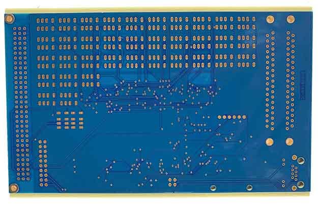
8 layer PCB Stackup
SMTFAB is a valuable PCB fabrication company with a competitive price for 8 layer PCB. You will count on us to provide top quality and deliver in time.
Typically, we recommend you to use High TG (TG170) lamination to produce over 8 layer PCB. Because it’s stable for the PCB stackup.
You will see the specifications from our 8 layer PCB stackup. The board thickness is from 0.4mm to 4.0mm, the copper thickness of the outer layer for 6 layer PCB stackup is from 35um to 420um, and the copper thickness of the inner layer is from 18um to 175um.
Just contact us now when you are ready.
8 Layer PCB Stackup: The Ultimate FAQ Guide
In this guide, you will get information about 8 layer PCB stackup.
Let’s start to read it as follows:
- What Is PCB Stackup?
- What Is 8 Layer PCB StackUp?
- Why You Should Use 8 Layer PCB Stackup?
- What Things You Should Consider While Designing 8 Layer PCB Stackup?
- How Can You Design An 8 Layer Of PCB Stackup?
- In Which Devices 8 Layer PCB Stackup Is Used?
- How Does A Standard 8 Layer PCB Stackup Look Like?
- How Can You Make 8 Layer PCB Stackup Work Well?
- What Are The Techniques For Designing Standard PCB Stack Up?
- What Is The Main Objective When Making 8 Layer PCB Stackup?
- What Components Are Used In 8 Layer PCB Stackup?
- What Is The Conductive Arrangement Of 8 Layers PCB Stack Up?
- How You Can Improve EMC Performance By 8 Layer PCB Stackup?
- What Are The Advantages Of 8 Layer PCB StackUp?
- How Can You Test 8 Layer PCB Stackup?
- Which Top Surfaces You Can Use While Making 8 Layer PCB Stackup?
- What Is The Difference Between 4 Layers And 8 Layer PCB Stackup?
- What Is The Difference Between 6 Layers And 8 Layer PCB Stackup?
- What Laminate Material Is Used In 8 Layer PCB Stackup?
- What Is The Cost Of Designing 8 Layer PCB Stackup?
- How Can You Make 8 Layer PCB Stackup Organization Well?
- How To Choose Manufacturers Of 8 Layer PCB Stackup?
What Is PCB Stackup?
The PCB stack-up is the arrangement of copper layers and insulating layers that makes up a PCB. This PCB stackup is done before designing it.
It depends on the number of signal layers present in the design. The PCB stack-up can increase the electromagnetic capability of the circuit.
Stack-up is an important part of the PCB design and manufacturing process.
A good stack-up design will lead to less electromagnetic emission, poor stack-up will lead to greater electromagnetic emission and greater signal losses.

A Simple PCB stack up
What Is 8 Layer PCB StackUp?
Layer PCB is a layer of firmly stacked layers together. These layers are mutually connected.
It’s used for ample routing for multiple power systems. Each layer of PCB stack-up is prepared under high supervision and great care.
8 layer PCB stackups come in different shapes and sizes. In addition, every variant uses different ingredients for its production.
8 layer PCB stackup is used to improve the EMC performance of the circuit and not to increase the quantity of the routing layers.

8 layer PCB stackup
Why You Should Use 8 Layer PCB Stackup?
Before designing a multilayer PCB, the PCB designer first determines the size of PCB that is required. They also determine the structure of the printed circuit board as well as the requirements of the PCB.
Usually, designers prefer a single or double-layer PCB. The simpler your circuit board design is the lesser are the chances of unnecessary problems.
Usually, an 8 layer PCB stackup is not used very often. However, it has applications on some devices.
The devices having an 8 layer PCB stackup have intact signals. In addition, the designers rely on 8 layer PCB stackup to increase the signal integrity of the circuit board.
Having an 8 layer PCB stackup is one of the most important aspects in achieving the successful configuration of the product.
If the stack up is designed poorly or the material used to make a stack is not of good quality, it would distort the electric performance of the circuit. In addition, it will decrease signal transmission.
It has ground and power planes that help in separating the signals.
What Things You Should Consider While Designing 8 Layer PCB Stackup?
PCB designers can make all kinds of PCB. They can design single, double, or multiple layers of PCB according to the requirement of the customer or requirement of the application.
You have to keep in mind that sometimes you will need to design multiple layer stack up to make such kinds of applications that require intricately printed circuit board.
Before making an 8 layer PCB stack up you need to make sure that the application necessarily requires 8 layers. If it can work with 4 layers or 2 layers, go for lesser layers.
This could be cost-saving. However, it must be considered before designing an 8 layer PCB stackup.
The greater the number of layers the greater are the chances of risks and distortions.
Before you add all the layers, consider using silkscreen layers to identify any component of the printed circuit board.
There should be consistency in the materials you use for 8 layer PCB stackup. You should consider using the same material for the core as well as other components.
Apart from this, the sequence of the layers must be considered before making a stack up.
The spacing between layers, the types, and the numbers of the planes should also be kept in mind.
Try using materials for 8 layers PCB stack up that are easier to manufacture.
How Can You Design An 8 Layer Of PCB Stackup?
Designing a simple layer or double-layer printed circuit board with hundreds of complex components is easier for a PCB designer.
However, designing a PCB consisting of 8 layers is a much complex and delicate matter.
The designers have to face complications and challenges while making it.
The layers of 8 layer PCB stackup are as follow:
- Top layer
- Silkscreen layer
- Solder mask layer
- High-speed signal layer
- Signal layer
- Power lane
- Ground layer
While designing 8 layer PCB stackup it should be kept in mind that the signal layer should be separated from the ground layer or power layer to reduce any electromagnetic emission or distortion.
The arrangement of the layers, their thickness, and the quality of material directly affect the quality of signals and their transmission.

layers of 8 layer PCB stack up
In Which Devices 8 Layer PCB Stackup Is Used?
There are several devices where 8 layer PCB stackup is used.
Following are the applications where 8 layer PCB stackup can be implemented:
- Aviation and naval industries
- Industries that process chemicals
- Production and manufacturing industries
- Medical technology equipment industries
- Automobile industries
- Electrical devices and computer industries
- Space industry
It is a complex PCB and it should be designed only for complicated devices.
The smaller devices usually do not use 8 layer PCB stackup. Rather they use a single-sided, double-layer, or four-layered printed circuit board.

8 layer PCB stack up in electrical devices
How Does A Standard 8 Layer PCB Stackup Look Like?
A standard 8 layer PCB stackup is an 8 PCB board.
It consists of the outer and inner signal layers and has many layers inside of it to prevent signal crosstalk.
There are 7 layers of dielectric that connect four ground planes to four signal layers.

Appearance of 8 layer PCB stack up
How Can You Make 8 Layer PCB Stackup Work Well?
Many factors should be considered before making an 8 layer PCB stack up. One of them is the size of 8 layer PCB stackup.
The thickness of the stack-up directly affects the performance of 8 layer PCB stackup. The thickness can be controlled by controlling the copper thickness.
For 8 layer PCB stackup, the standard thickness is 0.062, 0.093, and 0.125 inches.
Before you start designing your 8 layer PCB stackup, let your PCB designer know your requirements.
The thickness of 8 layer PCB stackup is always based on the thickness of a copper layer, on insulating material, and the top layer of 8 layer PCB stackup.
What Are The Techniques For Designing Standard PCB Stack Up?
There are certain techniques for the standard PCB stack-up design. These should be kept in mind while designing it.
One of the major techniques that should be considered is routing direction.
You may have a different number of layers for your signal layers on the 8 layer PCB stackup.
So, the routing direction of signal traces of different layers of 8 layers PCB stack up must be routed perpendicularly to reduce signal distortion.
Apart from that, a return path for high-speed signals is very important in the case of 8 layer PCB stackup.
It should be kept in mind that the return path should be short. Moreover, they must not interfere with other printed circuit board components.
Another good technique for 8 layer PCB stack-up is that the impedance of outer layer components should be very low. Moreover, the components should have connections to the inner ground plane through vias.
You should also consider increasing the space available for routing of components employing buried vias.
What Is The Main Objective When Making 8 Layer PCB Stackup?
One of the main objectives of 8 layer PCB stackup is good EMC performance. Better EMC performance will lead to better signal integrity.
Certain objectives you should keep in mind when making 8 layer PCB stackup
One of the configurations that include two outer layers of the ground plane can be considered.
With this configuration, all the routing layers are sandwiched with the ground plane and are shielded.
You can also use PCB capacitance technology this would improve high-frequency decoupling.
You should complete ground and power planes. Moreover, connect them as near as possible.
You should consider placing signal layers adjacent to the planes.
The main objective must be considered for the best designing of the 8 layer PCB stackup.
What Components Are Used In 8 Layer PCB Stackup?
An 8 layer PCB stackup is usually made of 6 layers with a top layer and bottom layer. They are usually made of three or more copper foil layers.
These 8 layer PCB stackup to look like several layers of a double-sided circuit board.
All the layers of 8 layer PCB stackup have heat-protective insulation between them. This way the yare laminated to each other.
All the electrical components of the 8 layer PCB stackup are connecting through vias for example through holes, buried, and blind vias.
The 8 layer PCB stackup also contains the ground plane, power plane, and signal plane. These are the essential components of the 8 layers PCB stack up.
The signal layers are separated from each other through the ground plane and power plane.
This arrangement will help in reducing the chances of electromagnetic disruption in 8 layer PCB stackup.
This should be remembered that the arrangement of components, the material of the components being used, and its dimensions directly affect the performance of 8 layer PCB stackup.

Components of 8 layers PCB stackup
What Is The Conductive Arrangement Of 8 Layers PCB Stack Up?
The conductive arrangement of the 8 layers PCB stack-up is the most crucial part for a PCB designer.
Introducing inner layers into 8 layer PCB stackup is a difficult task.
This is the arrangement of 8 layer PCB stackup:
- Top layer- Layer 1 – High-speed signal
- Layer 1 – Ground plane
- Layer 3 – Power plane
- Layer 4- Low-speed signal
- Layer 5 – Ground plane
- Layer 6 – Ground plane
- Layer 7 – Low-speed signal
- Layer 8 – Power plane
- Layer 9 – Ground plane
- Layer 10 – High-speed signal
- Bottom layer
This arrangement has a huge effect on the working of 8 layer PCB stackup.
As you can see, the top and bottom layers have a ground plane and inner layer sandwiched between them, this would reduce Electromagnetic interference and signal distortion.
How You Can Improve EMC Performance By 8 Layer PCB Stackup?
One of the major roles of the 8 layers PCB stack-up is better EMC performance by adding two more planes between the two peripheral signal layers.
The lesser is the electromagnetic emission from the circuit, the lesser would be distortions in the signals and good signal integrity.
However, this feature adds cost to the 8 layer PCB stackup. The betters are the EMC performance of the circuit, the better and more costly is the 8 layer PCB stackup.

Conductive arrangement of 8 layers PCB stack up
What Are The Advantages Of 8 Layer PCB StackUp?
8 layer PCB stackup is the modern electronic which has many advantages.
Good EMC performance. Lesser Electromagnetic interference.
Although they are complex in structure they have extremely good quality and function. This 8 layer PCB stackup has more space for its components as compare to other PCBs.
These 8 layer PCB stackup decrease the vulnerability of the PCB. Since all the inner layers are protected from any external forces or distortion.
Apart from them they have increased functionality and speed up the device functioning.
The 8 layer PCB stackup is highly reliable.
Although the cost of 8 layer PCB stackup is greater than any other PCB it is an advantage. 8 layer PCB stackup would require a lot less money for cleaning and replacement. They usually require a lot less replacement.
They are highly durable.
Usually, in high-speed devices, there are chances of radiation. However, in 8 layer PCB stackup there is no radiation emission
How Can You Test 8 Layer PCB Stackup?
To check the proper working and function of the 8 layer PCB stackup different tests are performed.
They can either be quality assurance tests or functional tests.
To check the function of 8 layer PCB stackup flying probe testis performed.
Another option is an integrated circuit test.
Apart from that micro functioning test can also be performed.
There is another test known as the PCB contamination test. It is performed to make sure there is not any contamination in the circuit board that can cause corrosion of the circuit board.
In the case of quality tests, different international quality certification tests are performed.
In this way, an 8 layer PCB stackup functioning is tested.
Which Top Surfaces You Can Use While Making 8 Layer PCB Stackup?
The top layer of the 8 layer PCB stackup is very important. As it plays an important role in the physical appearance of stack up.
In addition, the top layer helps in improving the signal connection of the conducting material of the 8 layer PCB stackup.
There are many kinds of surface finishes for 8 layer PCB stackup that you can use. These are
- Immersion Silver top layer
- Immersion Tin top layer
- Organic Solder Ability Level top layer
- Electroless Nickel Electroless Palladium Immersion gold top layer
- Hot Air Solder Level top layer
- Electroless Nickel Immersion Gold top layer
All these surfaces are of greater quality and affect significantly the working of 8 layer PCB stackup.
What Is The Difference Between 4 Layers And 8 Layer PCB Stackup?
There are many differences between the 4 layers PCB and 8 layer PCB stackup.
4 layers of PCB stackup are made of 4 layers of fiberglass.
These layers are Top layer, VCC, GND, and Bottom layer.
4 layers PCB has few advantages over the double-sided circuit board. 4 layers PCB stackup is easier to the layout.
They are much more compact than 8 layer PCB stackup and have greater repulsion to noise than 8 layer PCB stackup.
Whereas 8 layer PCB is made up of 6 layers along with the top and bottom layer.
8 layer PCB stackup has greater EMC performance and thus is more costly than 4 layers PCB stack up.
What Is The Difference Between 6 Layers And 8 Layer PCB Stackup?
You can find many differences between 6 layers and 8 layer PCB stackup.
6 layers PCB consists of a total of 6 layers including the top and bottom layer.
The configuration of 6 layers PCB stackup are as follow:
- Top layer
- Inner signal
- Ground plane
- Power plane
- Inner signal
- Bottom signal
This is the configuration of 8 layer PCB stackup.
Whereas the 8 layer PCB stackup configuration is quite different from it.
In performance, the 8 layer PCB stackup is much more good than the 6 layers PCB stack up.
However, 8 layers PCB stack-up has a greater cost than 6 layer PCB stack-up.
With increasing inner layers, there is an increase in the cost of the PCB circuit.
8 layer PCB stackup also has greater EMC performance than 6 layer PCB stackup.
What Laminate Material Is Used In 8 Layer PCB Stackup?
Choosing a good laminate material while designing 8 layer PCB stackup is really important.
Since the laminating material helps in the coupling of different layers of 8 layers PCB stack up.
If the coupling is done right the performance of 8 layer PCB stackup would be excellent.
In addition, if the quality of laminate material is not good and it does not couple layers well, it would result in diminished performance.
The recommended laminate material for 8 layer PCB stackup is Tg170 laminate material. This laminate help to avoid any quality problem during your PCB assembly for example delamination and blister in the lead-free assembly process.
So selection of laminate material is also crucial in determining the quality of 8 layer PCB stackup.

Laminate material for 8 layers PCB stack up
What Is The Cost Of Designing 8 Layer PCB Stackup?
The cost of the 8 layer PCB stackup is another important factor that must be considered.
The cost of a PCB circuit depends on the material and design of the PCB circuit.
However, the making of an 8 layer PCB stackup re-quire extreme intricacy delicacy, and precision.
If you are making a PCB circuit board of single, double, or 4 layers PCBs, then it would cost lower than an 8 layer PCB stackup.
Since the 8 layer PCB stackup has a greater number of inner delicate layers that are costly yet more efficient.
If you are making PCB for a normal routine device it would be less costly and if you are making an 8 layer PCB stackup for a high-tech device then it would be expensive.
How Can You Make 8 Layer PCB Stackup Organization Well?
PCB technology has changed over the period. It has become advanced and demanding.
PCBs have changed from two layers to 4 layers to multiple layered PCB boards.
However, with the increasing layers, the capability, and function of PCBs increase.
The required number of layers of PCBs depends on the type of application, operating frequency, pin density, etc
In the case of 4 layer PCB, there is a top layer and bottom layer that act as signal layers. Layer 2 and layer 3 serves as the planes
In 8 layer PCB stackup, there are seven layers of dielectric that bond four plane layers and four signal layers.

Well organization of 8 layer PCB stack up
How To Choose Manufacturers Of 8 Layer PCB Stackup?
Wisely choosing a good 8 layer PCB stackup manufacturer is really important.
SMTFAB is a professional and excellent 8 layer PCB stackup manufacturer and supplier.
It is mostly used in devices that need strict spacing. SMTFAB provides the best quality of 8 layer PCB stackup.
The good layering done by PCB manufacturers in 8 layer PCB stackup helps to improve the EMC performance.
SMTFAB provides high-quality 8 layer PCB stackup board products and PCB assembly service to more than 3000 customers around the world.
SMTFAB are certified by many international certifications like ISO9001 quality system certification, ISO 14001 environmental system certification.
Your Leading 8 Layer PCB Stackup Manufacturer in China
SMTFAB is a professional 8 layer PCB stackup manufacturer in China, we could provide different types of 8 layer PCB stackup for your project.
- Over 12 years 8 layer PCB stackup design experience
- From 8 layer to 40 layer multilayer PCB
- Certified with UL US and Canada
- 24h quick-turn service for your prototype PCB
- Files receive full CAM review prior to manufacturing
- 7/24 sales and engineering tech support
- Production Facility
- Capabilities
| Feature | Capability |
| Quality Grade | Standard IPC 2 and IPC 3 |
| Number of Layers | 2 – 40layers |
| Order Quantity | 1pc – 1Million+pcs |
| Build Time | 24H – 4weeks |
| Material | S1150G, S1165, S1000-2 |
| Board Size | Min 5*5mm | Max 500*650mm |
| Board Thickness | 0.4mm – 6.5mm |
| Copper Weight (Finished) | 0.5oz – 10.0oz |
| Min Tracing/Spacing | 3mil/3mil |
| Solder Mask Sides | As per the file |
| Solder Mask Color | Green, White, Blue, Black, Red, Yellow |
| Silkscreen Sides | As per the file |
| Silkscreen Color | White, Black, Yellow |
| Surface Finish | HASL – Hot Air Solder Leveling |
| Lead-Free HASL – RoHS | |
| ENIG – Electroless Nickle/Immersion Gold – RoHS | |
| Immersion Silver – RoHS | |
| Immersion Tin – RoHS | |
| OSP – Organic Solderability Preservatives – RoHS | |
| Min Annular Ring | 4mil |
| Min Drilling Hole Diameter | 6mil |
| Other Techniques | Gold fingers |
| Blind/Buried Vias |
Releted Some Other PCBs
Why Choose SMTFAB for Your 8 Layer PCB Stackup
SMTFAB has over 12 years of printed circuit board manufacturing experience, we can offer a wide range of high-quality 8 layer PCB stackup for your projects.
SMTFAB design, layout, and manufacture 8 layer PCB stackup where you need to carefully balance designs around Electro-Magnetic Interference(EMI), frequency, analog, and digital signals, and power planes.
As a reliable 8 layer PCB stackup supplier and manufacturer in China, there are more than 500 workers in our workshop and we have imported much high-tech equipment to meet your complicated 8 layer PCB stackup boards, including 8 layer HDI PCBs, flexible or rigid-flex PCBs.
Obviously the more layers you add to something, the more difficult it becomes. 8 layer PCB stackup is more difficult than 4 layer PCB stack-up or 6 layer PCB stackup.
As an ISO 9001and 14000 certified PCB factory, SMTFAB always puts quality first. When Our engineering team receives your files, they read them very carefully and provide any uncertain issues for your approval prior the manufacturing.
SMTFAB will be one of your best manufacturers for 8 layer PCB stackup demands. We strictly follow the IPC class 2 or class 3 standard of quality.
8 layer PCB Stackup
SMTFAB is a valuable PCB fabrication company with a competitive price for 8 layer PCB. You will count on us to provide top quality and deliver in time.
Typically, we recommend you to use High TG (TG170) lamination to produce over 8 layer PCB. Because it’s stable for the PCB stackup.
You will see the specifications from our 8 layer PCB stackup. The board thickness is from 0.4mm to 4.0mm, the copper thickness of the outer layer for 6 layer PCB stackup is from 35um to 420um, and the copper thickness of the inner layer is from 18um to 175um.
Just contact us now when you are ready.
8 Layer PCB Stackup: The Ultimate FAQ Guide
In this guide, you will get information about 8 layer PCB stackup.
Let’s start to read it as follows:
- What Is PCB Stackup?
- What Is 8 Layer PCB StackUp?
- Why You Should Use 8 Layer PCB Stackup?
- What Things You Should Consider While Designing 8 Layer PCB Stackup?
- How Can You Design An 8 Layer Of PCB Stackup?
- In Which Devices 8 Layer PCB Stackup Is Used?
- How Does A Standard 8 Layer PCB Stackup Look Like?
- How Can You Make 8 Layer PCB Stackup Work Well?
- What Are The Techniques For Designing Standard PCB Stack Up?
- What Is The Main Objective When Making 8 Layer PCB Stackup?
- What Components Are Used In 8 Layer PCB Stackup?
- What Is The Conductive Arrangement Of 8 Layers PCB Stack Up?
- How You Can Improve EMC Performance By 8 Layer PCB Stackup?
- What Are The Advantages Of 8 Layer PCB StackUp?
- How Can You Test 8 Layer PCB Stackup?
- Which Top Surfaces You Can Use While Making 8 Layer PCB Stackup?
- What Is The Difference Between 4 Layers And 8 Layer PCB Stackup?
- What Is The Difference Between 6 Layers And 8 Layer PCB Stackup?
- What Laminate Material Is Used In 8 Layer PCB Stackup?
- What Is The Cost Of Designing 8 Layer PCB Stackup?
- How Can You Make 8 Layer PCB Stackup Organization Well?
- How To Choose Manufacturers Of 8 Layer PCB Stackup?
What Is PCB Stackup?
The PCB stack-up is the arrangement of copper layers and insulating layers that makes up a PCB. This PCB stackup is done before designing it.
It depends on the number of signal layers present in the design. The PCB stack-up can increase the electromagnetic capability of the circuit.
Stack-up is an important part of the PCB design and manufacturing process.
A good stack-up design will lead to less electromagnetic emission, poor stack-up will lead to greater electromagnetic emission and greater signal losses.
A Simple PCB stack up
What Is 8 Layer PCB StackUp?
Layer PCB is a layer of firmly stacked layers together. These layers are mutually connected.
It’s used for ample routing for multiple power systems. Each layer of PCB stack-up is prepared under high supervision and great care.
8 layer PCB stackups come in different shapes and sizes. In addition, every variant uses different ingredients for its production.
8 layer PCB stackup is used to improve the EMC performance of the circuit and not to increase the quantity of the routing layers.
8 layer PCB stackup
Why You Should Use 8 Layer PCB Stackup?
Before designing a multilayer PCB, the PCB designer first determines the size of PCB that is required. They also determine the structure of the printed circuit board as well as the requirements of the PCB.
Usually, designers prefer a single or double-layer PCB. The simpler your circuit board design is the lesser are the chances of unnecessary problems.
Usually, an 8 layer PCB stackup is not used very often. However, it has applications on some devices.
The devices having an 8 layer PCB stackup have intact signals. In addition, the designers rely on 8 layer PCB stackup to increase the signal integrity of the circuit board.
Having an 8 layer PCB stackup is one of the most important aspects in achieving the successful configuration of the product.
If the stack up is designed poorly or the material used to make a stack is not of good quality, it would distort the electric performance of the circuit. In addition, it will decrease signal transmission.
It has ground and power planes that help in separating the signals.
What Things You Should Consider While Designing 8 Layer PCB Stackup?
PCB designers can make all kinds of PCB. They can design single, double, or multiple layers of PCB according to the requirement of the customer or requirement of the application.
You have to keep in mind that sometimes you will need to design multiple layer stack up to make such kinds of applications that require intricately printed circuit board.
Before making an 8 layer PCB stack up you need to make sure that the application necessarily requires 8 layers. If it can work with 4 layers or 2 layers, go for lesser layers.
This could be cost-saving. However, it must be considered before designing an 8 layer PCB stackup.
The greater the number of layers the greater are the chances of risks and distortions.
Before you add all the layers, consider using silkscreen layers to identify any component of the printed circuit board.
There should be consistency in the materials you use for 8 layer PCB stackup. You should consider using the same material for the core as well as other components.
Apart from this, the sequence of the layers must be considered before making a stack up.
The spacing between layers, the types, and the numbers of the planes should also be kept in mind.
Try using materials for 8 layers PCB stack up that are easier to manufacture.
How Can You Design An 8 Layer Of PCB Stackup?
Designing a simple layer or double-layer printed circuit board with hundreds of complex components is easier for a PCB designer.
However, designing a PCB consisting of 8 layers is a much complex and delicate matter.
The designers have to face complications and challenges while making it.
The layers of 8 layer PCB stackup are as follow:
- Top layer
- Silkscreen layer
- Solder mask layer
- High-speed signal layer
- Signal layer
- Power lane
- Ground layer
While designing 8 layer PCB stackup it should be kept in mind that the signal layer should be separated from the ground layer or power layer to reduce any electromagnetic emission or distortion.
The arrangement of the layers, their thickness, and the quality of material directly affect the quality of signals and their transmission.
layers of 8 layer PCB stack up
In Which Devices 8 Layer PCB Stackup Is Used?
There are several devices where 8 layer PCB stackup is used.
Following are the applications where 8 layer PCB stackup can be implemented:
- Aviation and naval industries
- Industries that process chemicals
- Production and manufacturing industries
- Medical technology equipment industries
- Automobile industries
- Electrical devices and computer industries
- Space industry
It is a complex PCB and it should be designed only for complicated devices.
The smaller devices usually do not use 8 layer PCB stackup. Rather they use a single-sided, double-layer, or four-layered printed circuit board.
8 layer PCB stack up in electrical devices
How Does A Standard 8 Layer PCB Stackup Look Like?
A standard 8 layer PCB stackup is an 8 PCB board.
It consists of the outer and inner signal layers and has many layers inside of it to prevent signal crosstalk.
There are 7 layers of dielectric that connect four ground planes to four signal layers.
Appearance of 8 layer PCB stack up
How Can You Make 8 Layer PCB Stackup Work Well?
Many factors should be considered before making an 8 layer PCB stack up. One of them is the size of 8 layer PCB stackup.
The thickness of the stack-up directly affects the performance of 8 layer PCB stackup. The thickness can be controlled by controlling the copper thickness.
For 8 layer PCB stackup, the standard thickness is 0.062, 0.093, and 0.125 inches.
Before you start designing your 8 layer PCB stackup, let your PCB designer know your requirements.
The thickness of 8 layer PCB stackup is always based on the thickness of a copper layer, on insulating material, and the top layer of 8 layer PCB stackup.
What Are The Techniques For Designing Standard PCB Stack Up?
There are certain techniques for the standard PCB stack-up design. These should be kept in mind while designing it.
One of the major techniques that should be considered is routing direction.
You may have a different number of layers for your signal layers on the 8 layer PCB stackup.
So, the routing direction of signal traces of different layers of 8 layers PCB stack up must be routed perpendicularly to reduce signal distortion.
Apart from that, a return path for high-speed signals is very important in the case of 8 layer PCB stackup.
It should be kept in mind that the return path should be short. Moreover, they must not interfere with other printed circuit board components.
Another good technique for 8 layer PCB stack-up is that the impedance of outer layer components should be very low. Moreover, the components should have connections to the inner ground plane through vias.
You should also consider increasing the space available for routing of components employing buried vias.
What Is The Main Objective When Making 8 Layer PCB Stackup?
One of the main objectives of 8 layer PCB stackup is good EMC performance. Better EMC performance will lead to better signal integrity.
Certain objectives you should keep in mind when making 8 layer PCB stackup
One of the configurations that include two outer layers of the ground plane can be considered.
With this configuration, all the routing layers are sandwiched with the ground plane and are shielded.
You can also use PCB capacitance technology this would improve high-frequency decoupling.
You should complete ground and power planes. Moreover, connect them as near as possible.
You should consider placing signal layers adjacent to the planes.
The main objective must be considered for the best designing of the 8 layer PCB stackup.
What Components Are Used In 8 Layer PCB Stackup?
An 8 layer PCB stackup is usually made of 6 layers with a top layer and bottom layer. They are usually made of three or more copper foil layers.
These 8 layer PCB stackup to look like several layers of a double-sided circuit board.
All the layers of 8 layer PCB stackup have heat-protective insulation between them. This way the yare laminated to each other.
All the electrical components of the 8 layer PCB stackup are connecting through vias for example through holes, buried, and blind vias.
The 8 layer PCB stackup also contains the ground plane, power plane, and signal plane. These are the essential components of the 8 layers PCB stack up.
The signal layers are separated from each other through the ground plane and power plane.
This arrangement will help in reducing the chances of electromagnetic disruption in 8 layer PCB stackup.
This should be remembered that the arrangement of components, the material of the components being used, and its dimensions directly affect the performance of 8 layer PCB stackup.
Components of 8 layers PCB stackup
What Is The Conductive Arrangement Of 8 Layers PCB Stack Up?
The conductive arrangement of the 8 layers PCB stack-up is the most crucial part for a PCB designer.
Introducing inner layers into 8 layer PCB stackup is a difficult task.
This is the arrangement of 8 layer PCB stackup:
- Top layer- Layer 1 – High-speed signal
- Layer 1 – Ground plane
- Layer 3 – Power plane
- Layer 4- Low-speed signal
- Layer 5 – Ground plane
- Layer 6 – Ground plane
- Layer 7 – Low-speed signal
- Layer 8 – Power plane
- Layer 9 – Ground plane
- Layer 10 – High-speed signal
- Bottom layer
This arrangement has a huge effect on the working of 8 layer PCB stackup.
As you can see, the top and bottom layers have a ground plane and inner layer sandwiched between them, this would reduce Electromagnetic interference and signal distortion.
How You Can Improve EMC Performance By 8 Layer PCB Stackup?
One of the major roles of the 8 layers PCB stack-up is better EMC performance by adding two more planes between the two peripheral signal layers.
The lesser is the electromagnetic emission from the circuit, the lesser would be distortions in the signals and good signal integrity.
However, this feature adds cost to the 8 layer PCB stackup. The betters are the EMC performance of the circuit, the better and more costly is the 8 layer PCB stackup.
Conductive arrangement of 8 layers PCB stack up
What Are The Advantages Of 8 Layer PCB StackUp?
8 layer PCB stackup is the modern electronic which has many advantages.
Good EMC performance. Lesser Electromagnetic interference.
Although they are complex in structure they have extremely good quality and function. This 8 layer PCB stackup has more space for its components as compare to other PCBs.
These 8 layer PCB stackup decrease the vulnerability of the PCB. Since all the inner layers are protected from any external forces or distortion.
Apart from them they have increased functionality and speed up the device functioning.
The 8 layer PCB stackup is highly reliable.
Although the cost of 8 layer PCB stackup is greater than any other PCB it is an advantage. 8 layer PCB stackup would require a lot less money for cleaning and replacement. They usually require a lot less replacement.
They are highly durable.
Usually, in high-speed devices, there are chances of radiation. However, in 8 layer PCB stackup there is no radiation emission
How Can You Test 8 Layer PCB Stackup?
To check the proper working and function of the 8 layer PCB stackup different tests are performed.
They can either be quality assurance tests or functional tests.
To check the function of 8 layer PCB stackup flying probe testis performed.
Another option is an integrated circuit test.
Apart from that micro functioning test can also be performed.
There is another test known as the PCB contamination test. It is performed to make sure there is not any contamination in the circuit board that can cause corrosion of the circuit board.
In the case of quality tests, different international quality certification tests are performed.
In this way, an 8 layer PCB stackup functioning is tested.
Which Top Surfaces You Can Use While Making 8 Layer PCB Stackup?
The top layer of the 8 layer PCB stackup is very important. As it plays an important role in the physical appearance of stack up.
In addition, the top layer helps in improving the signal connection of the conducting material of the 8 layer PCB stackup.
There are many kinds of surface finishes for 8 layer PCB stackup that you can use. These are
- Immersion Silver top layer
- Immersion Tin top layer
- Organic Solder Ability Level top layer
- Electroless Nickel Electroless Palladium Immersion gold top layer
- Hot Air Solder Level top layer
- Electroless Nickel Immersion Gold top layer
All these surfaces are of greater quality and affect significantly the working of 8 layer PCB stackup.
What Is The Difference Between 4 Layers And 8 Layer PCB Stackup?
There are many differences between the 4 layers PCB and 8 layer PCB stackup.
4 layers of PCB stackup are made of 4 layers of fiberglass.
These layers are Top layer, VCC, GND, and Bottom layer.
4 layers PCB has few advantages over the double-sided circuit board. 4 layers PCB stackup is easier to the layout.
They are much more compact than 8 layer PCB stackup and have greater repulsion to noise than 8 layer PCB stackup.
Whereas 8 layer PCB is made up of 6 layers along with the top and bottom layer.
8 layer PCB stackup has greater EMC performance and thus is more costly than 4 layers PCB stack up.
What Is The Difference Between 6 Layers And 8 Layer PCB Stackup?
You can find many differences between 6 layers and 8 layer PCB stackup.
6 layers PCB consists of a total of 6 layers including the top and bottom layer.
The configuration of 6 layers PCB stackup are as follow:
- Top layer
- Inner signal
- Ground plane
- Power plane
- Inner signal
- Bottom signal
This is the configuration of 8 layer PCB stackup.
Whereas the 8 layer PCB stackup configuration is quite different from it.
In performance, the 8 layer PCB stackup is much more good than the 6 layers PCB stack up.
However, 8 layers PCB stack-up has a greater cost than 6 layer PCB stack-up.
With increasing inner layers, there is an increase in the cost of the PCB circuit.
8 layer PCB stackup also has greater EMC performance than 6 layer PCB stackup.
What Laminate Material Is Used In 8 Layer PCB Stackup?
Choosing a good laminate material while designing 8 layer PCB stackup is really important.
Since the laminating material helps in the coupling of different layers of 8 layers PCB stack up.
If the coupling is done right the performance of 8 layer PCB stackup would be excellent.
In addition, if the quality of laminate material is not good and it does not couple layers well, it would result in diminished performance.
The recommended laminate material for 8 layer PCB stackup is Tg170 laminate material. This laminate help to avoid any quality problem during your PCB assembly for example delamination and blister in the lead-free assembly process.
So selection of laminate material is also crucial in determining the quality of 8 layer PCB stackup.
Laminate material for 8 layers PCB stack up
What Is The Cost Of Designing 8 Layer PCB Stackup?
The cost of the 8 layer PCB stackup is another important factor that must be considered.
The cost of a PCB circuit depends on the material and design of the PCB circuit.
However, the making of an 8 layer PCB stackup re-quire extreme intricacy delicacy, and precision.
If you are making a PCB circuit board of single, double, or 4 layers PCBs, then it would cost lower than an 8 layer PCB stackup.
Since the 8 layer PCB stackup has a greater number of inner delicate layers that are costly yet more efficient.
If you are making PCB for a normal routine device it would be less costly and if you are making an 8 layer PCB stackup for a high-tech device then it would be expensive.
How Can You Make 8 Layer PCB Stackup Organization Well?
PCB technology has changed over the period. It has become advanced and demanding.
PCBs have changed from two layers to 4 layers to multiple layered PCB boards.
However, with the increasing layers, the capability, and function of PCBs increase.
The required number of layers of PCBs depends on the type of application, operating frequency, pin density, etc
In the case of 4 layer PCB, there is a top layer and bottom layer that act as signal layers. Layer 2 and layer 3 serves as the planes
In 8 layer PCB stackup, there are seven layers of dielectric that bond four plane layers and four signal layers.
Well organization of 8 layer PCB stack up
How To Choose Manufacturers Of 8 Layer PCB Stackup?
Wisely choosing a good 8 layer PCB stackup manufacturer is really important.
SMTFAB is a professional and excellent 8 layer PCB stackup manufacturer and supplier.
It is mostly used in devices that need strict spacing. SMTFAB provides the best quality of 8 layer PCB stackup.
The good layering done by PCB manufacturers in 8 layer PCB stackup helps to improve the EMC performance.
SMTFAB provides high-quality 8 layer PCB stackup board products and PCB assembly service to more than 3000 customers around the world.
SMTFAB are certified by many international certifications like ISO9001 quality system certification, ISO 14001 environmental system certification.
Your Leading 8 Layer PCB Stackup Manufacturer in China
SMTFAB is a professional 8 layer PCB stackup manufacturer in China, we could provide different types of 8 layer PCB stackup for your project.
- Over 12 years 8 layer PCB stackup design experience
- From 8 layer to 40 layer multilayer PCB
- Certified with UL US and Canada
- 24h quick-turn service for your prototype PCB
- Files receive full CAM review prior to manufacturing
- 7/24 sales and engineering tech support
Your Leading 8 Layer PCB Stackup Manufacturer in China
Your Leading 8 Layer PCB Stackup Manufacturer in China
SMTFAB is a professional 8 layer PCB stackup manufacturer in China, we could provide different types of 8 layer PCB stackup for your project.
- Over 12 years 8 layer PCB stackup design experience
- From 8 layer to 40 layer multilayer PCB
- Certified with UL US and Canada
- 24h quick-turn service for your prototype PCB
- Files receive full CAM review prior to manufacturing
- 7/24 sales and engineering tech support
- Production Facility
- Capabilities
| Feature | Capability |
| Quality Grade | Standard IPC 2 and IPC 3 |
| Number of Layers | 2 – 40layers |
| Order Quantity | 1pc – 1Million+pcs |
| Build Time | 24H – 4weeks |
| Material | S1150G, S1165, S1000-2 |
| Board Size | Min 5*5mm | Max 500*650mm |
| Board Thickness | 0.4mm – 6.5mm |
| Copper Weight (Finished) | 0.5oz – 10.0oz |
| Min Tracing/Spacing | 3mil/3mil |
| Solder Mask Sides | As per the file |
| Solder Mask Color | Green, White, Blue, Black, Red, Yellow |
| Silkscreen Sides | As per the file |
| Silkscreen Color | White, Black, Yellow |
| Surface Finish | HASL – Hot Air Solder Leveling |
| Lead-Free HASL – RoHS | |
| ENIG – Electroless Nickle/Immersion Gold – RoHS | |
| Immersion Silver – RoHS | |
| Immersion Tin – RoHS | |
| OSP – Organic Solderability Preservatives – RoHS | |
| Min Annular Ring | 4mil |
| Min Drilling Hole Diameter | 6mil |
| Other Techniques | Gold fingers |
| Blind/Buried Vias |
Releted Some Other PCBs
Releted Some Other PCBs
Why Choose SMTFAB for Your 8 Layer PCB Stackup
SMTFAB has over 12 years of printed circuit board manufacturing experience, we can offer a wide range of high-quality 8 layer PCB stackup for your projects.
SMTFAB design, layout, and manufacture 8 layer PCB stackup where you need to carefully balance designs around Electro-Magnetic Interference(EMI), frequency, analog, and digital signals, and power planes.
As a reliable 8 layer PCB stackup supplier and manufacturer in China, there are more than 500 workers in our workshop and we have imported much high-tech equipment to meet your complicated 8 layer PCB stackup boards, including 8 layer HDI PCBs, flexible or rigid-flex PCBs.
Obviously the more layers you add to something, the more difficult it becomes. 8 layer PCB stackup is more difficult than 4 layer PCB stack-up or 6 layer PCB stackup.
As an ISO 9001and 14000 certified PCB factory, SMTFAB always puts quality first. When Our engineering team receives your files, they read them very carefully and provide any uncertain issues for your approval prior the manufacturing.
SMTFAB will be one of your best manufacturers for 8 layer PCB stackup demands. We strictly follow the IPC class 2 or class 3 standard of quality.
8 layer PCB Stackup
SMTFAB is a valuable PCB fabrication company with a competitive price for 8 layer PCB. You will count on us to provide top quality and deliver in time.
Typically, we recommend you to use High TG (TG170) lamination to produce over 8 layer PCB. Because it’s stable for the PCB stackup.
You will see the specifications from our 8 layer PCB stackup. The board thickness is from 0.4mm to 4.0mm, the copper thickness of the outer layer for 6 layer PCB stackup is from 35um to 420um, and the copper thickness of the inner layer is from 18um to 175um.
Just contact us now when you are ready.
8 Layer PCB Stackup: The Ultimate FAQ Guide
In this guide, you will get information about 8 layer PCB stackup.
Let’s start to read it as follows:
- What Is PCB Stackup?
- What Is 8 Layer PCB StackUp?
- Why You Should Use 8 Layer PCB Stackup?
- What Things You Should Consider While Designing 8 Layer PCB Stackup?
- How Can You Design An 8 Layer Of PCB Stackup?
- In Which Devices 8 Layer PCB Stackup Is Used?
- How Does A Standard 8 Layer PCB Stackup Look Like?
- How Can You Make 8 Layer PCB Stackup Work Well?
- What Are The Techniques For Designing Standard PCB Stack Up?
- What Is The Main Objective When Making 8 Layer PCB Stackup?
- What Components Are Used In 8 Layer PCB Stackup?
- What Is The Conductive Arrangement Of 8 Layers PCB Stack Up?
- How You Can Improve EMC Performance By 8 Layer PCB Stackup?
- What Are The Advantages Of 8 Layer PCB StackUp?
- How Can You Test 8 Layer PCB Stackup?
- Which Top Surfaces You Can Use While Making 8 Layer PCB Stackup?
- What Is The Difference Between 4 Layers And 8 Layer PCB Stackup?
- What Is The Difference Between 6 Layers And 8 Layer PCB Stackup?
- What Laminate Material Is Used In 8 Layer PCB Stackup?
- What Is The Cost Of Designing 8 Layer PCB Stackup?
- How Can You Make 8 Layer PCB Stackup Organization Well?
- How To Choose Manufacturers Of 8 Layer PCB Stackup?
What Is PCB Stackup?
The PCB stack-up is the arrangement of copper layers and insulating layers that makes up a PCB. This PCB stackup is done before designing it.
It depends on the number of signal layers present in the design. The PCB stack-up can increase the electromagnetic capability of the circuit.
Stack-up is an important part of the PCB design and manufacturing process.
A good stack-up design will lead to less electromagnetic emission, poor stack-up will lead to greater electromagnetic emission and greater signal losses.
A Simple PCB stack up
What Is 8 Layer PCB StackUp?
Layer PCB is a layer of firmly stacked layers together. These layers are mutually connected.
It’s used for ample routing for multiple power systems. Each layer of PCB stack-up is prepared under high supervision and great care.
8 layer PCB stackups come in different shapes and sizes. In addition, every variant uses different ingredients for its production.
8 layer PCB stackup is used to improve the EMC performance of the circuit and not to increase the quantity of the routing layers.
8 layer PCB stackup
Why You Should Use 8 Layer PCB Stackup?
Before designing a multilayer PCB, the PCB designer first determines the size of PCB that is required. They also determine the structure of the printed circuit board as well as the requirements of the PCB.
Usually, designers prefer a single or double-layer PCB. The simpler your circuit board design is the lesser are the chances of unnecessary problems.
Usually, an 8 layer PCB stackup is not used very often. However, it has applications on some devices.
The devices having an 8 layer PCB stackup have intact signals. In addition, the designers rely on 8 layer PCB stackup to increase the signal integrity of the circuit board.
Having an 8 layer PCB stackup is one of the most important aspects in achieving the successful configuration of the product.
If the stack up is designed poorly or the material used to make a stack is not of good quality, it would distort the electric performance of the circuit. In addition, it will decrease signal transmission.
It has ground and power planes that help in separating the signals.
What Things You Should Consider While Designing 8 Layer PCB Stackup?
PCB designers can make all kinds of PCB. They can design single, double, or multiple layers of PCB according to the requirement of the customer or requirement of the application.
You have to keep in mind that sometimes you will need to design multiple layer stack up to make such kinds of applications that require intricately printed circuit board.
Before making an 8 layer PCB stack up you need to make sure that the application necessarily requires 8 layers. If it can work with 4 layers or 2 layers, go for lesser layers.
This could be cost-saving. However, it must be considered before designing an 8 layer PCB stackup.
The greater the number of layers the greater are the chances of risks and distortions.
Before you add all the layers, consider using silkscreen layers to identify any component of the printed circuit board.
There should be consistency in the materials you use for 8 layer PCB stackup. You should consider using the same material for the core as well as other components.
Apart from this, the sequence of the layers must be considered before making a stack up.
The spacing between layers, the types, and the numbers of the planes should also be kept in mind.
Try using materials for 8 layers PCB stack up that are easier to manufacture.
How Can You Design An 8 Layer Of PCB Stackup?
Designing a simple layer or double-layer printed circuit board with hundreds of complex components is easier for a PCB designer.
However, designing a PCB consisting of 8 layers is a much complex and delicate matter.
The designers have to face complications and challenges while making it.
The layers of 8 layer PCB stackup are as follow:
- Top layer
- Silkscreen layer
- Solder mask layer
- High-speed signal layer
- Signal layer
- Power lane
- Ground layer
While designing 8 layer PCB stackup it should be kept in mind that the signal layer should be separated from the ground layer or power layer to reduce any electromagnetic emission or distortion.
The arrangement of the layers, their thickness, and the quality of material directly affect the quality of signals and their transmission.
layers of 8 layer PCB stack up
In Which Devices 8 Layer PCB Stackup Is Used?
There are several devices where 8 layer PCB stackup is used.
Following are the applications where 8 layer PCB stackup can be implemented:
- Aviation and naval industries
- Industries that process chemicals
- Production and manufacturing industries
- Medical technology equipment industries
- Automobile industries
- Electrical devices and computer industries
- Space industry
It is a complex PCB and it should be designed only for complicated devices.
The smaller devices usually do not use 8 layer PCB stackup. Rather they use a single-sided, double-layer, or four-layered printed circuit board.
8 layer PCB stack up in electrical devices
How Does A Standard 8 Layer PCB Stackup Look Like?
A standard 8 layer PCB stackup is an 8 PCB board.
It consists of the outer and inner signal layers and has many layers inside of it to prevent signal crosstalk.
There are 7 layers of dielectric that connect four ground planes to four signal layers.
Appearance of 8 layer PCB stack up
How Can You Make 8 Layer PCB Stackup Work Well?
Many factors should be considered before making an 8 layer PCB stack up. One of them is the size of 8 layer PCB stackup.
The thickness of the stack-up directly affects the performance of 8 layer PCB stackup. The thickness can be controlled by controlling the copper thickness.
For 8 layer PCB stackup, the standard thickness is 0.062, 0.093, and 0.125 inches.
Before you start designing your 8 layer PCB stackup, let your PCB designer know your requirements.
The thickness of 8 layer PCB stackup is always based on the thickness of a copper layer, on insulating material, and the top layer of 8 layer PCB stackup.
What Are The Techniques For Designing Standard PCB Stack Up?
There are certain techniques for the standard PCB stack-up design. These should be kept in mind while designing it.
One of the major techniques that should be considered is routing direction.
You may have a different number of layers for your signal layers on the 8 layer PCB stackup.
So, the routing direction of signal traces of different layers of 8 layers PCB stack up must be routed perpendicularly to reduce signal distortion.
Apart from that, a return path for high-speed signals is very important in the case of 8 layer PCB stackup.
It should be kept in mind that the return path should be short. Moreover, they must not interfere with other printed circuit board components.
Another good technique for 8 layer PCB stack-up is that the impedance of outer layer components should be very low. Moreover, the components should have connections to the inner ground plane through vias.
You should also consider increasing the space available for routing of components employing buried vias.
What Is The Main Objective When Making 8 Layer PCB Stackup?
One of the main objectives of 8 layer PCB stackup is good EMC performance. Better EMC performance will lead to better signal integrity.
Certain objectives you should keep in mind when making 8 layer PCB stackup
One of the configurations that include two outer layers of the ground plane can be considered.
With this configuration, all the routing layers are sandwiched with the ground plane and are shielded.
You can also use PCB capacitance technology this would improve high-frequency decoupling.
You should complete ground and power planes. Moreover, connect them as near as possible.
You should consider placing signal layers adjacent to the planes.
The main objective must be considered for the best designing of the 8 layer PCB stackup.
What Components Are Used In 8 Layer PCB Stackup?
An 8 layer PCB stackup is usually made of 6 layers with a top layer and bottom layer. They are usually made of three or more copper foil layers.
These 8 layer PCB stackup to look like several layers of a double-sided circuit board.
All the layers of 8 layer PCB stackup have heat-protective insulation between them. This way the yare laminated to each other.
All the electrical components of the 8 layer PCB stackup are connecting through vias for example through holes, buried, and blind vias.
The 8 layer PCB stackup also contains the ground plane, power plane, and signal plane. These are the essential components of the 8 layers PCB stack up.
The signal layers are separated from each other through the ground plane and power plane.
This arrangement will help in reducing the chances of electromagnetic disruption in 8 layer PCB stackup.
This should be remembered that the arrangement of components, the material of the components being used, and its dimensions directly affect the performance of 8 layer PCB stackup.
Components of 8 layers PCB stackup
What Is The Conductive Arrangement Of 8 Layers PCB Stack Up?
The conductive arrangement of the 8 layers PCB stack-up is the most crucial part for a PCB designer.
Introducing inner layers into 8 layer PCB stackup is a difficult task.
This is the arrangement of 8 layer PCB stackup:
- Top layer- Layer 1 – High-speed signal
- Layer 1 – Ground plane
- Layer 3 – Power plane
- Layer 4- Low-speed signal
- Layer 5 – Ground plane
- Layer 6 – Ground plane
- Layer 7 – Low-speed signal
- Layer 8 – Power plane
- Layer 9 – Ground plane
- Layer 10 – High-speed signal
- Bottom layer
This arrangement has a huge effect on the working of 8 layer PCB stackup.
As you can see, the top and bottom layers have a ground plane and inner layer sandwiched between them, this would reduce Electromagnetic interference and signal distortion.
How You Can Improve EMC Performance By 8 Layer PCB Stackup?
One of the major roles of the 8 layers PCB stack-up is better EMC performance by adding two more planes between the two peripheral signal layers.
The lesser is the electromagnetic emission from the circuit, the lesser would be distortions in the signals and good signal integrity.
However, this feature adds cost to the 8 layer PCB stackup. The betters are the EMC performance of the circuit, the better and more costly is the 8 layer PCB stackup.
Conductive arrangement of 8 layers PCB stack up
What Are The Advantages Of 8 Layer PCB StackUp?
8 layer PCB stackup is the modern electronic which has many advantages.
Good EMC performance. Lesser Electromagnetic interference.
Although they are complex in structure they have extremely good quality and function. This 8 layer PCB stackup has more space for its components as compare to other PCBs.
These 8 layer PCB stackup decrease the vulnerability of the PCB. Since all the inner layers are protected from any external forces or distortion.
Apart from them they have increased functionality and speed up the device functioning.
The 8 layer PCB stackup is highly reliable.
Although the cost of 8 layer PCB stackup is greater than any other PCB it is an advantage. 8 layer PCB stackup would require a lot less money for cleaning and replacement. They usually require a lot less replacement.
They are highly durable.
Usually, in high-speed devices, there are chances of radiation. However, in 8 layer PCB stackup there is no radiation emission
How Can You Test 8 Layer PCB Stackup?
To check the proper working and function of the 8 layer PCB stackup different tests are performed.
They can either be quality assurance tests or functional tests.
To check the function of 8 layer PCB stackup flying probe testis performed.
Another option is an integrated circuit test.
Apart from that micro functioning test can also be performed.
There is another test known as the PCB contamination test. It is performed to make sure there is not any contamination in the circuit board that can cause corrosion of the circuit board.
In the case of quality tests, different international quality certification tests are performed.
In this way, an 8 layer PCB stackup functioning is tested.
Which Top Surfaces You Can Use While Making 8 Layer PCB Stackup?
The top layer of the 8 layer PCB stackup is very important. As it plays an important role in the physical appearance of stack up.
In addition, the top layer helps in improving the signal connection of the conducting material of the 8 layer PCB stackup.
There are many kinds of surface finishes for 8 layer PCB stackup that you can use. These are
- Immersion Silver top layer
- Immersion Tin top layer
- Organic Solder Ability Level top layer
- Electroless Nickel Electroless Palladium Immersion gold top layer
- Hot Air Solder Level top layer
- Electroless Nickel Immersion Gold top layer
All these surfaces are of greater quality and affect significantly the working of 8 layer PCB stackup.
What Is The Difference Between 4 Layers And 8 Layer PCB Stackup?
There are many differences between the 4 layers PCB and 8 layer PCB stackup.
4 layers of PCB stackup are made of 4 layers of fiberglass.
These layers are Top layer, VCC, GND, and Bottom layer.
4 layers PCB has few advantages over the double-sided circuit board. 4 layers PCB stackup is easier to the layout.
They are much more compact than 8 layer PCB stackup and have greater repulsion to noise than 8 layer PCB stackup.
Whereas 8 layer PCB is made up of 6 layers along with the top and bottom layer.
8 layer PCB stackup has greater EMC performance and thus is more costly than 4 layers PCB stack up.
What Is The Difference Between 6 Layers And 8 Layer PCB Stackup?
You can find many differences between 6 layers and 8 layer PCB stackup.
6 layers PCB consists of a total of 6 layers including the top and bottom layer.
The configuration of 6 layers PCB stackup are as follow:
- Top layer
- Inner signal
- Ground plane
- Power plane
- Inner signal
- Bottom signal
This is the configuration of 8 layer PCB stackup.
Whereas the 8 layer PCB stackup configuration is quite different from it.
In performance, the 8 layer PCB stackup is much more good than the 6 layers PCB stack up.
However, 8 layers PCB stack-up has a greater cost than 6 layer PCB stack-up.
With increasing inner layers, there is an increase in the cost of the PCB circuit.
8 layer PCB stackup also has greater EMC performance than 6 layer PCB stackup.
What Laminate Material Is Used In 8 Layer PCB Stackup?
Choosing a good laminate material while designing 8 layer PCB stackup is really important.
Since the laminating material helps in the coupling of different layers of 8 layers PCB stack up.
If the coupling is done right the performance of 8 layer PCB stackup would be excellent.
In addition, if the quality of laminate material is not good and it does not couple layers well, it would result in diminished performance.
The recommended laminate material for 8 layer PCB stackup is Tg170 laminate material. This laminate help to avoid any quality problem during your PCB assembly for example delamination and blister in the lead-free assembly process.
So selection of laminate material is also crucial in determining the quality of 8 layer PCB stackup.
Laminate material for 8 layers PCB stack up
What Is The Cost Of Designing 8 Layer PCB Stackup?
The cost of the 8 layer PCB stackup is another important factor that must be considered.
The cost of a PCB circuit depends on the material and design of the PCB circuit.
However, the making of an 8 layer PCB stackup re-quire extreme intricacy delicacy, and precision.
If you are making a PCB circuit board of single, double, or 4 layers PCBs, then it would cost lower than an 8 layer PCB stackup.
Since the 8 layer PCB stackup has a greater number of inner delicate layers that are costly yet more efficient.
If you are making PCB for a normal routine device it would be less costly and if you are making an 8 layer PCB stackup for a high-tech device then it would be expensive.
How Can You Make 8 Layer PCB Stackup Organization Well?
PCB technology has changed over the period. It has become advanced and demanding.
PCBs have changed from two layers to 4 layers to multiple layered PCB boards.
However, with the increasing layers, the capability, and function of PCBs increase.
The required number of layers of PCBs depends on the type of application, operating frequency, pin density, etc
In the case of 4 layer PCB, there is a top layer and bottom layer that act as signal layers. Layer 2 and layer 3 serves as the planes
In 8 layer PCB stackup, there are seven layers of dielectric that bond four plane layers and four signal layers.
Well organization of 8 layer PCB stack up
How To Choose Manufacturers Of 8 Layer PCB Stackup?
Wisely choosing a good 8 layer PCB stackup manufacturer is really important.
SMTFAB is a professional and excellent 8 layer PCB stackup manufacturer and supplier.
It is mostly used in devices that need strict spacing. SMTFAB provides the best quality of 8 layer PCB stackup.
The good layering done by PCB manufacturers in 8 layer PCB stackup helps to improve the EMC performance.
SMTFAB provides high-quality 8 layer PCB stackup board products and PCB assembly service to more than 3000 customers around the world.
SMTFAB are certified by many international certifications like ISO9001 quality system certification, ISO 14001 environmental system certification.
Why Choose SMTFAB for Your 8 Layer PCB Stackup
SMTFAB has over 12 years of printed circuit board manufacturing experience, we can offer a wide range of high-quality 8 layer PCB stackup for your projects.
SMTFAB design, layout, and manufacture 8 layer PCB stackup where you need to carefully balance designs around Electro-Magnetic Interference(EMI), frequency, analog, and digital signals, and power planes.
As a reliable 8 layer PCB stackup supplier and manufacturer in China, there are more than 500 workers in our workshop and we have imported much high-tech equipment to meet your complicated 8 layer PCB stackup boards, including 8 layer HDI PCBs, flexible or rigid-flex PCBs.
Obviously the more layers you add to something, the more difficult it becomes. 8 layer PCB stackup is more difficult than 4 layer PCB stack-up or 6 layer PCB stackup.
As an ISO 9001and 14000 certified PCB factory, SMTFAB always puts quality first. When Our engineering team receives your files, they read them very carefully and provide any uncertain issues for your approval prior the manufacturing.
SMTFAB will be one of your best manufacturers for 8 layer PCB stackup demands. We strictly follow the IPC class 2 or class 3 standard of quality.
SMTFAB is a valuable PCB fabrication company with a competitive price for 8 layer PCB. You will count on us to provide top quality and deliver in time.
Typically, we recommend you to use High TG (TG170) lamination to produce over 8 layer PCB. Because it’s stable for the PCB stackup.
You will see the specifications from our 8 layer PCB stackup. The board thickness is from 0.4mm to 4.0mm, the copper thickness of the outer layer for 6 layer PCB stackup is from 35um to 420um, and the copper thickness of the inner layer is from 18um to 175um.
Just contact us now when you are ready.
8 Layer PCB Stackup: The Ultimate FAQ Guide
In this guide, you will get information about 8 layer PCB stackup.
Let’s start to read it as follows:
- What Is PCB Stackup?
- What Is 8 Layer PCB StackUp?
- Why You Should Use 8 Layer PCB Stackup?
- What Things You Should Consider While Designing 8 Layer PCB Stackup?
- How Can You Design An 8 Layer Of PCB Stackup?
- In Which Devices 8 Layer PCB Stackup Is Used?
- How Does A Standard 8 Layer PCB Stackup Look Like?
- How Can You Make 8 Layer PCB Stackup Work Well?
- What Are The Techniques For Designing Standard PCB Stack Up?
- What Is The Main Objective When Making 8 Layer PCB Stackup?
- What Components Are Used In 8 Layer PCB Stackup?
- What Is The Conductive Arrangement Of 8 Layers PCB Stack Up?
- How You Can Improve EMC Performance By 8 Layer PCB Stackup?
- What Are The Advantages Of 8 Layer PCB StackUp?
- How Can You Test 8 Layer PCB Stackup?
- Which Top Surfaces You Can Use While Making 8 Layer PCB Stackup?
- What Is The Difference Between 4 Layers And 8 Layer PCB Stackup?
- What Is The Difference Between 6 Layers And 8 Layer PCB Stackup?
- What Laminate Material Is Used In 8 Layer PCB Stackup?
- What Is The Cost Of Designing 8 Layer PCB Stackup?
- How Can You Make 8 Layer PCB Stackup Organization Well?
- How To Choose Manufacturers Of 8 Layer PCB Stackup?
The PCB stack-up is the arrangement of copper layers and insulating layers that makes up a PCB. This PCB stackup is done before designing it.
It depends on the number of signal layers present in the design. The PCB stack-up can increase the electromagnetic capability of the circuit.
Stack-up is an important part of the PCB design and manufacturing process.
A good stack-up design will lead to less electromagnetic emission, poor stack-up will lead to greater electromagnetic emission and greater signal losses.
A Simple PCB stack up
What Is 8 Layer PCB StackUp?
Layer PCB is a layer of firmly stacked layers together. These layers are mutually connected.
It’s used for ample routing for multiple power systems. Each layer of PCB stack-up is prepared under high supervision and great care.
8 layer PCB stackups come in different shapes and sizes. In addition, every variant uses different ingredients for its production.
8 layer PCB stackup is used to improve the EMC performance of the circuit and not to increase the quantity of the routing layers.
Why You Should Use 8 Layer PCB Stackup?
Before designing a multilayer PCB, the PCB designer first determines the size of PCB that is required. They also determine the structure of the printed circuit board as well as the requirements of the PCB.
Usually, designers prefer a single or double-layer PCB. The simpler your circuit board design is the lesser are the chances of unnecessary problems.
Usually, an 8 layer PCB stackup is not used very often. However, it has applications on some devices.
The devices having an 8 layer PCB stackup have intact signals. In addition, the designers rely on 8 layer PCB stackup to increase the signal integrity of the circuit board.
Having an 8 layer PCB stackup is one of the most important aspects in achieving the successful configuration of the product.
If the stack up is designed poorly or the material used to make a stack is not of good quality, it would distort the electric performance of the circuit. In addition, it will decrease signal transmission.
It has ground and power planes that help in separating the signals.
What Things You Should Consider While Designing 8 Layer PCB Stackup?
PCB designers can make all kinds of PCB. They can design single, double, or multiple layers of PCB according to the requirement of the customer or requirement of the application.
You have to keep in mind that sometimes you will need to design multiple layer stack up to make such kinds of applications that require intricately printed circuit board.
Before making an 8 layer PCB stack up you need to make sure that the application necessarily requires 8 layers. If it can work with 4 layers or 2 layers, go for lesser layers.
This could be cost-saving. However, it must be considered before designing an 8 layer PCB stackup.
The greater the number of layers the greater are the chances of risks and distortions.
Before you add all the layers, consider using silkscreen layers to identify any component of the printed circuit board.
There should be consistency in the materials you use for 8 layer PCB stackup. You should consider using the same material for the core as well as other components.
Apart from this, the sequence of the layers must be considered before making a stack up.
The spacing between layers, the types, and the numbers of the planes should also be kept in mind.
Try using materials for 8 layers PCB stack up that are easier to manufacture.
How Can You Design An 8 Layer Of PCB Stackup?
Designing a simple layer or double-layer printed circuit board with hundreds of complex components is easier for a PCB designer.
However, designing a PCB consisting of 8 layers is a much complex and delicate matter.
The designers have to face complications and challenges while making it.
The layers of 8 layer PCB stackup are as follow:
- Top layer
- Silkscreen layer
- Solder mask layer
- High-speed signal layer
- Signal layer
- Power lane
- Ground layer
While designing 8 layer PCB stackup it should be kept in mind that the signal layer should be separated from the ground layer or power layer to reduce any electromagnetic emission or distortion.
The arrangement of the layers, their thickness, and the quality of material directly affect the quality of signals and their transmission.
layers of 8 layer PCB stack up
In Which Devices 8 Layer PCB Stackup Is Used?
There are several devices where 8 layer PCB stackup is used.
Following are the applications where 8 layer PCB stackup can be implemented:
- Aviation and naval industries
- Industries that process chemicals
- Production and manufacturing industries
- Medical technology equipment industries
- Automobile industries
- Electrical devices and computer industries
- Space industry
It is a complex PCB and it should be designed only for complicated devices.
The smaller devices usually do not use 8 layer PCB stackup. Rather they use a single-sided, double-layer, or four-layered printed circuit board.
8 layer PCB stack up in electrical devices
How Does A Standard 8 Layer PCB Stackup Look Like?
A standard 8 layer PCB stackup is an 8 PCB board.
It consists of the outer and inner signal layers and has many layers inside of it to prevent signal crosstalk.
There are 7 layers of dielectric that connect four ground planes to four signal layers.
Appearance of 8 layer PCB stack up
How Can You Make 8 Layer PCB Stackup Work Well?
Many factors should be considered before making an 8 layer PCB stack up. One of them is the size of 8 layer PCB stackup.
The thickness of the stack-up directly affects the performance of 8 layer PCB stackup. The thickness can be controlled by controlling the copper thickness.
For 8 layer PCB stackup, the standard thickness is 0.062, 0.093, and 0.125 inches.
Before you start designing your 8 layer PCB stackup, let your PCB designer know your requirements.
The thickness of 8 layer PCB stackup is always based on the thickness of a copper layer, on insulating material, and the top layer of 8 layer PCB stackup.
What Are The Techniques For Designing Standard PCB Stack Up?
There are certain techniques for the standard PCB stack-up design. These should be kept in mind while designing it.
One of the major techniques that should be considered is routing direction.
You may have a different number of layers for your signal layers on the 8 layer PCB stackup.
So, the routing direction of signal traces of different layers of 8 layers PCB stack up must be routed perpendicularly to reduce signal distortion.
Apart from that, a return path for high-speed signals is very important in the case of 8 layer PCB stackup.
It should be kept in mind that the return path should be short. Moreover, they must not interfere with other printed circuit board components.
Another good technique for 8 layer PCB stack-up is that the impedance of outer layer components should be very low. Moreover, the components should have connections to the inner ground plane through vias.
You should also consider increasing the space available for routing of components employing buried vias.
What Is The Main Objective When Making 8 Layer PCB Stackup?
One of the main objectives of 8 layer PCB stackup is good EMC performance. Better EMC performance will lead to better signal integrity.
Certain objectives you should keep in mind when making 8 layer PCB stackup
One of the configurations that include two outer layers of the ground plane can be considered.
With this configuration, all the routing layers are sandwiched with the ground plane and are shielded.
You can also use PCB capacitance technology this would improve high-frequency decoupling.
You should complete ground and power planes. Moreover, connect them as near as possible.
You should consider placing signal layers adjacent to the planes.
The main objective must be considered for the best designing of the 8 layer PCB stackup.
What Components Are Used In 8 Layer PCB Stackup?
An 8 layer PCB stackup is usually made of 6 layers with a top layer and bottom layer. They are usually made of three or more copper foil layers.
These 8 layer PCB stackup to look like several layers of a double-sided circuit board.
All the layers of 8 layer PCB stackup have heat-protective insulation between them. This way the yare laminated to each other.
All the electrical components of the 8 layer PCB stackup are connecting through vias for example through holes, buried, and blind vias.
The 8 layer PCB stackup also contains the ground plane, power plane, and signal plane. These are the essential components of the 8 layers PCB stack up.
The signal layers are separated from each other through the ground plane and power plane.
This arrangement will help in reducing the chances of electromagnetic disruption in 8 layer PCB stackup.
This should be remembered that the arrangement of components, the material of the components being used, and its dimensions directly affect the performance of 8 layer PCB stackup.
Components of 8 layers PCB stackup
What Is The Conductive Arrangement Of 8 Layers PCB Stack Up?
The conductive arrangement of the 8 layers PCB stack-up is the most crucial part for a PCB designer.
Introducing inner layers into 8 layer PCB stackup is a difficult task.
This is the arrangement of 8 layer PCB stackup:
- Top layer- Layer 1 – High-speed signal
- Layer 1 – Ground plane
- Layer 3 – Power plane
- Layer 4- Low-speed signal
- Layer 5 – Ground plane
- Layer 6 – Ground plane
- Layer 7 – Low-speed signal
- Layer 8 – Power plane
- Layer 9 – Ground plane
- Layer 10 – High-speed signal
- Bottom layer
This arrangement has a huge effect on the working of 8 layer PCB stackup.
As you can see, the top and bottom layers have a ground plane and inner layer sandwiched between them, this would reduce Electromagnetic interference and signal distortion.
How You Can Improve EMC Performance By 8 Layer PCB Stackup?
One of the major roles of the 8 layers PCB stack-up is better EMC performance by adding two more planes between the two peripheral signal layers.
The lesser is the electromagnetic emission from the circuit, the lesser would be distortions in the signals and good signal integrity.
However, this feature adds cost to the 8 layer PCB stackup. The betters are the EMC performance of the circuit, the better and more costly is the 8 layer PCB stackup.
Conductive arrangement of 8 layers PCB stack up
What Are The Advantages Of 8 Layer PCB StackUp?
8 layer PCB stackup is the modern electronic which has many advantages.
Good EMC performance. Lesser Electromagnetic interference.
Although they are complex in structure they have extremely good quality and function. This 8 layer PCB stackup has more space for its components as compare to other PCBs.
These 8 layer PCB stackup decrease the vulnerability of the PCB. Since all the inner layers are protected from any external forces or distortion.
Apart from them they have increased functionality and speed up the device functioning.
The 8 layer PCB stackup is highly reliable.
Although the cost of 8 layer PCB stackup is greater than any other PCB it is an advantage. 8 layer PCB stackup would require a lot less money for cleaning and replacement. They usually require a lot less replacement.
They are highly durable.
Usually, in high-speed devices, there are chances of radiation. However, in 8 layer PCB stackup there is no radiation emission
How Can You Test 8 Layer PCB Stackup?
To check the proper working and function of the 8 layer PCB stackup different tests are performed.
They can either be quality assurance tests or functional tests.
To check the function of 8 layer PCB stackup flying probe testis performed.
Another option is an integrated circuit test.
Apart from that micro functioning test can also be performed.
There is another test known as the PCB contamination test. It is performed to make sure there is not any contamination in the circuit board that can cause corrosion of the circuit board.
In the case of quality tests, different international quality certification tests are performed.
In this way, an 8 layer PCB stackup functioning is tested.
Which Top Surfaces You Can Use While Making 8 Layer PCB Stackup?
The top layer of the 8 layer PCB stackup is very important. As it plays an important role in the physical appearance of stack up.
In addition, the top layer helps in improving the signal connection of the conducting material of the 8 layer PCB stackup.
There are many kinds of surface finishes for 8 layer PCB stackup that you can use. These are
- Immersion Silver top layer
- Immersion Tin top layer
- Organic Solder Ability Level top layer
- Electroless Nickel Electroless Palladium Immersion gold top layer
- Hot Air Solder Level top layer
- Electroless Nickel Immersion Gold top layer
All these surfaces are of greater quality and affect significantly the working of 8 layer PCB stackup.
What Is The Difference Between 4 Layers And 8 Layer PCB Stackup?
There are many differences between the 4 layers PCB and 8 layer PCB stackup.
4 layers of PCB stackup are made of 4 layers of fiberglass.
These layers are Top layer, VCC, GND, and Bottom layer.
4 layers PCB has few advantages over the double-sided circuit board. 4 layers PCB stackup is easier to the layout.
They are much more compact than 8 layer PCB stackup and have greater repulsion to noise than 8 layer PCB stackup.
Whereas 8 layer PCB is made up of 6 layers along with the top and bottom layer.
8 layer PCB stackup has greater EMC performance and thus is more costly than 4 layers PCB stack up.
What Is The Difference Between 6 Layers And 8 Layer PCB Stackup?
You can find many differences between 6 layers and 8 layer PCB stackup.
6 layers PCB consists of a total of 6 layers including the top and bottom layer.
The configuration of 6 layers PCB stackup are as follow:
- Top layer
- Inner signal
- Ground plane
- Power plane
- Inner signal
- Bottom signal
This is the configuration of 8 layer PCB stackup.
Whereas the 8 layer PCB stackup configuration is quite different from it.
In performance, the 8 layer PCB stackup is much more good than the 6 layers PCB stack up.
However, 8 layers PCB stack-up has a greater cost than 6 layer PCB stack-up.
With increasing inner layers, there is an increase in the cost of the PCB circuit.
8 layer PCB stackup also has greater EMC performance than 6 layer PCB stackup.
What Laminate Material Is Used In 8 Layer PCB Stackup?
Choosing a good laminate material while designing 8 layer PCB stackup is really important.
Since the laminating material helps in the coupling of different layers of 8 layers PCB stack up.
If the coupling is done right the performance of 8 layer PCB stackup would be excellent.
In addition, if the quality of laminate material is not good and it does not couple layers well, it would result in diminished performance.
The recommended laminate material for 8 layer PCB stackup is Tg170 laminate material. This laminate help to avoid any quality problem during your PCB assembly for example delamination and blister in the lead-free assembly process.
So selection of laminate material is also crucial in determining the quality of 8 layer PCB stackup.
Laminate material for 8 layers PCB stack up
What Is The Cost Of Designing 8 Layer PCB Stackup?
The cost of the 8 layer PCB stackup is another important factor that must be considered.
The cost of a PCB circuit depends on the material and design of the PCB circuit.
However, the making of an 8 layer PCB stackup re-quire extreme intricacy delicacy, and precision.
If you are making a PCB circuit board of single, double, or 4 layers PCBs, then it would cost lower than an 8 layer PCB stackup.
Since the 8 layer PCB stackup has a greater number of inner delicate layers that are costly yet more efficient.
If you are making PCB for a normal routine device it would be less costly and if you are making an 8 layer PCB stackup for a high-tech device then it would be expensive.
How Can You Make 8 Layer PCB Stackup Organization Well?
PCB technology has changed over the period. It has become advanced and demanding.
PCBs have changed from two layers to 4 layers to multiple layered PCB boards.
However, with the increasing layers, the capability, and function of PCBs increase.
The required number of layers of PCBs depends on the type of application, operating frequency, pin density, etc
In the case of 4 layer PCB, there is a top layer and bottom layer that act as signal layers. Layer 2 and layer 3 serves as the planes
In 8 layer PCB stackup, there are seven layers of dielectric that bond four plane layers and four signal layers.
Well organization of 8 layer PCB stack up
How To Choose Manufacturers Of 8 Layer PCB Stackup?
Wisely choosing a good 8 layer PCB stackup manufacturer is really important.
SMTFAB is a professional and excellent 8 layer PCB stackup manufacturer and supplier.
It is mostly used in devices that need strict spacing. SMTFAB provides the best quality of 8 layer PCB stackup.
The good layering done by PCB manufacturers in 8 layer PCB stackup helps to improve the EMC performance.
SMTFAB provides high-quality 8 layer PCB stackup board products and PCB assembly service to more than 3000 customers around the world.
SMTFAB are certified by many international certifications like ISO9001 quality system certification, ISO 14001 environmental system certification.
Technical Specifications
| 0 | { |
| 1 | " |
| 2 | F |
| 3 | e |
| 4 | a |
| 5 | t |
| 6 | u |
| 7 | r |
| 8 | e |
| 9 | " |
| 10 | : |
| 11 | " |
| 12 | C |
| 13 | a |
| 14 | p |
| 15 | a |
| 16 | b |
| 17 | i |
| 18 | l |
| 19 | i |
| 20 | t |
| 21 | y |
| 22 | " |
| 23 | , |
| 24 | " |
| 25 | Q |
| 26 | u |
| 27 | a |
| 28 | l |
| 29 | i |
| 30 | t |
| 31 | y |
| 32 | |
| 33 | G |
| 34 | r |
| 35 | a |
| 36 | d |
| 37 | e |
| 38 | " |
| 39 | : |
| 40 | " |
| 41 | S |
| 42 | t |
| 43 | a |
| 44 | n |
| 45 | d |
| 46 | a |
| 47 | r |
| 48 | d |
| 49 | |
| 50 | I |
| 51 | P |
| 52 | C |
| 53 | |
| 54 | 2 |
| 55 | |
| 56 | a |
| 57 | n |
| 58 | d |
| 59 | |
| 60 | I |
| 61 | P |
| 62 | C |
| 63 | |
| 64 | 3 |
| 65 | " |
| 66 | , |
| 67 | " |
| 68 | N |
| 69 | u |
| 70 | m |
| 71 | b |
| 72 | e |
| 73 | r |
| 74 | |
| 75 | o |
| 76 | f |
| 77 | |
| 78 | L |
| 79 | a |
| 80 | y |
| 81 | e |
| 82 | r |
| 83 | s |
| 84 | " |
| 85 | : |
| 86 | " |
| 87 | 2 |
| 88 | |
| 89 | – |
| 90 | |
| 91 | 4 |
| 92 | 0 |
| 93 | l |
| 94 | a |
| 95 | y |
| 96 | e |
| 97 | r |
| 98 | s |
| 99 | " |
| 100 | , |
| 101 | " |
| 102 | O |
| 103 | r |
| 104 | d |
| 105 | e |
| 106 | r |
| 107 | |
| 108 | Q |
| 109 | u |
| 110 | a |
| 111 | n |
| 112 | t |
| 113 | i |
| 114 | t |
| 115 | y |
| 116 | " |
| 117 | : |
| 118 | " |
| 119 | 1 |
| 120 | p |
| 121 | c |
| 122 | |
| 123 | – |
| 124 | |
| 125 | 1 |
| 126 | M |
| 127 | i |
| 128 | l |
| 129 | l |
| 130 | i |
| 131 | o |
| 132 | n |
| 133 | + |
| 134 | p |
| 135 | c |
| 136 | s |
| 137 | " |
| 138 | , |
| 139 | " |
| 140 | B |
| 141 | u |
| 142 | i |
| 143 | l |
| 144 | d |
| 145 | |
| 146 | T |
| 147 | i |
| 148 | m |
| 149 | e |
| 150 | " |
| 151 | : |
| 152 | " |
| 153 | 2 |
| 154 | 4 |
| 155 | H |
| 156 | |
| 157 | – |
| 158 | |
| 159 | 4 |
| 160 | w |
| 161 | e |
| 162 | e |
| 163 | k |
| 164 | s |
| 165 | " |
| 166 | , |
| 167 | " |
| 168 | M |
| 169 | a |
| 170 | t |
| 171 | e |
| 172 | r |
| 173 | i |
| 174 | a |
| 175 | l |
| 176 | " |
| 177 | : |
| 178 | " |
| 179 | S |
| 180 | 1 |
| 181 | 1 |
| 182 | 5 |
| 183 | 0 |
| 184 | G |
| 185 | , |
| 186 | |
| 187 | S |
| 188 | 1 |
| 189 | 1 |
| 190 | 6 |
| 191 | 5 |
| 192 | , |
| 193 | |
| 194 | S |
| 195 | 1 |
| 196 | 0 |
| 197 | 0 |
| 198 | 0 |
| 199 | - |
| 200 | 2 |
| 201 | " |
| 202 | , |
| 203 | " |
| 204 | B |
| 205 | o |
| 206 | a |
| 207 | r |
| 208 | d |
| 209 | |
| 210 | S |
| 211 | i |
| 212 | z |
| 213 | e |
| 214 | " |
| 215 | : |
| 216 | " |
| 217 | M |
| 218 | i |
| 219 | n |
| 220 | |
| 221 | 5 |
| 222 | * |
| 223 | 5 |
| 224 | m |
| 225 | m |
| 226 | |
| 227 | | |
| 228 | |
| 229 | M |
| 230 | a |
| 231 | x |
| 232 | |
| 233 | 5 |
| 234 | 0 |
| 235 | 0 |
| 236 | * |
| 237 | 6 |
| 238 | 5 |
| 239 | 0 |
| 240 | m |
| 241 | m |
| 242 | " |
| 243 | , |
| 244 | " |
| 245 | B |
| 246 | o |
| 247 | a |
| 248 | r |
| 249 | d |
| 250 | |
| 251 | T |
| 252 | h |
| 253 | i |
| 254 | c |
| 255 | k |
| 256 | n |
| 257 | e |
| 258 | s |
| 259 | s |
| 260 | " |
| 261 | : |
| 262 | " |
| 263 | 0 |
| 264 | . |
| 265 | 4 |
| 266 | m |
| 267 | m |
| 268 | |
| 269 | – |
| 270 | |
| 271 | 6 |
| 272 | . |
| 273 | 5 |
| 274 | m |
| 275 | m |
| 276 | " |
| 277 | , |
| 278 | " |
| 279 | C |
| 280 | o |
| 281 | p |
| 282 | p |
| 283 | e |
| 284 | r |
| 285 | |
| 286 | W |
| 287 | e |
| 288 | i |
| 289 | g |
| 290 | h |
| 291 | t |
| 292 | |
| 293 | ( |
| 294 | F |
| 295 | i |
| 296 | n |
| 297 | i |
| 298 | s |
| 299 | h |
| 300 | e |
| 301 | d |
| 302 | ) |
| 303 | " |
| 304 | : |
| 305 | " |
| 306 | 0 |
| 307 | . |
| 308 | 5 |
| 309 | o |
| 310 | z |
| 311 | |
| 312 | – |
| 313 | |
| 314 | 1 |
| 315 | 0 |
| 316 | . |
| 317 | 0 |
| 318 | o |
| 319 | z |
| 320 | " |
| 321 | , |
| 322 | " |
| 323 | M |
| 324 | i |
| 325 | n |
| 326 | |
| 327 | T |
| 328 | r |
| 329 | a |
| 330 | c |
| 331 | i |
| 332 | n |
| 333 | g |
| 334 | / |
| 335 | S |
| 336 | p |
| 337 | a |
| 338 | c |
| 339 | i |
| 340 | n |
| 341 | g |
| 342 | " |
| 343 | : |
| 344 | " |
| 345 | 3 |
| 346 | m |
| 347 | i |
| 348 | l |
| 349 | / |
| 350 | 3 |
| 351 | m |
| 352 | i |
| 353 | l |
| 354 | " |
| 355 | , |
| 356 | " |
| 357 | S |
| 358 | o |
| 359 | l |
| 360 | d |
| 361 | e |
| 362 | r |
| 363 | |
| 364 | M |
| 365 | a |
| 366 | s |
| 367 | k |
| 368 | |
| 369 | S |
| 370 | i |
| 371 | d |
| 372 | e |
| 373 | s |
| 374 | " |
| 375 | : |
| 376 | " |
| 377 | A |
| 378 | s |
| 379 | |
| 380 | p |
| 381 | e |
| 382 | r |
| 383 | |
| 384 | t |
| 385 | h |
| 386 | e |
| 387 | |
| 388 | f |
| 389 | i |
| 390 | l |
| 391 | e |
| 392 | " |
| 393 | , |
| 394 | " |
| 395 | S |
| 396 | o |
| 397 | l |
| 398 | d |
| 399 | e |
| 400 | r |
| 401 | |
| 402 | M |
| 403 | a |
| 404 | s |
| 405 | k |
| 406 | |
| 407 | C |
| 408 | o |
| 409 | l |
| 410 | o |
| 411 | r |
| 412 | " |
| 413 | : |
| 414 | " |
| 415 | G |
| 416 | r |
| 417 | e |
| 418 | e |
| 419 | n |
| 420 | , |
| 421 | |
| 422 | W |
| 423 | h |
| 424 | i |
| 425 | t |
| 426 | e |
| 427 | , |
| 428 | |
| 429 | B |
| 430 | l |
| 431 | u |
| 432 | e |
| 433 | , |
| 434 | |
| 435 | B |
| 436 | l |
| 437 | a |
| 438 | c |
| 439 | k |
| 440 | , |
| 441 | |
| 442 | R |
| 443 | e |
| 444 | d |
| 445 | , |
| 446 | |
| 447 | Y |
| 448 | e |
| 449 | l |
| 450 | l |
| 451 | o |
| 452 | w |
| 453 | " |
| 454 | , |
| 455 | " |
| 456 | S |
| 457 | i |
| 458 | l |
| 459 | k |
| 460 | s |
| 461 | c |
| 462 | r |
| 463 | e |
| 464 | e |
| 465 | n |
| 466 | |
| 467 | S |
| 468 | i |
| 469 | d |
| 470 | e |
| 471 | s |
| 472 | " |
| 473 | : |
| 474 | " |
| 475 | A |
| 476 | s |
| 477 | |
| 478 | p |
| 479 | e |
| 480 | r |
| 481 | |
| 482 | t |
| 483 | h |
| 484 | e |
| 485 | |
| 486 | f |
| 487 | i |
| 488 | l |
| 489 | e |
| 490 | " |
| 491 | , |
| 492 | " |
| 493 | S |
| 494 | i |
| 495 | l |
| 496 | k |
| 497 | s |
| 498 | c |
| 499 | r |
| 500 | e |
| 501 | e |
| 502 | n |
| 503 | |
| 504 | C |
| 505 | o |
| 506 | l |
| 507 | o |
| 508 | r |
| 509 | " |
| 510 | : |
| 511 | " |
| 512 | W |
| 513 | h |
| 514 | i |
| 515 | t |
| 516 | e |
| 517 | , |
| 518 | |
| 519 | B |
| 520 | l |
| 521 | a |
| 522 | c |
| 523 | k |
| 524 | , |
| 525 | |
| 526 | Y |
| 527 | e |
| 528 | l |
| 529 | l |
| 530 | o |
| 531 | w |
| 532 | " |
| 533 | , |
| 534 | " |
| 535 | S |
| 536 | u |
| 537 | r |
| 538 | f |
| 539 | a |
| 540 | c |
| 541 | e |
| 542 | |
| 543 | F |
| 544 | i |
| 545 | n |
| 546 | i |
| 547 | s |
| 548 | h |
| 549 | " |
| 550 | : |
| 551 | " |
| 552 | H |
| 553 | A |
| 554 | S |
| 555 | L |
| 556 | |
| 557 | – |
| 558 | |
| 559 | H |
| 560 | o |
| 561 | t |
| 562 | |
| 563 | A |
| 564 | i |
| 565 | r |
| 566 | |
| 567 | S |
| 568 | o |
| 569 | l |
| 570 | d |
| 571 | e |
| 572 | r |
| 573 | |
| 574 | L |
| 575 | e |
| 576 | v |
| 577 | e |
| 578 | l |
| 579 | i |
| 580 | n |
| 581 | g |
| 582 | " |
| 583 | , |
| 584 | " |
| 585 | M |
| 586 | i |
| 587 | n |
| 588 | |
| 589 | A |
| 590 | n |
| 591 | n |
| 592 | u |
| 593 | l |
| 594 | a |
| 595 | r |
| 596 | |
| 597 | R |
| 598 | i |
| 599 | n |
| 600 | g |
| 601 | " |
| 602 | : |
| 603 | " |
| 604 | 4 |
| 605 | m |
| 606 | i |
| 607 | l |
| 608 | " |
| 609 | , |
| 610 | " |
| 611 | M |
| 612 | i |
| 613 | n |
| 614 | |
| 615 | D |
| 616 | r |
| 617 | i |
| 618 | l |
| 619 | l |
| 620 | i |
| 621 | n |
| 622 | g |
| 623 | |
| 624 | H |
| 625 | o |
| 626 | l |
| 627 | e |
| 628 | |
| 629 | D |
| 630 | i |
| 631 | a |
| 632 | m |
| 633 | e |
| 634 | t |
| 635 | e |
| 636 | r |
| 637 | " |
| 638 | : |
| 639 | " |
| 640 | 6 |
| 641 | m |
| 642 | i |
| 643 | l |
| 644 | " |
| 645 | , |
| 646 | " |
| 647 | O |
| 648 | t |
| 649 | h |
| 650 | e |
| 651 | r |
| 652 | |
| 653 | T |
| 654 | e |
| 655 | c |
| 656 | h |
| 657 | n |
| 658 | i |
| 659 | q |
| 660 | u |
| 661 | e |
| 662 | s |
| 663 | " |
| 664 | : |
| 665 | " |
| 666 | G |
| 667 | o |
| 668 | l |
| 669 | d |
| 670 | |
| 671 | f |
| 672 | i |
| 673 | n |
| 674 | g |
| 675 | e |
| 676 | r |
| 677 | s |
| 678 | " |
| 679 | } |
Ready to Get Started?
Contact us today for a custom quote and expert consultation