Your Reliable Double-Sided PCB Manufacturer in China


Your Reliable Double-Sided PCB Manufacturer in China
SMTFAB is a China top double-sided PCB manufacturer and supplier in China. When you have a double-sided PCB inquiry, send it now.
- Over 12 years double-sided PCB manufacturing experience
- Files receive full CAM review prior to manufacturing
- Certified with UL US and Canada
- 24h Quick-turn service for your prototype PCB
- 100% E-test and AOI inspection
- Provide WIP(work in process) report to you each week
- 7/24 sales and engineering tech support
- Production Facility
- Capabilities


| Item | Capability |
| Layer Count | 1-40layers |
| Base Material | KB、Shengyi、ShengyiSF305、FR408、FR408HR、IS410、FR406、GETEK、370HR、IT180A、Rogers4350、Rogers4000、PTFE Laminates(Rogers series、Taconic series、Arlon series、Nelco series)、Rogers/Taconic/Arlon/Nelco laminate with FR-4 material(including partial Ro4350B hybrid laminating with FR-4) |
| Board Type | Backplane、HDI、High multi-layer blind&buried PCB、Embedded Capacitance、Embedded resistance board 、Heavy copper power PCB、Backdrill, PCB Gold Finger |
| Board Thickness | 0.2-5.0mm |
| Copper Thickness | Min. 1/2 OZ, Max. 10 OZ |
| PTH Wall | 25um(1mil) |
| Maximum Board Size | 1100*500mm(43”*19”) |
| Min laser drilling size | 4mil |
| Min. Spacing/Tracing | 2.7mil/2.7mil |
| Solder Mask | Green, Black, Blue, Red, White, Yellow, Purple matte/glossy |
| Surface Treatment | Flash gold(electroplated gold)、ENIG、Hard gold、Flash gold、HASL Lead-free 、OSP、ENEPIG、Soft gold、Immersion silver、Immersion Tin、ENIG+OSP, ENIG+Gold finger, Flash gold(electroplated gold)+Gold finger(50u”), Immersion silver+Gold finger, Immersion Tin+Gold finger |
| Min. Annular Ring | 3mil |
| Aspect ratio | 10:1(HASL Lead-free 、HASL Lead、ENIG、Immersion Tin、Immersion silver、ENEPIG);8:1(OSP) |
| Impedance control | ±5ohm(<50ohm), ±10%(≥50ohm) |
| Other Techniques | Blind/Buried Via |
| Gold Fingers | |
| Press Fit | |
| Via in Pad | |
| Electrical Test |

Releted Other PCBs


Why Choose SMTFAB for Your Double-Sided PCB
Double-Sided PCBs (also known as Double-Sided Plated Thru) is very normal in the PCB industry and you can find them in many electronic products.
As a valuable double-sided PCB manufacturer and factory in China, SMTFAB can offer you many different kinds of double-sided PCBs, including LED PCB, metal core circuit board, aluminum PCB, flexible circuit board, high-frequency PCB, Rogers printed circuit board, ceramic PCB, and Teflon PCB.
Single-sided PCBs have a conductive surface, while double-sided PCBs have a conductive layer on each side.
Our double-sided PCB has full of top quality and is long-lasting to use. It can widely use in LED lighting, power convention, power supplier, phone systems, traffic systems, printers, and hard drives.
If you are looking for a trusted and reliable double-sided PCB supplier? SMTFAB is your perfect choice.
We can help you to offer your double-sided PCB with a 100% reliable product. SMTFAB has strictly controlled the incoming material for each process and ensure to provide high quality to our customers.
SMTFAB has more than 500 employees with over 12 years of PCB manufacturing experience and the workshop area will be reached 20,000 square meters.
We can offer free samples for you when you have mass production order of double-sided circuit boards.
We specialize in offering original double-sided PCB design, fabrication, and assembly. We can provide a one-stop solution for your project.
When you have any urgent double-sided printed circuit board, please send it to us. SMTFAB can help you to produce it with 24h.
Please do not hesitate to contact us, we’re always here to support you.
Double-Sided PCB: The Ultimate FAQ Guide
Do you need to upgrade your gadgets with highly advanced technology systems?
Or are you thinking of allowing a more efficient current flow in your technical applications?
If so, don’t worry! We’ve got your back!
Double-sided PCB can be the ultimate solution to both of these queries.
The guide below has collected the commonly asked questions about this common type of printed board circuit.
So let’s explore what’s ahead!
- What is Double Sided PCB?
- What are the Properties of Double-Sided PCB?
- What are the Uses of Double-Sided PCB?
- What are the Advantages of Double-Sided PCB?
- What are the Disadvantages of Double Sided PCB?
- What is the Difference Between Double-Sided and Single PCB?
- What is the Designing of Double-Sided PCB?
- What is the Manufacturing Process of Double-Sided PCB?
- How Does Double-Sided PCB Works?
- What is the Assembly of Double-Sided PCB?
- What are the Steps to Solder Two-Sided PCB?
- Are Vias Present in Double-Sided PCB?
- What is the Best Place to Purchase the Double-Sided PCB
- What is the Warranty of Double-Sided PCB?
- How to Purchase the Best Double-Sided PCB?
- How Many Layers Are Present in the Double-Sided PCB?
- How to Import Double-Sided PCB In Bulk From China?
- How to Choose the Best Manufacturer of Double-Sided PCB?
What is Double Sided PCB?
Double-sided PCB is defined as the particular type of printed board circuit containing the circuit traces on both sides.
The two different faces of this particular type of PCB are connected through the plated holes.
They are considered as a complex type of PCBs as compared to single-sided PCBs. The conductivity of current through this PCB is governed with the help of plated holes and electronic components.
In addition to this, these PCB holes allow the different sides of the PCB to connect.
The two layers of the PCB are also known as the two conducting paths of current in the electric circuits.
Double-sided PCB is famous for many electronic appliances which we use every day. The conductive layers on both sides of PCB are covered with copper laminations.
The copper layers are then integrated with the solder mask installed between the two different layers of the PCB.
Moreover, this type of PCB is known for not offering an extensive range of complexity compared to the three-layer or multi-layer printed board circuits.

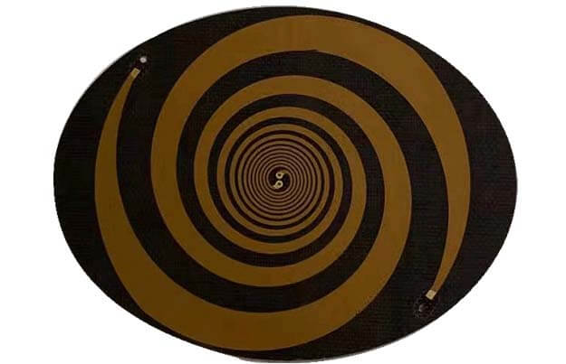
Double Sided PCB
What are the Properties of Double-Sided PCB?
The primary properties of the double-sided PCB are listed as under:
- They can conduct current from both sides of the PCB
- The conductive paths are present on the adjacent sides of the printed board circuit
- They allow closer routing traces for the current in the circuits
- They can alternate between the upper and inner layers
- They contain vias for better working
- They are less complex as compared to other PCB
- They include solder mask between the two layers of the PCB
- They conduct current with the help of different conductive pathways
- They have two-sided traces or paths for current to pass through the circuit

Properties of Double-Sided PCB
What are the Uses of Double-Sided PCB?
The uses or applications of the double-sided PCB are described as under:
- They are used in the converters of different appliances
- They are used in the regulators to control the amount of current flowing through the circuit
- Power conversion elements also include the double-sided PCB
- Instrumentation also makes the use of the double-sided PCB
- The majority of the control relays control the highest quality of two-layered PCB
- Power supplies are also the best applications of this PCB
- UPS systems and their batteries contain the premium quality of two-layered PCB
- The voltage regulators have the best two-layered PCB
- The motherboard of the Personal Computer is also made up of premium-level PCB
- This board is also used in the line reactors circuitry
- You’ll also find the double-sided PCB in the traffic control systems
- Many lightning devices are also known to operate with this type of PCB

Uses of Double-Sided PCB
What are the Advantages of Double-Sided PCB?
The advantages of the double-sided PCB are explained as under:
- Insulation
The two-layered PCBs are mainly made up of insulation materials over the copper layers. That is why they are used for insulating circuits.
- General Manufacturing
The Chinese manufacturers, including the SMTFAB, consider manufacturing the double-sided PCB as a general manufacturing process.
- Sensible Choice
Many PCB experts have suggested purchasing the double-sided PCB since it can easily be used in different electrical projects.
- Low Production Price
Unlike all the other types of PCB, this one comes with a substantially low production cost. It includes the engraving and soldering of the parts at reasonable rates.
- Modern Applications
The use of the double-sided PCB is now used in all modern applications. Thus, they give technology a new turn.
You can contact SMTFAB to get your hands on the best double-sided printed board circuit.

Advantages of Double-Sided PCB
What are the Disadvantages of Double Sided PCB?
Some of the common disadvantages of the double-sided PCB are listed as under:
- They are not suitable for carrying heavy current around the circuit
- The copper wires in these PCBs can’t be easily healed
- They are available with the chances of overheat during the soldering process
- They are a bit complex than the single-layered PCB
- Manufacturers find it hard to manufacture the double-sided PCB

Disadvantages of Double Sided PCB
What is the Difference Between Double-Sided and Single PCB?
Some of the potential differences between the double-sided and single-sided PCB are listed as under:
- The double-sided PCB has only one current pathway, whereas the single-sided PCB has multiple ways for current conduction.
- They have copper traces on both the external layers of the PCB, but single-sided PCB has copper traces only on one side.
- They contain two layers of copper, whereas the single-layered PCB has only a single layer of copper.
- They act as an electric catalyst as compared to the single-layered PCB
- They come with an efficient conducting path when compared to the current pathways of the single-sided PCB
- Moreover, the double-sided PCB increases the core area, but single-layered PCB doesn’t increase the core area of conduction.
- There are many through-holes in the double-layered PCB, but there are no holes in the single-layered PCB
- They contain vias on both sides, but the single-layered PCBs include vias only on one side.
You can reach out SMTFAB for having a profound insight into the difference between single and double-layered PCB.

Difference Between Double Sided and Single PCB
What is the Designing of Double-Sided PCB?
The designing of the double-sided PCB and its electric components is done with the help of unique printing technology.
The basic design of the circuit board is made with a particular layout combined with wirings on both sides.
Make sure to connect both sides of the double-layered PCB while designing it. However, the manufacturers use PROTEL for drawing the highest quality of the PCB design.
Moreover, the double-layered PCB design is then made into a grid-shaped frame. The experts draw parallel lines on the printed circuit to show the electric current pathways.
After confirming the current pathways, the two different layers of the double-sided PCB are then joined with the help of vias.
The design of the double-sided PCB also contains an IC chip for making the signal loop area smaller, thereby reducing the radiation of the current in the circuit.

Designing of Double-Sided PCB
What is the Manufacturing Process of Double-Sided PCB?
The manufacturing process of the double-sided PCB comprises the following steps:
- Production of the Substrate and Base
The first step in manufacturing the double-sided PCB is producing a high-quality substrate and a stable base.
The base and substrate of the two-layered PCB are made up of premium quality fiberglass and epoxy resin.
- Lamination
After producing the double-sided substrate in the PCBs, the next step is the production of the copper foil.
The thin copper foil is then laminated on both sides of the substrate for better conduction of electricity.
- Addition of the Silk Screen and Solder Mask
Once you’re done with the lamination of the copper on the double-sided PCB, it’s time for the application of the solder mask.
After the application of the solder mask, a high-quality silkscreen is then added on the upper side of the solder mask. This screen is mainly used for adding the symbols and characters to the PCB.
- Removal of Extra Copper
The addition of the solder mask and silkscreen is then followed by the removal of the extra copper from both sides of the PCB.
The removal of the excess copper from the double sides of the PCB improves its current conduction capacity to a greater level.
- Inspection
After manufacturing the double-sided PCB, the manufacturers carry out an ultimate inspection of the PCB to ensure quality.

Manufacturing Process of Double-Sided PCB
How Does Double-Sided PCB Works?
The double-sided PCB works with the conductive surface on both its sides with the copper traces.
The copper traces along with the conducting pathways makes sure about the passage of current through the circuit.
In addition to this, there is a dielectric layer between the two circuit layers of the copper in the double-sided PCB.
This dielectric substance, along with the solder mask on both sides, plays the leading role in conducting the current through the copper traces present on the layers of the PCB.
However, the internal flow of the current and power is governed by the connection between the layers of the printed board circuit.
This connection between the two adjacent layers of the two-layered PCB is offered with the help of through-holes and electric components.
What is the Assembly of Double-Sided PCB?
The assembly of the double-sided PCB consists of many challenging steps. However, some of these steps are explained as under:
- Application of the Solder Paste
The first step in the assembly of the two-layered PCB is the application of high-quality solder paste. This paste is mainly applied to the soldered sections of the printed board circuit.
In addition to this, the solder paste is also applied to the component pads of the PCB. The parts of the solder paste as the tiny grains of a solder material and a flux.
Moreover, the manufacturers directly apply the solder paste to the board for attaching the components in the right place.
- Picking up the Components Together
After applying the solder paste on the board, the printed board circuit is passed through the machine. This machine can load the components on the circuit board.
Moreover, the tension of the solder paste makes sure to hold the components of the circuit board. This activity is mainly preferred for the waveform circuits of the double-sided PCBs.
You can also use glues to keep the components in the right place on the circuit board of the PCB.
- Soldering of the Board
Once all the parts are placed on the board and glues are applied, the board is sent to the soldering procedure. A soldering machine is used in this process.
The soldering machine is also used in the mounting assembly, and the PCB soldering method is used to assemble the double-sided PCB.
- Inspection
The last step in the assembly of the double-sided PCB is the final inspection to check whether every step is carried out correctly or not.
The majority of the manufacturers carry out manual inspections, whereas some manufacturers carry out the automatic assessment of the PCB.
SMTFAB is one Chinese manufacturer that produces the highest quality of assembled double-sided PCB at reasonable rates.

Assembly of Double-Sided PCB
What are the Steps to Solder Two-Sided PCB?
The steps for soldering the two-sided PCB are explained as under:
- Prepare the iron that is used for welding the double sides of the printed board circuit.
- Prepare the particular surface on which you want to solder the different parts of the double-layered PCB
- Make sure to start with a clean surface so that there will be no inconvenience ahead.
- Place all those circuit components which you want to solder on the board.
- Apply some substantial heat with the help of the heated iron
- After applying heat, try to add the solder to the joint to place the components on the printed board circuit.
- The last step is testing the correct alignment of the components on the board by the solder joint.

Steps to Solder Two-Sided PCB
Are Vias Present in Double-Sided PCB?
Yes, These vias are also present in the double-layered PCB, which help to join the two separate layers of the printed board circuit.
The two-layer printed board circuit contains copper-coated two different sides, joined together with the help of bridges.
These special types of bridges or connections between the two-sided PCB are known as vias.
In addition to this, small holes on the printed board circuit are also known as via. It is basically used to place the components on the board of the PCB.
These holes or vias are then covered by high-quality metal for connecting the circuits on the board sides.

Vias Present in Double-Sided PCB
What is the Best Place to Purchase the Double-Sided PCB?
There are many types of best manufacturers worldwide who make the highest quality of double-sided PCB, but China lies at the top of the list of marketplaces when it comes to purchasing the two-layered PCB.
The excellence of China’s PCB industry in manufacturing the two-layered PCB and its components also reliefs the customers to get the reliable quality of PCBs.
Many manufacturers in China are known to fulfill the need of their customers no matter either it is about the production or the customization of the double-sided PCB.
SMTFAB is also regarded as the best manufacturer for purchasing the two-layered PCB at very reasonable rates.
Besides the availability of PCB at reasonable rates, some other factors that are responsible for making China the best place for two-layered PCB production are:
- Use of all modern technologies in the production of high-quality PCB
- Inspection by the experienced individuals
- Fulfillment of all quality and safety standards while making the PCB
What is the Warranty of Double-Sided PCB?
The warranty period of the double-sided PCB ranges from three to five straight years.
However, you’ll find versatile warranty durations from different PCB manufacturers in China. Some of them also provide a lifetime warranty of the double-sided PCB.
Other than this, the warranty period of the PCB is associated with a bulk of services such as the installation, repair, and replacement of the defective models of the PCB.
Not all Chinese manufacturers provide these additional services with the warranty of the two-layered printed board circuit.
But if you want the manufacturer to conduct the installation or repair your defective PCB, you’ll have to pay the VISA fees of the worker coming your way.
How to Purchase the Best Double-Sided PCB?
You can choose the best double-sided PCB by following the given tips:
- Reduced Size of the Circuit Board
When you’re out purchasing the highest quality of the double-sided PCB, the first factor you need to consider is the reduced size of the printed board circuit.
The double-sided printed board circuit should be of a compact size so that you can adjust it in sensitive devices.
- Circuit Density
Another factor in determining double-sided printed board circuits is to check the circuit density. The circuit density of the printed board circuit is governed by the number of components present on the circuit.
Thus, make sure to check the high circuit density of the PCB whenever thinking to purchase it for your appliances.
- Low Cost
Almost all types of double-sided PCBs are available at reasonable costs at many manufacturers. Thus, make sure about your affordability range whenever purchasing high-quality PCBs.
The low cost of the printed board circuits doesn’t mean the low quality of the circuit board.
You can contact efficient Chinese manufacturers like SMTFAB to get the highest quality of PCB.

Purchase the Best Double-Sided PCB
How Many Layers Are Present in the Double-Sided PCB?
There are two main layers in the double-sided PCBs, which play an essential role in the conduction of electricity through the circuit of electrical appliances.
In addition to this, both compact layers on either side of the PCB are made up of premium quality copper. Thus you don’t have to bother about the current conduction.
Both two layers of the PCB contain the traces or paths on the copper layers which govern the conduction of electricity.
Besides this, the two layers are joined together with the help of highly compact vias of through-holes.
These holes are also responsible for the conduction of current through different circuits or layers within the board.
How to Import Double-Sided PCB In Bulk From China?
You can import the double-sided PCB in bulk from China by following the given steps:
- Contact the most efficient manufacturer in China
- Contact their support team for getting an idea of the items present
- Choose your best pick about the double-layered circuits
- Check the availability of all those documents that are required for the import of the PCB
- Ask the manufacturer to import the PCB to your address
How to Choose the Best Manufacturer of Double-Sided PCB?
You can choose the best manufacturer of double-sided PCB by following the given steps:
- Choose the Right Manufacturer
The bulk amount of the manufacturers in China may confuse you. But you have to choose the right type of manufacturer by exploring the options on the online sites.
- Contact the Manufacturer
After selecting the proper manufacturer, the next step is to reach them through their email or phone number. Try to contact the support team of the manufacturers for better assistance.
- Select Your Item
Once you’ve selected the manufacturer and contacted them, the next step is to choose the right type of double-sided printed board circuit for your device.
- Check the R&D Services
Make sure that the manufacturer you’re going to choose has the R&D services. It is essential to check the R&D services for the availability of modern technologies in the production of PCB.
- Quality of Manufacturing Process
There’s no need for you to compromise on the manufacturing quality of the PCB. For checking the right manufacturing platform of the PCB, make sure to visit the site of the supplier.
- One-Stop Solution
The manufacturer that you’re thinking to purchase should have to provide a one-stop solution for solving the problems of its customers.
- Quality Certifications
Check the availability of the quality certifications at the manufacturer’s site for the assurance of high-quality products.
- Experience of Manufacturing
The manufacturer should hold more than ten years of construction experience in the production of double-sided printed board circuits.
SMTFAB can be your best pick if you want to get your hands on the most reliable PCB manufacturers in China.
Your Reliable Double-Sided PCB Manufacturer in China
SMTFAB is a China top double-sided PCB manufacturer and supplier in China. When you have a double-sided PCB inquiry, send it now.
- Over 12 years double-sided PCB manufacturing experience
- Files receive full CAM review prior to manufacturing
- Certified with UL US and Canada
- 24h Quick-turn service for your prototype PCB
- 100% E-test and AOI inspection
- Provide WIP(work in process) report to you each week
- 7/24 sales and engineering tech support
- Production Facility
- Capabilities
| Item | Capability |
| Layer Count | 1-40layers |
| Base Material | KB、Shengyi、ShengyiSF305、FR408、FR408HR、IS410、FR406、GETEK、370HR、IT180A、Rogers4350、Rogers4000、PTFE Laminates(Rogers series、Taconic series、Arlon series、Nelco series)、Rogers/Taconic/Arlon/Nelco laminate with FR-4 material(including partial Ro4350B hybrid laminating with FR-4) |
| Board Type | Backplane、HDI、High multi-layer blind&buried PCB、Embedded Capacitance、Embedded resistance board 、Heavy copper power PCB、Backdrill, PCB Gold Finger |
| Board Thickness | 0.2-5.0mm |
| Copper Thickness | Min. 1/2 OZ, Max. 10 OZ |
| PTH Wall | 25um(1mil) |
| Maximum Board Size | 1100*500mm(43”*19”) |
| Min laser drilling size | 4mil |
| Min. Spacing/Tracing | 2.7mil/2.7mil |
| Solder Mask | Green, Black, Blue, Red, White, Yellow, Purple matte/glossy |
| Surface Treatment | Flash gold(electroplated gold)、ENIG、Hard gold、Flash gold、HASL Lead-free 、OSP、ENEPIG、Soft gold、Immersion silver、Immersion Tin、ENIG+OSP, ENIG+Gold finger, Flash gold(electroplated gold)+Gold finger(50u”), Immersion silver+Gold finger, Immersion Tin+Gold finger |
| Min. Annular Ring | 3mil |
| Aspect ratio | 10:1(HASL Lead-free 、HASL Lead、ENIG、Immersion Tin、Immersion silver、ENEPIG);8:1(OSP) |
| Impedance control | ±5ohm(<50ohm), ±10%(≥50ohm) |
| Other Techniques | Blind/Buried Via |
| Gold Fingers | |
| Press Fit | |
| Via in Pad | |
| Electrical Test |
Releted Other PCBs
Why Choose SMTFAB for Your Double-Sided PCB
Double-Sided PCBs (also known as Double-Sided Plated Thru) is very normal in the PCB industry and you can find them in many electronic products.
As a valuable double-sided PCB manufacturer and factory in China, SMTFAB can offer you many different kinds of double-sided PCBs, including LED PCB, metal core circuit board, aluminum PCB, flexible circuit board, high-frequency PCB, Rogers printed circuit board, ceramic PCB, and Teflon PCB.
Single-sided PCBs have a conductive surface, while double-sided PCBs have a conductive layer on each side.
Our double-sided PCB has full of top quality and is long-lasting to use. It can widely use in LED lighting, power convention, power supplier, phone systems, traffic systems, printers, and hard drives.
If you are looking for a trusted and reliable double-sided PCB supplier? SMTFAB is your perfect choice.
We can help you to offer your double-sided PCB with a 100% reliable product. SMTFAB has strictly controlled the incoming material for each process and ensure to provide high quality to our customers.
SMTFAB has more than 500 employees with over 12 years of PCB manufacturing experience and the workshop area will be reached 20,000 square meters.
We can offer free samples for you when you have mass production order of double-sided circuit boards.
We specialize in offering original double-sided PCB design, fabrication, and assembly. We can provide a one-stop solution for your project.
When you have any urgent double-sided printed circuit board, please send it to us. SMTFAB can help you to produce it with 24h.
Please do not hesitate to contact us, we’re always here to support you.
Double-Sided PCB: The Ultimate FAQ Guide
Do you need to upgrade your gadgets with highly advanced technology systems?
Or are you thinking of allowing a more efficient current flow in your technical applications?
If so, don’t worry! We’ve got your back!
Double-sided PCB can be the ultimate solution to both of these queries.
The guide below has collected the commonly asked questions about this common type of printed board circuit.
So let’s explore what’s ahead!
- What is Double Sided PCB?
- What are the Properties of Double-Sided PCB?
- What are the Uses of Double-Sided PCB?
- What are the Advantages of Double-Sided PCB?
- What are the Disadvantages of Double Sided PCB?
- What is the Difference Between Double-Sided and Single PCB?
- What is the Designing of Double-Sided PCB?
- What is the Manufacturing Process of Double-Sided PCB?
- How Does Double-Sided PCB Works?
- What is the Assembly of Double-Sided PCB?
- What are the Steps to Solder Two-Sided PCB?
- Are Vias Present in Double-Sided PCB?
- What is the Best Place to Purchase the Double-Sided PCB
- What is the Warranty of Double-Sided PCB?
- How to Purchase the Best Double-Sided PCB?
- How Many Layers Are Present in the Double-Sided PCB?
- How to Import Double-Sided PCB In Bulk From China?
- How to Choose the Best Manufacturer of Double-Sided PCB?
What is Double Sided PCB?
Double-sided PCB is defined as the particular type of printed board circuit containing the circuit traces on both sides.
The two different faces of this particular type of PCB are connected through the plated holes.
They are considered as a complex type of PCBs as compared to single-sided PCBs. The conductivity of current through this PCB is governed with the help of plated holes and electronic components.
In addition to this, these PCB holes allow the different sides of the PCB to connect.
The two layers of the PCB are also known as the two conducting paths of current in the electric circuits.
Double-sided PCB is famous for many electronic appliances which we use every day. The conductive layers on both sides of PCB are covered with copper laminations.
The copper layers are then integrated with the solder mask installed between the two different layers of the PCB.
Moreover, this type of PCB is known for not offering an extensive range of complexity compared to the three-layer or multi-layer printed board circuits.
Double Sided PCB
What are the Properties of Double-Sided PCB?
The primary properties of the double-sided PCB are listed as under:
- They can conduct current from both sides of the PCB
- The conductive paths are present on the adjacent sides of the printed board circuit
- They allow closer routing traces for the current in the circuits
- They can alternate between the upper and inner layers
- They contain vias for better working
- They are less complex as compared to other PCB
- They include solder mask between the two layers of the PCB
- They conduct current with the help of different conductive pathways
- They have two-sided traces or paths for current to pass through the circuit
Properties of Double-Sided PCB
What are the Uses of Double-Sided PCB?
The uses or applications of the double-sided PCB are described as under:
- They are used in the converters of different appliances
- They are used in the regulators to control the amount of current flowing through the circuit
- Power conversion elements also include the double-sided PCB
- Instrumentation also makes the use of the double-sided PCB
- The majority of the control relays control the highest quality of two-layered PCB
- Power supplies are also the best applications of this PCB
- UPS systems and their batteries contain the premium quality of two-layered PCB
- The voltage regulators have the best two-layered PCB
- The motherboard of the Personal Computer is also made up of premium-level PCB
- This board is also used in the line reactors circuitry
- You’ll also find the double-sided PCB in the traffic control systems
- Many lightning devices are also known to operate with this type of PCB
Uses of Double-Sided PCB
What are the Advantages of Double-Sided PCB?
The advantages of the double-sided PCB are explained as under:
- Insulation
The two-layered PCBs are mainly made up of insulation materials over the copper layers. That is why they are used for insulating circuits.
- General Manufacturing
The Chinese manufacturers, including the SMTFAB, consider manufacturing the double-sided PCB as a general manufacturing process.
- Sensible Choice
Many PCB experts have suggested purchasing the double-sided PCB since it can easily be used in different electrical projects.
- Low Production Price
Unlike all the other types of PCB, this one comes with a substantially low production cost. It includes the engraving and soldering of the parts at reasonable rates.
- Modern Applications
The use of the double-sided PCB is now used in all modern applications. Thus, they give technology a new turn.
You can contact SMTFAB to get your hands on the best double-sided printed board circuit.
Advantages of Double-Sided PCB
What are the Disadvantages of Double Sided PCB?
Some of the common disadvantages of the double-sided PCB are listed as under:
- They are not suitable for carrying heavy current around the circuit
- The copper wires in these PCBs can’t be easily healed
- They are available with the chances of overheat during the soldering process
- They are a bit complex than the single-layered PCB
- Manufacturers find it hard to manufacture the double-sided PCB
Disadvantages of Double Sided PCB
What is the Difference Between Double-Sided and Single PCB?
Some of the potential differences between the double-sided and single-sided PCB are listed as under:
- The double-sided PCB has only one current pathway, whereas the single-sided PCB has multiple ways for current conduction.
- They have copper traces on both the external layers of the PCB, but single-sided PCB has copper traces only on one side.
- They contain two layers of copper, whereas the single-layered PCB has only a single layer of copper.
- They act as an electric catalyst as compared to the single-layered PCB
- They come with an efficient conducting path when compared to the current pathways of the single-sided PCB
- Moreover, the double-sided PCB increases the core area, but single-layered PCB doesn’t increase the core area of conduction.
- There are many through-holes in the double-layered PCB, but there are no holes in the single-layered PCB
- They contain vias on both sides, but the single-layered PCBs include vias only on one side.
You can reach out SMTFAB for having a profound insight into the difference between single and double-layered PCB.
Difference Between Double Sided and Single PCB
What is the Designing of Double-Sided PCB?
The designing of the double-sided PCB and its electric components is done with the help of unique printing technology.
The basic design of the circuit board is made with a particular layout combined with wirings on both sides.
Make sure to connect both sides of the double-layered PCB while designing it. However, the manufacturers use PROTEL for drawing the highest quality of the PCB design.
Moreover, the double-layered PCB design is then made into a grid-shaped frame. The experts draw parallel lines on the printed circuit to show the electric current pathways.
After confirming the current pathways, the two different layers of the double-sided PCB are then joined with the help of vias.
The design of the double-sided PCB also contains an IC chip for making the signal loop area smaller, thereby reducing the radiation of the current in the circuit.
Designing of Double-Sided PCB
What is the Manufacturing Process of Double-Sided PCB?
The manufacturing process of the double-sided PCB comprises the following steps:
- Production of the Substrate and Base
The first step in manufacturing the double-sided PCB is producing a high-quality substrate and a stable base.
The base and substrate of the two-layered PCB are made up of premium quality fiberglass and epoxy resin.
- Lamination
After producing the double-sided substrate in the PCBs, the next step is the production of the copper foil.
The thin copper foil is then laminated on both sides of the substrate for better conduction of electricity.
- Addition of the Silk Screen and Solder Mask
Once you’re done with the lamination of the copper on the double-sided PCB, it’s time for the application of the solder mask.
After the application of the solder mask, a high-quality silkscreen is then added on the upper side of the solder mask. This screen is mainly used for adding the symbols and characters to the PCB.
- Removal of Extra Copper
The addition of the solder mask and silkscreen is then followed by the removal of the extra copper from both sides of the PCB.
The removal of the excess copper from the double sides of the PCB improves its current conduction capacity to a greater level.
- Inspection
After manufacturing the double-sided PCB, the manufacturers carry out an ultimate inspection of the PCB to ensure quality.
Manufacturing Process of Double-Sided PCB
How Does Double-Sided PCB Works?
The double-sided PCB works with the conductive surface on both its sides with the copper traces.
The copper traces along with the conducting pathways makes sure about the passage of current through the circuit.
In addition to this, there is a dielectric layer between the two circuit layers of the copper in the double-sided PCB.
This dielectric substance, along with the solder mask on both sides, plays the leading role in conducting the current through the copper traces present on the layers of the PCB.
However, the internal flow of the current and power is governed by the connection between the layers of the printed board circuit.
This connection between the two adjacent layers of the two-layered PCB is offered with the help of through-holes and electric components.
What is the Assembly of Double-Sided PCB?
The assembly of the double-sided PCB consists of many challenging steps. However, some of these steps are explained as under:
- Application of the Solder Paste
The first step in the assembly of the two-layered PCB is the application of high-quality solder paste. This paste is mainly applied to the soldered sections of the printed board circuit.
In addition to this, the solder paste is also applied to the component pads of the PCB. The parts of the solder paste as the tiny grains of a solder material and a flux.
Moreover, the manufacturers directly apply the solder paste to the board for attaching the components in the right place.
- Picking up the Components Together
After applying the solder paste on the board, the printed board circuit is passed through the machine. This machine can load the components on the circuit board.
Moreover, the tension of the solder paste makes sure to hold the components of the circuit board. This activity is mainly preferred for the waveform circuits of the double-sided PCBs.
You can also use glues to keep the components in the right place on the circuit board of the PCB.
- Soldering of the Board
Once all the parts are placed on the board and glues are applied, the board is sent to the soldering procedure. A soldering machine is used in this process.
The soldering machine is also used in the mounting assembly, and the PCB soldering method is used to assemble the double-sided PCB.
- Inspection
The last step in the assembly of the double-sided PCB is the final inspection to check whether every step is carried out correctly or not.
The majority of the manufacturers carry out manual inspections, whereas some manufacturers carry out the automatic assessment of the PCB.
SMTFAB is one Chinese manufacturer that produces the highest quality of assembled double-sided PCB at reasonable rates.
Assembly of Double-Sided PCB
What are the Steps to Solder Two-Sided PCB?
The steps for soldering the two-sided PCB are explained as under:
- Prepare the iron that is used for welding the double sides of the printed board circuit.
- Prepare the particular surface on which you want to solder the different parts of the double-layered PCB
- Make sure to start with a clean surface so that there will be no inconvenience ahead.
- Place all those circuit components which you want to solder on the board.
- Apply some substantial heat with the help of the heated iron
- After applying heat, try to add the solder to the joint to place the components on the printed board circuit.
- The last step is testing the correct alignment of the components on the board by the solder joint.
Steps to Solder Two-Sided PCB
Are Vias Present in Double-Sided PCB?
Yes, These vias are also present in the double-layered PCB, which help to join the two separate layers of the printed board circuit.
The two-layer printed board circuit contains copper-coated two different sides, joined together with the help of bridges.
These special types of bridges or connections between the two-sided PCB are known as vias.
In addition to this, small holes on the printed board circuit are also known as via. It is basically used to place the components on the board of the PCB.
These holes or vias are then covered by high-quality metal for connecting the circuits on the board sides.
Vias Present in Double-Sided PCB
What is the Best Place to Purchase the Double-Sided PCB?
There are many types of best manufacturers worldwide who make the highest quality of double-sided PCB, but China lies at the top of the list of marketplaces when it comes to purchasing the two-layered PCB.
The excellence of China’s PCB industry in manufacturing the two-layered PCB and its components also reliefs the customers to get the reliable quality of PCBs.
Many manufacturers in China are known to fulfill the need of their customers no matter either it is about the production or the customization of the double-sided PCB.
SMTFAB is also regarded as the best manufacturer for purchasing the two-layered PCB at very reasonable rates.
Besides the availability of PCB at reasonable rates, some other factors that are responsible for making China the best place for two-layered PCB production are:
- Use of all modern technologies in the production of high-quality PCB
- Inspection by the experienced individuals
- Fulfillment of all quality and safety standards while making the PCB
What is the Warranty of Double-Sided PCB?
The warranty period of the double-sided PCB ranges from three to five straight years.
However, you’ll find versatile warranty durations from different PCB manufacturers in China. Some of them also provide a lifetime warranty of the double-sided PCB.
Other than this, the warranty period of the PCB is associated with a bulk of services such as the installation, repair, and replacement of the defective models of the PCB.
Not all Chinese manufacturers provide these additional services with the warranty of the two-layered printed board circuit.
But if you want the manufacturer to conduct the installation or repair your defective PCB, you’ll have to pay the VISA fees of the worker coming your way.
How to Purchase the Best Double-Sided PCB?
You can choose the best double-sided PCB by following the given tips:
- Reduced Size of the Circuit Board
When you’re out purchasing the highest quality of the double-sided PCB, the first factor you need to consider is the reduced size of the printed board circuit.
The double-sided printed board circuit should be of a compact size so that you can adjust it in sensitive devices.
- Circuit Density
Another factor in determining double-sided printed board circuits is to check the circuit density. The circuit density of the printed board circuit is governed by the number of components present on the circuit.
Thus, make sure to check the high circuit density of the PCB whenever thinking to purchase it for your appliances.
- Low Cost
Almost all types of double-sided PCBs are available at reasonable costs at many manufacturers. Thus, make sure about your affordability range whenever purchasing high-quality PCBs.
The low cost of the printed board circuits doesn’t mean the low quality of the circuit board.
You can contact efficient Chinese manufacturers like SMTFAB to get the highest quality of PCB.
Purchase the Best Double-Sided PCB
How Many Layers Are Present in the Double-Sided PCB?
There are two main layers in the double-sided PCBs, which play an essential role in the conduction of electricity through the circuit of electrical appliances.
In addition to this, both compact layers on either side of the PCB are made up of premium quality copper. Thus you don’t have to bother about the current conduction.
Both two layers of the PCB contain the traces or paths on the copper layers which govern the conduction of electricity.
Besides this, the two layers are joined together with the help of highly compact vias of through-holes.
These holes are also responsible for the conduction of current through different circuits or layers within the board.
How to Import Double-Sided PCB In Bulk From China?
You can import the double-sided PCB in bulk from China by following the given steps:
- Contact the most efficient manufacturer in China
- Contact their support team for getting an idea of the items present
- Choose your best pick about the double-layered circuits
- Check the availability of all those documents that are required for the import of the PCB
- Ask the manufacturer to import the PCB to your address
How to Choose the Best Manufacturer of Double-Sided PCB?
You can choose the best manufacturer of double-sided PCB by following the given steps:
- Choose the Right Manufacturer
The bulk amount of the manufacturers in China may confuse you. But you have to choose the right type of manufacturer by exploring the options on the online sites.
- Contact the Manufacturer
After selecting the proper manufacturer, the next step is to reach them through their email or phone number. Try to contact the support team of the manufacturers for better assistance.
- Select Your Item
Once you’ve selected the manufacturer and contacted them, the next step is to choose the right type of double-sided printed board circuit for your device.
- Check the R&D Services
Make sure that the manufacturer you’re going to choose has the R&D services. It is essential to check the R&D services for the availability of modern technologies in the production of PCB.
- Quality of Manufacturing Process
There’s no need for you to compromise on the manufacturing quality of the PCB. For checking the right manufacturing platform of the PCB, make sure to visit the site of the supplier.
- One-Stop Solution
The manufacturer that you’re thinking to purchase should have to provide a one-stop solution for solving the problems of its customers.
- Quality Certifications
Check the availability of the quality certifications at the manufacturer’s site for the assurance of high-quality products.
- Experience of Manufacturing
The manufacturer should hold more than ten years of construction experience in the production of double-sided printed board circuits.
SMTFAB can be your best pick if you want to get your hands on the most reliable PCB manufacturers in China.
Your Reliable Double-Sided PCB Manufacturer in China
SMTFAB is a China top double-sided PCB manufacturer and supplier in China. When you have a double-sided PCB inquiry, send it now.
- Over 12 years double-sided PCB manufacturing experience
- Files receive full CAM review prior to manufacturing
- Certified with UL US and Canada
- 24h Quick-turn service for your prototype PCB
- 100% E-test and AOI inspection
- Provide WIP(work in process) report to you each week
- 7/24 sales and engineering tech support
Your Reliable Double-Sided PCB Manufacturer in China
Your Reliable Double-Sided PCB Manufacturer in China
SMTFAB is a China top double-sided PCB manufacturer and supplier in China. When you have a double-sided PCB inquiry, send it now.
- Over 12 years double-sided PCB manufacturing experience
- Files receive full CAM review prior to manufacturing
- Certified with UL US and Canada
- 24h Quick-turn service for your prototype PCB
- 100% E-test and AOI inspection
- Provide WIP(work in process) report to you each week
- 7/24 sales and engineering tech support
- Production Facility
- Capabilities
| Item | Capability |
| Layer Count | 1-40layers |
| Base Material | KB、Shengyi、ShengyiSF305、FR408、FR408HR、IS410、FR406、GETEK、370HR、IT180A、Rogers4350、Rogers4000、PTFE Laminates(Rogers series、Taconic series、Arlon series、Nelco series)、Rogers/Taconic/Arlon/Nelco laminate with FR-4 material(including partial Ro4350B hybrid laminating with FR-4) |
| Board Type | Backplane、HDI、High multi-layer blind&buried PCB、Embedded Capacitance、Embedded resistance board 、Heavy copper power PCB、Backdrill, PCB Gold Finger |
| Board Thickness | 0.2-5.0mm |
| Copper Thickness | Min. 1/2 OZ, Max. 10 OZ |
| PTH Wall | 25um(1mil) |
| Maximum Board Size | 1100*500mm(43”*19”) |
| Min laser drilling size | 4mil |
| Min. Spacing/Tracing | 2.7mil/2.7mil |
| Solder Mask | Green, Black, Blue, Red, White, Yellow, Purple matte/glossy |
| Surface Treatment | Flash gold(electroplated gold)、ENIG、Hard gold、Flash gold、HASL Lead-free 、OSP、ENEPIG、Soft gold、Immersion silver、Immersion Tin、ENIG+OSP, ENIG+Gold finger, Flash gold(electroplated gold)+Gold finger(50u”), Immersion silver+Gold finger, Immersion Tin+Gold finger |
| Min. Annular Ring | 3mil |
| Aspect ratio | 10:1(HASL Lead-free 、HASL Lead、ENIG、Immersion Tin、Immersion silver、ENEPIG);8:1(OSP) |
| Impedance control | ±5ohm(<50ohm), ±10%(≥50ohm) |
| Other Techniques | Blind/Buried Via |
| Gold Fingers | |
| Press Fit | |
| Via in Pad | |
| Electrical Test |
Why Choose SMTFAB for Your Double-Sided PCB
Double-Sided PCBs (also known as Double-Sided Plated Thru) is very normal in the PCB industry and you can find them in many electronic products.
As a valuable double-sided PCB manufacturer and factory in China, SMTFAB can offer you many different kinds of double-sided PCBs, including LED PCB, metal core circuit board, aluminum PCB, flexible circuit board, high-frequency PCB, Rogers printed circuit board, ceramic PCB, and Teflon PCB.
Single-sided PCBs have a conductive surface, while double-sided PCBs have a conductive layer on each side.
Our double-sided PCB has full of top quality and is long-lasting to use. It can widely use in LED lighting, power convention, power supplier, phone systems, traffic systems, printers, and hard drives.
If you are looking for a trusted and reliable double-sided PCB supplier? SMTFAB is your perfect choice.
We can help you to offer your double-sided PCB with a 100% reliable product. SMTFAB has strictly controlled the incoming material for each process and ensure to provide high quality to our customers.
SMTFAB has more than 500 employees with over 12 years of PCB manufacturing experience and the workshop area will be reached 20,000 square meters.
We can offer free samples for you when you have mass production order of double-sided circuit boards.
We specialize in offering original double-sided PCB design, fabrication, and assembly. We can provide a one-stop solution for your project.
When you have any urgent double-sided printed circuit board, please send it to us. SMTFAB can help you to produce it with 24h.
Please do not hesitate to contact us, we’re always here to support you.
Double-Sided PCB: The Ultimate FAQ Guide
Do you need to upgrade your gadgets with highly advanced technology systems?
Or are you thinking of allowing a more efficient current flow in your technical applications?
If so, don’t worry! We’ve got your back!
Double-sided PCB can be the ultimate solution to both of these queries.
The guide below has collected the commonly asked questions about this common type of printed board circuit.
So let’s explore what’s ahead!
- What is Double Sided PCB?
- What are the Properties of Double-Sided PCB?
- What are the Uses of Double-Sided PCB?
- What are the Advantages of Double-Sided PCB?
- What are the Disadvantages of Double Sided PCB?
- What is the Difference Between Double-Sided and Single PCB?
- What is the Designing of Double-Sided PCB?
- What is the Manufacturing Process of Double-Sided PCB?
- How Does Double-Sided PCB Works?
- What is the Assembly of Double-Sided PCB?
- What are the Steps to Solder Two-Sided PCB?
- Are Vias Present in Double-Sided PCB?
- What is the Best Place to Purchase the Double-Sided PCB
- What is the Warranty of Double-Sided PCB?
- How to Purchase the Best Double-Sided PCB?
- How Many Layers Are Present in the Double-Sided PCB?
- How to Import Double-Sided PCB In Bulk From China?
- How to Choose the Best Manufacturer of Double-Sided PCB?
What is Double Sided PCB?
Double-sided PCB is defined as the particular type of printed board circuit containing the circuit traces on both sides.
The two different faces of this particular type of PCB are connected through the plated holes.
They are considered as a complex type of PCBs as compared to single-sided PCBs. The conductivity of current through this PCB is governed with the help of plated holes and electronic components.
In addition to this, these PCB holes allow the different sides of the PCB to connect.
The two layers of the PCB are also known as the two conducting paths of current in the electric circuits.
Double-sided PCB is famous for many electronic appliances which we use every day. The conductive layers on both sides of PCB are covered with copper laminations.
The copper layers are then integrated with the solder mask installed between the two different layers of the PCB.
Moreover, this type of PCB is known for not offering an extensive range of complexity compared to the three-layer or multi-layer printed board circuits.
Double Sided PCB
What are the Properties of Double-Sided PCB?
The primary properties of the double-sided PCB are listed as under:
- They can conduct current from both sides of the PCB
- The conductive paths are present on the adjacent sides of the printed board circuit
- They allow closer routing traces for the current in the circuits
- They can alternate between the upper and inner layers
- They contain vias for better working
- They are less complex as compared to other PCB
- They include solder mask between the two layers of the PCB
- They conduct current with the help of different conductive pathways
- They have two-sided traces or paths for current to pass through the circuit
Properties of Double-Sided PCB
What are the Uses of Double-Sided PCB?
The uses or applications of the double-sided PCB are described as under:
- They are used in the converters of different appliances
- They are used in the regulators to control the amount of current flowing through the circuit
- Power conversion elements also include the double-sided PCB
- Instrumentation also makes the use of the double-sided PCB
- The majority of the control relays control the highest quality of two-layered PCB
- Power supplies are also the best applications of this PCB
- UPS systems and their batteries contain the premium quality of two-layered PCB
- The voltage regulators have the best two-layered PCB
- The motherboard of the Personal Computer is also made up of premium-level PCB
- This board is also used in the line reactors circuitry
- You’ll also find the double-sided PCB in the traffic control systems
- Many lightning devices are also known to operate with this type of PCB
Uses of Double-Sided PCB
What are the Advantages of Double-Sided PCB?
The advantages of the double-sided PCB are explained as under:
- Insulation
The two-layered PCBs are mainly made up of insulation materials over the copper layers. That is why they are used for insulating circuits.
- General Manufacturing
The Chinese manufacturers, including the SMTFAB, consider manufacturing the double-sided PCB as a general manufacturing process.
- Sensible Choice
Many PCB experts have suggested purchasing the double-sided PCB since it can easily be used in different electrical projects.
- Low Production Price
Unlike all the other types of PCB, this one comes with a substantially low production cost. It includes the engraving and soldering of the parts at reasonable rates.
- Modern Applications
The use of the double-sided PCB is now used in all modern applications. Thus, they give technology a new turn.
You can contact SMTFAB to get your hands on the best double-sided printed board circuit.
Advantages of Double-Sided PCB
What are the Disadvantages of Double Sided PCB?
Some of the common disadvantages of the double-sided PCB are listed as under:
- They are not suitable for carrying heavy current around the circuit
- The copper wires in these PCBs can’t be easily healed
- They are available with the chances of overheat during the soldering process
- They are a bit complex than the single-layered PCB
- Manufacturers find it hard to manufacture the double-sided PCB
Disadvantages of Double Sided PCB
What is the Difference Between Double-Sided and Single PCB?
Some of the potential differences between the double-sided and single-sided PCB are listed as under:
- The double-sided PCB has only one current pathway, whereas the single-sided PCB has multiple ways for current conduction.
- They have copper traces on both the external layers of the PCB, but single-sided PCB has copper traces only on one side.
- They contain two layers of copper, whereas the single-layered PCB has only a single layer of copper.
- They act as an electric catalyst as compared to the single-layered PCB
- They come with an efficient conducting path when compared to the current pathways of the single-sided PCB
- Moreover, the double-sided PCB increases the core area, but single-layered PCB doesn’t increase the core area of conduction.
- There are many through-holes in the double-layered PCB, but there are no holes in the single-layered PCB
- They contain vias on both sides, but the single-layered PCBs include vias only on one side.
You can reach out SMTFAB for having a profound insight into the difference between single and double-layered PCB.
Difference Between Double Sided and Single PCB
What is the Designing of Double-Sided PCB?
The designing of the double-sided PCB and its electric components is done with the help of unique printing technology.
The basic design of the circuit board is made with a particular layout combined with wirings on both sides.
Make sure to connect both sides of the double-layered PCB while designing it. However, the manufacturers use PROTEL for drawing the highest quality of the PCB design.
Moreover, the double-layered PCB design is then made into a grid-shaped frame. The experts draw parallel lines on the printed circuit to show the electric current pathways.
After confirming the current pathways, the two different layers of the double-sided PCB are then joined with the help of vias.
The design of the double-sided PCB also contains an IC chip for making the signal loop area smaller, thereby reducing the radiation of the current in the circuit.
Designing of Double-Sided PCB
What is the Manufacturing Process of Double-Sided PCB?
The manufacturing process of the double-sided PCB comprises the following steps:
- Production of the Substrate and Base
The first step in manufacturing the double-sided PCB is producing a high-quality substrate and a stable base.
The base and substrate of the two-layered PCB are made up of premium quality fiberglass and epoxy resin.
- Lamination
After producing the double-sided substrate in the PCBs, the next step is the production of the copper foil.
The thin copper foil is then laminated on both sides of the substrate for better conduction of electricity.
- Addition of the Silk Screen and Solder Mask
Once you’re done with the lamination of the copper on the double-sided PCB, it’s time for the application of the solder mask.
After the application of the solder mask, a high-quality silkscreen is then added on the upper side of the solder mask. This screen is mainly used for adding the symbols and characters to the PCB.
- Removal of Extra Copper
The addition of the solder mask and silkscreen is then followed by the removal of the extra copper from both sides of the PCB.
The removal of the excess copper from the double sides of the PCB improves its current conduction capacity to a greater level.
- Inspection
After manufacturing the double-sided PCB, the manufacturers carry out an ultimate inspection of the PCB to ensure quality.
Manufacturing Process of Double-Sided PCB
How Does Double-Sided PCB Works?
The double-sided PCB works with the conductive surface on both its sides with the copper traces.
The copper traces along with the conducting pathways makes sure about the passage of current through the circuit.
In addition to this, there is a dielectric layer between the two circuit layers of the copper in the double-sided PCB.
This dielectric substance, along with the solder mask on both sides, plays the leading role in conducting the current through the copper traces present on the layers of the PCB.
However, the internal flow of the current and power is governed by the connection between the layers of the printed board circuit.
This connection between the two adjacent layers of the two-layered PCB is offered with the help of through-holes and electric components.
What is the Assembly of Double-Sided PCB?
The assembly of the double-sided PCB consists of many challenging steps. However, some of these steps are explained as under:
- Application of the Solder Paste
The first step in the assembly of the two-layered PCB is the application of high-quality solder paste. This paste is mainly applied to the soldered sections of the printed board circuit.
In addition to this, the solder paste is also applied to the component pads of the PCB. The parts of the solder paste as the tiny grains of a solder material and a flux.
Moreover, the manufacturers directly apply the solder paste to the board for attaching the components in the right place.
- Picking up the Components Together
After applying the solder paste on the board, the printed board circuit is passed through the machine. This machine can load the components on the circuit board.
Moreover, the tension of the solder paste makes sure to hold the components of the circuit board. This activity is mainly preferred for the waveform circuits of the double-sided PCBs.
You can also use glues to keep the components in the right place on the circuit board of the PCB.
- Soldering of the Board
Once all the parts are placed on the board and glues are applied, the board is sent to the soldering procedure. A soldering machine is used in this process.
The soldering machine is also used in the mounting assembly, and the PCB soldering method is used to assemble the double-sided PCB.
- Inspection
The last step in the assembly of the double-sided PCB is the final inspection to check whether every step is carried out correctly or not.
The majority of the manufacturers carry out manual inspections, whereas some manufacturers carry out the automatic assessment of the PCB.
SMTFAB is one Chinese manufacturer that produces the highest quality of assembled double-sided PCB at reasonable rates.
Assembly of Double-Sided PCB
What are the Steps to Solder Two-Sided PCB?
The steps for soldering the two-sided PCB are explained as under:
- Prepare the iron that is used for welding the double sides of the printed board circuit.
- Prepare the particular surface on which you want to solder the different parts of the double-layered PCB
- Make sure to start with a clean surface so that there will be no inconvenience ahead.
- Place all those circuit components which you want to solder on the board.
- Apply some substantial heat with the help of the heated iron
- After applying heat, try to add the solder to the joint to place the components on the printed board circuit.
- The last step is testing the correct alignment of the components on the board by the solder joint.
Steps to Solder Two-Sided PCB
Are Vias Present in Double-Sided PCB?
Yes, These vias are also present in the double-layered PCB, which help to join the two separate layers of the printed board circuit.
The two-layer printed board circuit contains copper-coated two different sides, joined together with the help of bridges.
These special types of bridges or connections between the two-sided PCB are known as vias.
In addition to this, small holes on the printed board circuit are also known as via. It is basically used to place the components on the board of the PCB.
These holes or vias are then covered by high-quality metal for connecting the circuits on the board sides.
Vias Present in Double-Sided PCB
What is the Best Place to Purchase the Double-Sided PCB?
There are many types of best manufacturers worldwide who make the highest quality of double-sided PCB, but China lies at the top of the list of marketplaces when it comes to purchasing the two-layered PCB.
The excellence of China’s PCB industry in manufacturing the two-layered PCB and its components also reliefs the customers to get the reliable quality of PCBs.
Many manufacturers in China are known to fulfill the need of their customers no matter either it is about the production or the customization of the double-sided PCB.
SMTFAB is also regarded as the best manufacturer for purchasing the two-layered PCB at very reasonable rates.
Besides the availability of PCB at reasonable rates, some other factors that are responsible for making China the best place for two-layered PCB production are:
- Use of all modern technologies in the production of high-quality PCB
- Inspection by the experienced individuals
- Fulfillment of all quality and safety standards while making the PCB
What is the Warranty of Double-Sided PCB?
The warranty period of the double-sided PCB ranges from three to five straight years.
However, you’ll find versatile warranty durations from different PCB manufacturers in China. Some of them also provide a lifetime warranty of the double-sided PCB.
Other than this, the warranty period of the PCB is associated with a bulk of services such as the installation, repair, and replacement of the defective models of the PCB.
Not all Chinese manufacturers provide these additional services with the warranty of the two-layered printed board circuit.
But if you want the manufacturer to conduct the installation or repair your defective PCB, you’ll have to pay the VISA fees of the worker coming your way.
How to Purchase the Best Double-Sided PCB?
You can choose the best double-sided PCB by following the given tips:
- Reduced Size of the Circuit Board
When you’re out purchasing the highest quality of the double-sided PCB, the first factor you need to consider is the reduced size of the printed board circuit.
The double-sided printed board circuit should be of a compact size so that you can adjust it in sensitive devices.
- Circuit Density
Another factor in determining double-sided printed board circuits is to check the circuit density. The circuit density of the printed board circuit is governed by the number of components present on the circuit.
Thus, make sure to check the high circuit density of the PCB whenever thinking to purchase it for your appliances.
- Low Cost
Almost all types of double-sided PCBs are available at reasonable costs at many manufacturers. Thus, make sure about your affordability range whenever purchasing high-quality PCBs.
The low cost of the printed board circuits doesn’t mean the low quality of the circuit board.
You can contact efficient Chinese manufacturers like SMTFAB to get the highest quality of PCB.
Purchase the Best Double-Sided PCB
How Many Layers Are Present in the Double-Sided PCB?
There are two main layers in the double-sided PCBs, which play an essential role in the conduction of electricity through the circuit of electrical appliances.
In addition to this, both compact layers on either side of the PCB are made up of premium quality copper. Thus you don’t have to bother about the current conduction.
Both two layers of the PCB contain the traces or paths on the copper layers which govern the conduction of electricity.
Besides this, the two layers are joined together with the help of highly compact vias of through-holes.
These holes are also responsible for the conduction of current through different circuits or layers within the board.
How to Import Double-Sided PCB In Bulk From China?
You can import the double-sided PCB in bulk from China by following the given steps:
- Contact the most efficient manufacturer in China
- Contact their support team for getting an idea of the items present
- Choose your best pick about the double-layered circuits
- Check the availability of all those documents that are required for the import of the PCB
- Ask the manufacturer to import the PCB to your address
How to Choose the Best Manufacturer of Double-Sided PCB?
You can choose the best manufacturer of double-sided PCB by following the given steps:
- Choose the Right Manufacturer
The bulk amount of the manufacturers in China may confuse you. But you have to choose the right type of manufacturer by exploring the options on the online sites.
- Contact the Manufacturer
After selecting the proper manufacturer, the next step is to reach them through their email or phone number. Try to contact the support team of the manufacturers for better assistance.
- Select Your Item
Once you’ve selected the manufacturer and contacted them, the next step is to choose the right type of double-sided printed board circuit for your device.
- Check the R&D Services
Make sure that the manufacturer you’re going to choose has the R&D services. It is essential to check the R&D services for the availability of modern technologies in the production of PCB.
- Quality of Manufacturing Process
There’s no need for you to compromise on the manufacturing quality of the PCB. For checking the right manufacturing platform of the PCB, make sure to visit the site of the supplier.
- One-Stop Solution
The manufacturer that you’re thinking to purchase should have to provide a one-stop solution for solving the problems of its customers.
- Quality Certifications
Check the availability of the quality certifications at the manufacturer’s site for the assurance of high-quality products.
- Experience of Manufacturing
The manufacturer should hold more than ten years of construction experience in the production of double-sided printed board circuits.
SMTFAB can be your best pick if you want to get your hands on the most reliable PCB manufacturers in China.
Why Choose SMTFAB for Your Double-Sided PCB
Double-Sided PCBs (also known as Double-Sided Plated Thru) is very normal in the PCB industry and you can find them in many electronic products.
As a valuable double-sided PCB manufacturer and factory in China, SMTFAB can offer you many different kinds of double-sided PCBs, including LED PCB, metal core circuit board, aluminum PCB, flexible circuit board, high-frequency PCB, Rogers printed circuit board, ceramic PCB, and Teflon PCB.
Single-sided PCBs have a conductive surface, while double-sided PCBs have a conductive layer on each side.
Our double-sided PCB has full of top quality and is long-lasting to use. It can widely use in LED lighting, power convention, power supplier, phone systems, traffic systems, printers, and hard drives.
If you are looking for a trusted and reliable double-sided PCB supplier? SMTFAB is your perfect choice.
We can help you to offer your double-sided PCB with a 100% reliable product. SMTFAB has strictly controlled the incoming material for each process and ensure to provide high quality to our customers.
SMTFAB has more than 500 employees with over 12 years of PCB manufacturing experience and the workshop area will be reached 20,000 square meters.
We can offer free samples for you when you have mass production order of double-sided circuit boards.
We specialize in offering original double-sided PCB design, fabrication, and assembly. We can provide a one-stop solution for your project.
When you have any urgent double-sided printed circuit board, please send it to us. SMTFAB can help you to produce it with 24h.
Please do not hesitate to contact us, we’re always here to support you.
Double-Sided PCB: The Ultimate FAQ Guide
Do you need to upgrade your gadgets with highly advanced technology systems?
Or are you thinking of allowing a more efficient current flow in your technical applications?
If so, don’t worry! We’ve got your back!
Double-sided PCB can be the ultimate solution to both of these queries.
The guide below has collected the commonly asked questions about this common type of printed board circuit.
So let’s explore what’s ahead!
- What is Double Sided PCB?
- What are the Properties of Double-Sided PCB?
- What are the Uses of Double-Sided PCB?
- What are the Advantages of Double-Sided PCB?
- What are the Disadvantages of Double Sided PCB?
- What is the Difference Between Double-Sided and Single PCB?
- What is the Designing of Double-Sided PCB?
- What is the Manufacturing Process of Double-Sided PCB?
- How Does Double-Sided PCB Works?
- What is the Assembly of Double-Sided PCB?
- What are the Steps to Solder Two-Sided PCB?
- Are Vias Present in Double-Sided PCB?
- What is the Best Place to Purchase the Double-Sided PCB
- What is the Warranty of Double-Sided PCB?
- How to Purchase the Best Double-Sided PCB?
- How Many Layers Are Present in the Double-Sided PCB?
- How to Import Double-Sided PCB In Bulk From China?
- How to Choose the Best Manufacturer of Double-Sided PCB?
What is Double Sided PCB?
Double-sided PCB is defined as the particular type of printed board circuit containing the circuit traces on both sides.
The two different faces of this particular type of PCB are connected through the plated holes.
They are considered as a complex type of PCBs as compared to single-sided PCBs. The conductivity of current through this PCB is governed with the help of plated holes and electronic components.
In addition to this, these PCB holes allow the different sides of the PCB to connect.
The two layers of the PCB are also known as the two conducting paths of current in the electric circuits.
Double-sided PCB is famous for many electronic appliances which we use every day. The conductive layers on both sides of PCB are covered with copper laminations.
The copper layers are then integrated with the solder mask installed between the two different layers of the PCB.
Moreover, this type of PCB is known for not offering an extensive range of complexity compared to the three-layer or multi-layer printed board circuits.
What are the Properties of Double-Sided PCB?
The primary properties of the double-sided PCB are listed as under:
- They can conduct current from both sides of the PCB
- The conductive paths are present on the adjacent sides of the printed board circuit
- They allow closer routing traces for the current in the circuits
- They can alternate between the upper and inner layers
- They contain vias for better working
- They are less complex as compared to other PCB
- They include solder mask between the two layers of the PCB
- They conduct current with the help of different conductive pathways
- They have two-sided traces or paths for current to pass through the circuit
Properties of Double-Sided PCB
What are the Uses of Double-Sided PCB?
The uses or applications of the double-sided PCB are described as under:
- They are used in the converters of different appliances
- They are used in the regulators to control the amount of current flowing through the circuit
- Power conversion elements also include the double-sided PCB
- Instrumentation also makes the use of the double-sided PCB
- The majority of the control relays control the highest quality of two-layered PCB
- Power supplies are also the best applications of this PCB
- UPS systems and their batteries contain the premium quality of two-layered PCB
- The voltage regulators have the best two-layered PCB
- The motherboard of the Personal Computer is also made up of premium-level PCB
- This board is also used in the line reactors circuitry
- You’ll also find the double-sided PCB in the traffic control systems
- Many lightning devices are also known to operate with this type of PCB
Uses of Double-Sided PCB
What are the Advantages of Double-Sided PCB?
The advantages of the double-sided PCB are explained as under:
The two-layered PCBs are mainly made up of insulation materials over the copper layers. That is why they are used for insulating circuits.
- General Manufacturing
The Chinese manufacturers, including the SMTFAB, consider manufacturing the double-sided PCB as a general manufacturing process.
Many PCB experts have suggested purchasing the double-sided PCB since it can easily be used in different electrical projects.
Unlike all the other types of PCB, this one comes with a substantially low production cost. It includes the engraving and soldering of the parts at reasonable rates.
The use of the double-sided PCB is now used in all modern applications. Thus, they give technology a new turn.
You can contact SMTFAB to get your hands on the best double-sided printed board circuit.
Advantages of Double-Sided PCB
What are the Disadvantages of Double Sided PCB?
Some of the common disadvantages of the double-sided PCB are listed as under:
- They are not suitable for carrying heavy current around the circuit
- The copper wires in these PCBs can’t be easily healed
- They are available with the chances of overheat during the soldering process
- They are a bit complex than the single-layered PCB
- Manufacturers find it hard to manufacture the double-sided PCB
Disadvantages of Double Sided PCB
What is the Difference Between Double-Sided and Single PCB?
Some of the potential differences between the double-sided and single-sided PCB are listed as under:
- The double-sided PCB has only one current pathway, whereas the single-sided PCB has multiple ways for current conduction.
- They have copper traces on both the external layers of the PCB, but single-sided PCB has copper traces only on one side.
- They contain two layers of copper, whereas the single-layered PCB has only a single layer of copper.
- They act as an electric catalyst as compared to the single-layered PCB
- They come with an efficient conducting path when compared to the current pathways of the single-sided PCB
- Moreover, the double-sided PCB increases the core area, but single-layered PCB doesn’t increase the core area of conduction.
- There are many through-holes in the double-layered PCB, but there are no holes in the single-layered PCB
- They contain vias on both sides, but the single-layered PCBs include vias only on one side.
You can reach out SMTFAB for having a profound insight into the difference between single and double-layered PCB.
Difference Between Double Sided and Single PCB
What is the Designing of Double-Sided PCB?
The designing of the double-sided PCB and its electric components is done with the help of unique printing technology.
The basic design of the circuit board is made with a particular layout combined with wirings on both sides.
Make sure to connect both sides of the double-layered PCB while designing it. However, the manufacturers use PROTEL for drawing the highest quality of the PCB design.
Moreover, the double-layered PCB design is then made into a grid-shaped frame. The experts draw parallel lines on the printed circuit to show the electric current pathways.
After confirming the current pathways, the two different layers of the double-sided PCB are then joined with the help of vias.
The design of the double-sided PCB also contains an IC chip for making the signal loop area smaller, thereby reducing the radiation of the current in the circuit.
Designing of Double-Sided PCB
What is the Manufacturing Process of Double-Sided PCB?
The manufacturing process of the double-sided PCB comprises the following steps:
- Production of the Substrate and Base
The first step in manufacturing the double-sided PCB is producing a high-quality substrate and a stable base.
The base and substrate of the two-layered PCB are made up of premium quality fiberglass and epoxy resin.
After producing the double-sided substrate in the PCBs, the next step is the production of the copper foil.
The thin copper foil is then laminated on both sides of the substrate for better conduction of electricity.
- Addition of the Silk Screen and Solder Mask
Once you’re done with the lamination of the copper on the double-sided PCB, it’s time for the application of the solder mask.
After the application of the solder mask, a high-quality silkscreen is then added on the upper side of the solder mask. This screen is mainly used for adding the symbols and characters to the PCB.
- Removal of Extra Copper
The addition of the solder mask and silkscreen is then followed by the removal of the extra copper from both sides of the PCB.
The removal of the excess copper from the double sides of the PCB improves its current conduction capacity to a greater level.
After manufacturing the double-sided PCB, the manufacturers carry out an ultimate inspection of the PCB to ensure quality.
Manufacturing Process of Double-Sided PCB
How Does Double-Sided PCB Works?
The double-sided PCB works with the conductive surface on both its sides with the copper traces.
The copper traces along with the conducting pathways makes sure about the passage of current through the circuit.
In addition to this, there is a dielectric layer between the two circuit layers of the copper in the double-sided PCB.
This dielectric substance, along with the solder mask on both sides, plays the leading role in conducting the current through the copper traces present on the layers of the PCB.
However, the internal flow of the current and power is governed by the connection between the layers of the printed board circuit.
This connection between the two adjacent layers of the two-layered PCB is offered with the help of through-holes and electric components.
What is the Assembly of Double-Sided PCB?
The assembly of the double-sided PCB consists of many challenging steps. However, some of these steps are explained as under:
- Application of the Solder Paste
The first step in the assembly of the two-layered PCB is the application of high-quality solder paste. This paste is mainly applied to the soldered sections of the printed board circuit.
In addition to this, the solder paste is also applied to the component pads of the PCB. The parts of the solder paste as the tiny grains of a solder material and a flux.
Moreover, the manufacturers directly apply the solder paste to the board for attaching the components in the right place.
- Picking up the Components Together
After applying the solder paste on the board, the printed board circuit is passed through the machine. This machine can load the components on the circuit board.
Moreover, the tension of the solder paste makes sure to hold the components of the circuit board. This activity is mainly preferred for the waveform circuits of the double-sided PCBs.
You can also use glues to keep the components in the right place on the circuit board of the PCB.
- Soldering of the Board
Once all the parts are placed on the board and glues are applied, the board is sent to the soldering procedure. A soldering machine is used in this process.
The soldering machine is also used in the mounting assembly, and the PCB soldering method is used to assemble the double-sided PCB.
The last step in the assembly of the double-sided PCB is the final inspection to check whether every step is carried out correctly or not.
The majority of the manufacturers carry out manual inspections, whereas some manufacturers carry out the automatic assessment of the PCB.
SMTFAB is one Chinese manufacturer that produces the highest quality of assembled double-sided PCB at reasonable rates.
Assembly of Double-Sided PCB
What are the Steps to Solder Two-Sided PCB?
The steps for soldering the two-sided PCB are explained as under:
- Prepare the iron that is used for welding the double sides of the printed board circuit.
- Prepare the particular surface on which you want to solder the different parts of the double-layered PCB
- Make sure to start with a clean surface so that there will be no inconvenience ahead.
- Place all those circuit components which you want to solder on the board.
- Apply some substantial heat with the help of the heated iron
- After applying heat, try to add the solder to the joint to place the components on the printed board circuit.
- The last step is testing the correct alignment of the components on the board by the solder joint.
Steps to Solder Two-Sided PCB
Are Vias Present in Double-Sided PCB?
Yes, These vias are also present in the double-layered PCB, which help to join the two separate layers of the printed board circuit.
The two-layer printed board circuit contains copper-coated two different sides, joined together with the help of bridges.
These special types of bridges or connections between the two-sided PCB are known as vias.
In addition to this, small holes on the printed board circuit are also known as via. It is basically used to place the components on the board of the PCB.
These holes or vias are then covered by high-quality metal for connecting the circuits on the board sides.
Vias Present in Double-Sided PCB
What is the Best Place to Purchase the Double-Sided PCB?
There are many types of best manufacturers worldwide who make the highest quality of double-sided PCB, but China lies at the top of the list of marketplaces when it comes to purchasing the two-layered PCB.
The excellence of China’s PCB industry in manufacturing the two-layered PCB and its components also reliefs the customers to get the reliable quality of PCBs.
Many manufacturers in China are known to fulfill the need of their customers no matter either it is about the production or the customization of the double-sided PCB.
SMTFAB is also regarded as the best manufacturer for purchasing the two-layered PCB at very reasonable rates.
Besides the availability of PCB at reasonable rates, some other factors that are responsible for making China the best place for two-layered PCB production are:
- Use of all modern technologies in the production of high-quality PCB
- Inspection by the experienced individuals
- Fulfillment of all quality and safety standards while making the PCB
What is the Warranty of Double-Sided PCB?
The warranty period of the double-sided PCB ranges from three to five straight years.
However, you’ll find versatile warranty durations from different PCB manufacturers in China. Some of them also provide a lifetime warranty of the double-sided PCB.
Other than this, the warranty period of the PCB is associated with a bulk of services such as the installation, repair, and replacement of the defective models of the PCB.
Not all Chinese manufacturers provide these additional services with the warranty of the two-layered printed board circuit.
But if you want the manufacturer to conduct the installation or repair your defective PCB, you’ll have to pay the VISA fees of the worker coming your way.
How to Purchase the Best Double-Sided PCB?
You can choose the best double-sided PCB by following the given tips:
- Reduced Size of the Circuit Board
When you’re out purchasing the highest quality of the double-sided PCB, the first factor you need to consider is the reduced size of the printed board circuit.
The double-sided printed board circuit should be of a compact size so that you can adjust it in sensitive devices.
Another factor in determining double-sided printed board circuits is to check the circuit density. The circuit density of the printed board circuit is governed by the number of components present on the circuit.
Thus, make sure to check the high circuit density of the PCB whenever thinking to purchase it for your appliances.
Almost all types of double-sided PCBs are available at reasonable costs at many manufacturers. Thus, make sure about your affordability range whenever purchasing high-quality PCBs.
The low cost of the printed board circuits doesn’t mean the low quality of the circuit board.
You can contact efficient Chinese manufacturers like SMTFAB to get the highest quality of PCB.
Purchase the Best Double-Sided PCB
How Many Layers Are Present in the Double-Sided PCB?
There are two main layers in the double-sided PCBs, which play an essential role in the conduction of electricity through the circuit of electrical appliances.
In addition to this, both compact layers on either side of the PCB are made up of premium quality copper. Thus you don’t have to bother about the current conduction.
Both two layers of the PCB contain the traces or paths on the copper layers which govern the conduction of electricity.
Besides this, the two layers are joined together with the help of highly compact vias of through-holes.
These holes are also responsible for the conduction of current through different circuits or layers within the board.
How to Import Double-Sided PCB In Bulk From China?
You can import the double-sided PCB in bulk from China by following the given steps:
- Contact the most efficient manufacturer in China
- Contact their support team for getting an idea of the items present
- Choose your best pick about the double-layered circuits
- Check the availability of all those documents that are required for the import of the PCB
- Ask the manufacturer to import the PCB to your address
How to Choose the Best Manufacturer of Double-Sided PCB?
You can choose the best manufacturer of double-sided PCB by following the given steps:
- Choose the Right Manufacturer
The bulk amount of the manufacturers in China may confuse you. But you have to choose the right type of manufacturer by exploring the options on the online sites.
- Contact the Manufacturer
After selecting the proper manufacturer, the next step is to reach them through their email or phone number. Try to contact the support team of the manufacturers for better assistance.
Once you’ve selected the manufacturer and contacted them, the next step is to choose the right type of double-sided printed board circuit for your device.
- Check the R&D Services
Make sure that the manufacturer you’re going to choose has the R&D services. It is essential to check the R&D services for the availability of modern technologies in the production of PCB.
- Quality of Manufacturing Process
There’s no need for you to compromise on the manufacturing quality of the PCB. For checking the right manufacturing platform of the PCB, make sure to visit the site of the supplier.
The manufacturer that you’re thinking to purchase should have to provide a one-stop solution for solving the problems of its customers.
- Quality Certifications
Check the availability of the quality certifications at the manufacturer’s site for the assurance of high-quality products.
- Experience of Manufacturing
The manufacturer should hold more than ten years of construction experience in the production of double-sided printed board circuits.
SMTFAB can be your best pick if you want to get your hands on the most reliable PCB manufacturers in China.
Technical Specifications
| 0 | { |
| 1 | " |
| 2 | I |
| 3 | t |
| 4 | e |
| 5 | m |
| 6 | " |
| 7 | : |
| 8 | " |
| 9 | C |
| 10 | a |
| 11 | p |
| 12 | a |
| 13 | b |
| 14 | i |
| 15 | l |
| 16 | i |
| 17 | t |
| 18 | y |
| 19 | " |
| 20 | , |
| 21 | " |
| 22 | L |
| 23 | a |
| 24 | y |
| 25 | e |
| 26 | r |
| 27 | |
| 28 | C |
| 29 | o |
| 30 | u |
| 31 | n |
| 32 | t |
| 33 | " |
| 34 | : |
| 35 | " |
| 36 | 1 |
| 37 | - |
| 38 | 4 |
| 39 | 0 |
| 40 | l |
| 41 | a |
| 42 | y |
| 43 | e |
| 44 | r |
| 45 | s |
| 46 | " |
| 47 | , |
| 48 | " |
| 49 | B |
| 50 | a |
| 51 | s |
| 52 | e |
| 53 | |
| 54 | M |
| 55 | a |
| 56 | t |
| 57 | e |
| 58 | r |
| 59 | i |
| 60 | a |
| 61 | l |
| 62 | " |
| 63 | : |
| 64 | " |
| 65 | K |
| 66 | B |
| 67 | 、 |
| 68 | S |
| 69 | h |
| 70 | e |
| 71 | n |
| 72 | g |
| 73 | y |
| 74 | i |
| 75 | 、 |
| 76 | S |
| 77 | h |
| 78 | e |
| 79 | n |
| 80 | g |
| 81 | y |
| 82 | i |
| 83 | S |
| 84 | F |
| 85 | 3 |
| 86 | 0 |
| 87 | 5 |
| 88 | 、 |
| 89 | F |
| 90 | R |
| 91 | 4 |
| 92 | 0 |
| 93 | 8 |
| 94 | 、 |
| 95 | F |
| 96 | R |
| 97 | 4 |
| 98 | 0 |
| 99 | 8 |
| 100 | H |
| 101 | R |
| 102 | 、 |
| 103 | I |
| 104 | S |
| 105 | 4 |
| 106 | 1 |
| 107 | 0 |
| 108 | 、 |
| 109 | F |
| 110 | R |
| 111 | 4 |
| 112 | 0 |
| 113 | 6 |
| 114 | 、 |
| 115 | G |
| 116 | E |
| 117 | T |
| 118 | E |
| 119 | K |
| 120 | 、 |
| 121 | 3 |
| 122 | 7 |
| 123 | 0 |
| 124 | H |
| 125 | R |
| 126 | 、 |
| 127 | I |
| 128 | T |
| 129 | 1 |
| 130 | 8 |
| 131 | 0 |
| 132 | A |
| 133 | 、 |
| 134 | R |
| 135 | o |
| 136 | g |
| 137 | e |
| 138 | r |
| 139 | s |
| 140 | 4 |
| 141 | 3 |
| 142 | 5 |
| 143 | 0 |
| 144 | 、 |
| 145 | R |
| 146 | o |
| 147 | g |
| 148 | e |
| 149 | r |
| 150 | s |
| 151 | 4 |
| 152 | 0 |
| 153 | 0 |
| 154 | 0 |
| 155 | 、 |
| 156 | P |
| 157 | T |
| 158 | F |
| 159 | E |
| 160 | |
| 161 | L |
| 162 | a |
| 163 | m |
| 164 | i |
| 165 | n |
| 166 | a |
| 167 | t |
| 168 | e |
| 169 | s |
| 170 | ( |
| 171 | R |
| 172 | o |
| 173 | g |
| 174 | e |
| 175 | r |
| 176 | s |
| 177 | |
| 178 | s |
| 179 | e |
| 180 | r |
| 181 | i |
| 182 | e |
| 183 | s |
| 184 | 、 |
| 185 | T |
| 186 | a |
| 187 | c |
| 188 | o |
| 189 | n |
| 190 | i |
| 191 | c |
| 192 | |
| 193 | s |
| 194 | e |
| 195 | r |
| 196 | i |
| 197 | e |
| 198 | s |
| 199 | 、 |
| 200 | A |
| 201 | r |
| 202 | l |
| 203 | o |
| 204 | n |
| 205 | |
| 206 | s |
| 207 | e |
| 208 | r |
| 209 | i |
| 210 | e |
| 211 | s |
| 212 | 、 |
| 213 | N |
| 214 | e |
| 215 | l |
| 216 | c |
| 217 | o |
| 218 | |
| 219 | s |
| 220 | e |
| 221 | r |
| 222 | i |
| 223 | e |
| 224 | s |
| 225 | ) |
| 226 | 、 |
| 227 | R |
| 228 | o |
| 229 | g |
| 230 | e |
| 231 | r |
| 232 | s |
| 233 | / |
| 234 | T |
| 235 | a |
| 236 | c |
| 237 | o |
| 238 | n |
| 239 | i |
| 240 | c |
| 241 | / |
| 242 | A |
| 243 | r |
| 244 | l |
| 245 | o |
| 246 | n |
| 247 | / |
| 248 | N |
| 249 | e |
| 250 | l |
| 251 | c |
| 252 | o |
| 253 | |
| 254 | l |
| 255 | a |
| 256 | m |
| 257 | i |
| 258 | n |
| 259 | a |
| 260 | t |
| 261 | e |
| 262 | |
| 263 | w |
| 264 | i |
| 265 | t |
| 266 | h |
| 267 | |
| 268 | F |
| 269 | R |
| 270 | - |
| 271 | 4 |
| 272 | |
| 273 | m |
| 274 | a |
| 275 | t |
| 276 | e |
| 277 | r |
| 278 | i |
| 279 | a |
| 280 | l |
| 281 | ( |
| 282 | i |
| 283 | n |
| 284 | c |
| 285 | l |
| 286 | u |
| 287 | d |
| 288 | i |
| 289 | n |
| 290 | g |
| 291 | |
| 292 | p |
| 293 | a |
| 294 | r |
| 295 | t |
| 296 | i |
| 297 | a |
| 298 | l |
| 299 | |
| 300 | R |
| 301 | o |
| 302 | 4 |
| 303 | 3 |
| 304 | 5 |
| 305 | 0 |
| 306 | B |
| 307 | |
| 308 | h |
| 309 | y |
| 310 | b |
| 311 | r |
| 312 | i |
| 313 | d |
| 314 | |
| 315 | l |
| 316 | a |
| 317 | m |
| 318 | i |
| 319 | n |
| 320 | a |
| 321 | t |
| 322 | i |
| 323 | n |
| 324 | g |
| 325 | |
| 326 | w |
| 327 | i |
| 328 | t |
| 329 | h |
| 330 | |
| 331 | F |
| 332 | R |
| 333 | - |
| 334 | 4 |
| 335 | ) |
| 336 | " |
| 337 | , |
| 338 | " |
| 339 | B |
| 340 | o |
| 341 | a |
| 342 | r |
| 343 | d |
| 344 | |
| 345 | T |
| 346 | y |
| 347 | p |
| 348 | e |
| 349 | " |
| 350 | : |
| 351 | " |
| 352 | B |
| 353 | a |
| 354 | c |
| 355 | k |
| 356 | p |
| 357 | l |
| 358 | a |
| 359 | n |
| 360 | e |
| 361 | 、 |
| 362 | H |
| 363 | D |
| 364 | I |
| 365 | 、 |
| 366 | H |
| 367 | i |
| 368 | g |
| 369 | h |
| 370 | |
| 371 | m |
| 372 | u |
| 373 | l |
| 374 | t |
| 375 | i |
| 376 | - |
| 377 | l |
| 378 | a |
| 379 | y |
| 380 | e |
| 381 | r |
| 382 | |
| 383 | b |
| 384 | l |
| 385 | i |
| 386 | n |
| 387 | d |
| 388 | & |
| 389 | b |
| 390 | u |
| 391 | r |
| 392 | i |
| 393 | e |
| 394 | d |
| 395 | |
| 396 | P |
| 397 | C |
| 398 | B |
| 399 | 、 |
| 400 | E |
| 401 | m |
| 402 | b |
| 403 | e |
| 404 | d |
| 405 | d |
| 406 | e |
| 407 | d |
| 408 | |
| 409 | C |
| 410 | a |
| 411 | p |
| 412 | a |
| 413 | c |
| 414 | i |
| 415 | t |
| 416 | a |
| 417 | n |
| 418 | c |
| 419 | e |
| 420 | 、 |
| 421 | E |
| 422 | m |
| 423 | b |
| 424 | e |
| 425 | d |
| 426 | d |
| 427 | e |
| 428 | d |
| 429 | |
| 430 | r |
| 431 | e |
| 432 | s |
| 433 | i |
| 434 | s |
| 435 | t |
| 436 | a |
| 437 | n |
| 438 | c |
| 439 | e |
| 440 | |
| 441 | b |
| 442 | o |
| 443 | a |
| 444 | r |
| 445 | d |
| 446 | |
| 447 | 、 |
| 448 | H |
| 449 | e |
| 450 | a |
| 451 | v |
| 452 | y |
| 453 | |
| 454 | c |
| 455 | o |
| 456 | p |
| 457 | p |
| 458 | e |
| 459 | r |
| 460 | |
| 461 | p |
| 462 | o |
| 463 | w |
| 464 | e |
| 465 | r |
| 466 | |
| 467 | P |
| 468 | C |
| 469 | B |
| 470 | 、 |
| 471 | B |
| 472 | a |
| 473 | c |
| 474 | k |
| 475 | d |
| 476 | r |
| 477 | i |
| 478 | l |
| 479 | l |
| 480 | , |
| 481 | |
| 482 | P |
| 483 | C |
| 484 | B |
| 485 | |
| 486 | G |
| 487 | o |
| 488 | l |
| 489 | d |
| 490 | |
| 491 | F |
| 492 | i |
| 493 | n |
| 494 | g |
| 495 | e |
| 496 | r |
| 497 | " |
| 498 | , |
| 499 | " |
| 500 | B |
| 501 | o |
| 502 | a |
| 503 | r |
| 504 | d |
| 505 | |
| 506 | T |
| 507 | h |
| 508 | i |
| 509 | c |
| 510 | k |
| 511 | n |
| 512 | e |
| 513 | s |
| 514 | s |
| 515 | " |
| 516 | : |
| 517 | " |
| 518 | 0 |
| 519 | . |
| 520 | 2 |
| 521 | - |
| 522 | 5 |
| 523 | . |
| 524 | 0 |
| 525 | m |
| 526 | m |
| 527 | " |
| 528 | , |
| 529 | " |
| 530 | C |
| 531 | o |
| 532 | p |
| 533 | p |
| 534 | e |
| 535 | r |
| 536 | |
| 537 | T |
| 538 | h |
| 539 | i |
| 540 | c |
| 541 | k |
| 542 | n |
| 543 | e |
| 544 | s |
| 545 | s |
| 546 | " |
| 547 | : |
| 548 | " |
| 549 | M |
| 550 | i |
| 551 | n |
| 552 | . |
| 553 | |
| 554 | 1 |
| 555 | / |
| 556 | 2 |
| 557 | |
| 558 | O |
| 559 | Z |
| 560 | , |
| 561 | |
| 562 | M |
| 563 | a |
| 564 | x |
| 565 | . |
| 566 | |
| 567 | 1 |
| 568 | 0 |
| 569 | |
| 570 | O |
| 571 | Z |
| 572 | " |
| 573 | , |
| 574 | " |
| 575 | P |
| 576 | T |
| 577 | H |
| 578 | |
| 579 | W |
| 580 | a |
| 581 | l |
| 582 | l |
| 583 | " |
| 584 | : |
| 585 | " |
| 586 | 2 |
| 587 | 5 |
| 588 | u |
| 589 | m |
| 590 | ( |
| 591 | 1 |
| 592 | m |
| 593 | i |
| 594 | l |
| 595 | ) |
| 596 | " |
| 597 | , |
| 598 | " |
| 599 | M |
| 600 | a |
| 601 | x |
| 602 | i |
| 603 | m |
| 604 | u |
| 605 | m |
| 606 | |
| 607 | B |
| 608 | o |
| 609 | a |
| 610 | r |
| 611 | d |
| 612 | |
| 613 | S |
| 614 | i |
| 615 | z |
| 616 | e |
| 617 | " |
| 618 | : |
| 619 | " |
| 620 | 1 |
| 621 | 1 |
| 622 | 0 |
| 623 | 0 |
| 624 | * |
| 625 | 5 |
| 626 | 0 |
| 627 | 0 |
| 628 | m |
| 629 | m |
| 630 | ( |
| 631 | 4 |
| 632 | 3 |
| 633 | ” |
| 634 | * |
| 635 | 1 |
| 636 | 9 |
| 637 | ” |
| 638 | ) |
| 639 | " |
| 640 | , |
| 641 | " |
| 642 | M |
| 643 | i |
| 644 | n |
| 645 | |
| 646 | l |
| 647 | a |
| 648 | s |
| 649 | e |
| 650 | r |
| 651 | |
| 652 | d |
| 653 | r |
| 654 | i |
| 655 | l |
| 656 | l |
| 657 | i |
| 658 | n |
| 659 | g |
| 660 | |
| 661 | s |
| 662 | i |
| 663 | z |
| 664 | e |
| 665 | " |
| 666 | : |
| 667 | " |
| 668 | 4 |
| 669 | m |
| 670 | i |
| 671 | l |
| 672 | " |
| 673 | , |
| 674 | " |
| 675 | M |
| 676 | i |
| 677 | n |
| 678 | . |
| 679 | |
| 680 | S |
| 681 | p |
| 682 | a |
| 683 | c |
| 684 | i |
| 685 | n |
| 686 | g |
| 687 | / |
| 688 | T |
| 689 | r |
| 690 | a |
| 691 | c |
| 692 | i |
| 693 | n |
| 694 | g |
| 695 | " |
| 696 | : |
| 697 | " |
| 698 | 2 |
| 699 | . |
| 700 | 7 |
| 701 | m |
| 702 | i |
| 703 | l |
| 704 | / |
| 705 | 2 |
| 706 | . |
| 707 | 7 |
| 708 | m |
| 709 | i |
| 710 | l |
| 711 | " |
| 712 | , |
| 713 | " |
| 714 | S |
| 715 | o |
| 716 | l |
| 717 | d |
| 718 | e |
| 719 | r |
| 720 | |
| 721 | M |
| 722 | a |
| 723 | s |
| 724 | k |
| 725 | " |
| 726 | : |
| 727 | " |
| 728 | G |
| 729 | r |
| 730 | e |
| 731 | e |
| 732 | n |
| 733 | , |
| 734 | |
| 735 | B |
| 736 | l |
| 737 | a |
| 738 | c |
| 739 | k |
| 740 | , |
| 741 | |
| 742 | B |
| 743 | l |
| 744 | u |
| 745 | e |
| 746 | , |
| 747 | |
| 748 | R |
| 749 | e |
| 750 | d |
| 751 | , |
| 752 | |
| 753 | W |
| 754 | h |
| 755 | i |
| 756 | t |
| 757 | e |
| 758 | , |
| 759 | |
| 760 | Y |
| 761 | e |
| 762 | l |
| 763 | l |
| 764 | o |
| 765 | w |
| 766 | , |
| 767 | |
| 768 | P |
| 769 | u |
| 770 | r |
| 771 | p |
| 772 | l |
| 773 | e |
| 774 | |
| 775 | m |
| 776 | a |
| 777 | t |
| 778 | t |
| 779 | e |
| 780 | / |
| 781 | g |
| 782 | l |
| 783 | o |
| 784 | s |
| 785 | s |
| 786 | y |
| 787 | " |
| 788 | , |
| 789 | " |
| 790 | S |
| 791 | u |
| 792 | r |
| 793 | f |
| 794 | a |
| 795 | c |
| 796 | e |
| 797 | |
| 798 | T |
| 799 | r |
| 800 | e |
| 801 | a |
| 802 | t |
| 803 | m |
| 804 | e |
| 805 | n |
| 806 | t |
| 807 | " |
| 808 | : |
| 809 | " |
| 810 | F |
| 811 | l |
| 812 | a |
| 813 | s |
| 814 | h |
| 815 | |
| 816 | g |
| 817 | o |
| 818 | l |
| 819 | d |
| 820 | ( |
| 821 | e |
| 822 | l |
| 823 | e |
| 824 | c |
| 825 | t |
| 826 | r |
| 827 | o |
| 828 | p |
| 829 | l |
| 830 | a |
| 831 | t |
| 832 | e |
| 833 | d |
| 834 | |
| 835 | g |
| 836 | o |
| 837 | l |
| 838 | d |
| 839 | ) |
| 840 | 、 |
| 841 | E |
| 842 | N |
| 843 | I |
| 844 | G |
| 845 | 、 |
| 846 | H |
| 847 | a |
| 848 | r |
| 849 | d |
| 850 | |
| 851 | g |
| 852 | o |
| 853 | l |
| 854 | d |
| 855 | 、 |
| 856 | F |
| 857 | l |
| 858 | a |
| 859 | s |
| 860 | h |
| 861 | |
| 862 | g |
| 863 | o |
| 864 | l |
| 865 | d |
| 866 | 、 |
| 867 | H |
| 868 | A |
| 869 | S |
| 870 | L |
| 871 | |
| 872 | L |
| 873 | e |
| 874 | a |
| 875 | d |
| 876 | - |
| 877 | f |
| 878 | r |
| 879 | e |
| 880 | e |
| 881 | |
| 882 | 、 |
| 883 | O |
| 884 | S |
| 885 | P |
| 886 | 、 |
| 887 | E |
| 888 | N |
| 889 | E |
| 890 | P |
| 891 | I |
| 892 | G |
| 893 | 、 |
| 894 | S |
| 895 | o |
| 896 | f |
| 897 | t |
| 898 | |
| 899 | g |
| 900 | o |
| 901 | l |
| 902 | d |
| 903 | 、 |
| 904 | I |
| 905 | m |
| 906 | m |
| 907 | e |
| 908 | r |
| 909 | s |
| 910 | i |
| 911 | o |
| 912 | n |
| 913 | |
| 914 | s |
| 915 | i |
| 916 | l |
| 917 | v |
| 918 | e |
| 919 | r |
| 920 | 、 |
| 921 | I |
| 922 | m |
| 923 | m |
| 924 | e |
| 925 | r |
| 926 | s |
| 927 | i |
| 928 | o |
| 929 | n |
| 930 | |
| 931 | T |
| 932 | i |
| 933 | n |
| 934 | 、 |
| 935 | E |
| 936 | N |
| 937 | I |
| 938 | G |
| 939 | + |
| 940 | O |
| 941 | S |
| 942 | P |
| 943 | , |
| 944 | |
| 945 | E |
| 946 | N |
| 947 | I |
| 948 | G |
| 949 | + |
| 950 | G |
| 951 | o |
| 952 | l |
| 953 | d |
| 954 | |
| 955 | f |
| 956 | i |
| 957 | n |
| 958 | g |
| 959 | e |
| 960 | r |
| 961 | , |
| 962 | |
| 963 | F |
| 964 | l |
| 965 | a |
| 966 | s |
| 967 | h |
| 968 | |
| 969 | g |
| 970 | o |
| 971 | l |
| 972 | d |
| 973 | ( |
| 974 | e |
| 975 | l |
| 976 | e |
| 977 | c |
| 978 | t |
| 979 | r |
| 980 | o |
| 981 | p |
| 982 | l |
| 983 | a |
| 984 | t |
| 985 | e |
| 986 | d |
| 987 | |
| 988 | g |
| 989 | o |
| 990 | l |
| 991 | d |
| 992 | ) |
| 993 | + |
| 994 | G |
| 995 | o |
| 996 | l |
| 997 | d |
| 998 | |
| 999 | f |
| 1000 | i |
| 1001 | n |
| 1002 | g |
| 1003 | e |
| 1004 | r |
| 1005 | ( |
| 1006 | 5 |
| 1007 | 0 |
| 1008 | u |
| 1009 | ” |
| 1010 | ) |
| 1011 | , |
| 1012 | |
| 1013 | I |
| 1014 | m |
| 1015 | m |
| 1016 | e |
| 1017 | r |
| 1018 | s |
| 1019 | i |
| 1020 | o |
| 1021 | n |
| 1022 | |
| 1023 | s |
| 1024 | i |
| 1025 | l |
| 1026 | v |
| 1027 | e |
| 1028 | r |
| 1029 | + |
| 1030 | G |
| 1031 | o |
| 1032 | l |
| 1033 | d |
| 1034 | |
| 1035 | f |
| 1036 | i |
| 1037 | n |
| 1038 | g |
| 1039 | e |
| 1040 | r |
| 1041 | , |
| 1042 | |
| 1043 | I |
| 1044 | m |
| 1045 | m |
| 1046 | e |
| 1047 | r |
| 1048 | s |
| 1049 | i |
| 1050 | o |
| 1051 | n |
| 1052 | |
| 1053 | T |
| 1054 | i |
| 1055 | n |
| 1056 | + |
| 1057 | G |
| 1058 | o |
| 1059 | l |
| 1060 | d |
| 1061 | |
| 1062 | f |
| 1063 | i |
| 1064 | n |
| 1065 | g |
| 1066 | e |
| 1067 | r |
| 1068 | " |
| 1069 | , |
| 1070 | " |
| 1071 | M |
| 1072 | i |
| 1073 | n |
| 1074 | . |
| 1075 | |
| 1076 | A |
| 1077 | n |
| 1078 | n |
| 1079 | u |
| 1080 | l |
| 1081 | a |
| 1082 | r |
| 1083 | |
| 1084 | R |
| 1085 | i |
| 1086 | n |
| 1087 | g |
| 1088 | " |
| 1089 | : |
| 1090 | " |
| 1091 | 3 |
| 1092 | m |
| 1093 | i |
| 1094 | l |
| 1095 | " |
| 1096 | , |
| 1097 | " |
| 1098 | A |
| 1099 | s |
| 1100 | p |
| 1101 | e |
| 1102 | c |
| 1103 | t |
| 1104 | |
| 1105 | r |
| 1106 | a |
| 1107 | t |
| 1108 | i |
| 1109 | o |
| 1110 | " |
| 1111 | : |
| 1112 | " |
| 1113 | 1 |
| 1114 | 0 |
| 1115 | : |
| 1116 | 1 |
| 1117 | ( |
| 1118 | H |
| 1119 | A |
| 1120 | S |
| 1121 | L |
| 1122 | |
| 1123 | L |
| 1124 | e |
| 1125 | a |
| 1126 | d |
| 1127 | - |
| 1128 | f |
| 1129 | r |
| 1130 | e |
| 1131 | e |
| 1132 | |
| 1133 | 、 |
| 1134 | H |
| 1135 | A |
| 1136 | S |
| 1137 | L |
| 1138 | |
| 1139 | L |
| 1140 | e |
| 1141 | a |
| 1142 | d |
| 1143 | 、 |
| 1144 | E |
| 1145 | N |
| 1146 | I |
| 1147 | G |
| 1148 | 、 |
| 1149 | I |
| 1150 | m |
| 1151 | m |
| 1152 | e |
| 1153 | r |
| 1154 | s |
| 1155 | i |
| 1156 | o |
| 1157 | n |
| 1158 | |
| 1159 | T |
| 1160 | i |
| 1161 | n |
| 1162 | 、 |
| 1163 | I |
| 1164 | m |
| 1165 | m |
| 1166 | e |
| 1167 | r |
| 1168 | s |
| 1169 | i |
| 1170 | o |
| 1171 | n |
| 1172 | |
| 1173 | s |
| 1174 | i |
| 1175 | l |
| 1176 | v |
| 1177 | e |
| 1178 | r |
| 1179 | 、 |
| 1180 | E |
| 1181 | N |
| 1182 | E |
| 1183 | P |
| 1184 | I |
| 1185 | G |
| 1186 | ) |
| 1187 | ; |
| 1188 | 8 |
| 1189 | : |
| 1190 | 1 |
| 1191 | ( |
| 1192 | O |
| 1193 | S |
| 1194 | P |
| 1195 | ) |
| 1196 | " |
| 1197 | , |
| 1198 | " |
| 1199 | I |
| 1200 | m |
| 1201 | p |
| 1202 | e |
| 1203 | d |
| 1204 | a |
| 1205 | n |
| 1206 | c |
| 1207 | e |
| 1208 | |
| 1209 | c |
| 1210 | o |
| 1211 | n |
| 1212 | t |
| 1213 | r |
| 1214 | o |
| 1215 | l |
| 1216 | " |
| 1217 | : |
| 1218 | " |
| 1219 | ± |
| 1220 | 5 |
| 1221 | o |
| 1222 | h |
| 1223 | m |
| 1224 | ( |
| 1225 | < |
| 1226 | 5 |
| 1227 | 0 |
| 1228 | o |
| 1229 | h |
| 1230 | m |
| 1231 | ) |
| 1232 | , |
| 1233 | |
| 1234 | ± |
| 1235 | 1 |
| 1236 | 0 |
| 1237 | % |
| 1238 | ( |
| 1239 | ≥ |
| 1240 | 5 |
| 1241 | 0 |
| 1242 | o |
| 1243 | h |
| 1244 | m |
| 1245 | ) |
| 1246 | " |
| 1247 | , |
| 1248 | " |
| 1249 | O |
| 1250 | t |
| 1251 | h |
| 1252 | e |
| 1253 | r |
| 1254 | |
| 1255 | T |
| 1256 | e |
| 1257 | c |
| 1258 | h |
| 1259 | n |
| 1260 | i |
| 1261 | q |
| 1262 | u |
| 1263 | e |
| 1264 | s |
| 1265 | " |
| 1266 | : |
| 1267 | " |
| 1268 | B |
| 1269 | l |
| 1270 | i |
| 1271 | n |
| 1272 | d |
| 1273 | / |
| 1274 | B |
| 1275 | u |
| 1276 | r |
| 1277 | i |
| 1278 | e |
| 1279 | d |
| 1280 | |
| 1281 | V |
| 1282 | i |
| 1283 | a |
| 1284 | " |
| 1285 | } |
Ready to Get Started?
Contact us today for a custom quote and expert consultation