Your Valuable High Speed PCB Manufacturer in China


Your Valuable High Speed PCB Manufacturer in China
SMTFAB is a professional high speed PCB manufacturer in China. As 5G era is coming, high speed PCBs need more and more in different applications.
- Over 12 years high speed PCB manufacturing experience
- No minimum order quantity for high speed PCB order
- Complete PCB material in stock like Taconic, Rogers, Arlon
- 100% E-test and AOI inspection
- 24h quick turn service for your prototype of high speed PCB
- Production Facility
- Capabilities


Please Check SMTFAB High Frequency PCB Manufacturing Capabilities in the Following Table:
| Feature | Capability |
| Material | RO4003C, RO4350B, Ro3003, Ro3010, RT5880,Teflon |
| Min. Track/Spacing | 2mil |
| Min. Hole Size | 0.15mm |
| Finished Cooper | 1-2oz |
| Board Thickness | 0.2-3.2mm |
| Surface Finishing | Immersion gold, OSP, LF HAL,Hard Gold,Immersion Silver,Immersion Tin,Enepig |
| Finsih Cooper | 0.5-12oz |
| Solder Mask | Green, Red, Yellow, Blue, White, Black, Purple,Orange, Matte Black, Matte Green,Matte Blue |
| Silkscreen | White, Black |
| Via Process | Tenting Vias,Plugged Vias,Vias not covered |
| Testing | Fly Probe Testing (Free) and A.O.I. testing |
| Build time | 5-10 days |
| Lead time | 2-3 days |

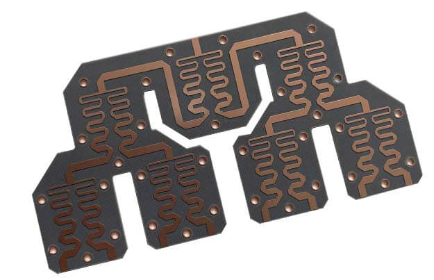
Releted High Speed PCB Products


Why Choose SMTFAB for Your High Speed PCB
In short, high-speed PCB design refers to any design where signal integrity begins to be affected by the physical characteristics of the circuit board, such as layout, packaging, layer stacking, interconnection, etc.. To delay, attenuation, crosstalk, reflection or emission, etc.
Congratulations! You have entered the world of high-speed PCB design.
As a reliable high speed PCB supplier, SMTFAB has one engineering team over 20 years design experience. We have served over 1000+ customers all around the world.
SMTFAB has many selections of high speed PCB design software, for example Altium Designer, Cadence Or CAD, Legacy PCAD, Eagle (Altium Conversion). Please tell us which software you need us to use in your project.
The reason why the high speed PCB design is so unique is the level of attention paid to these issues. You may be accustomed to designing simple circuit boards, where most of your time is spent on component placement and routing.
But for high speed PCB design, it is more important to accurately consider the placement of the trace, the width of the trace, the distance from other signals, and the type of connected components.
When you have to make such considerations, your high speed PCB design process will reach a whole new level.
Please send your quote to us right now, we will offer the quotation immediately.
High Speed PCB Background
AI, Autonomous driving, 5G, IoT and smart connectivity have increased the need for high data transfer rates and greater bandwidth which requires a multigenerational connectivity network over the next few decades.
The demands for high speed and high frequency PCB become more and more,meanwhile,the ubiquitous demand for data and connectivity has created needs for materials with unique properties to deliver high performance in this expanding ecosystem.
What is Copper Clad Laminate?
Copper clad laminate is also known as base material. The reinforcing material is impregnated with resin, one or both sides are covered with copper foil, and a plate-like material is formed by hot pressing, which is called copper clad laminate.
It is the basic material for PCB, often called substrate. When it is used for multilayer board production, it is also called core board (CORE)
High Speed PCB Copper Clad Laminate Process
The preparation process of high frequency copper clad laminate is similar to that of ordinary copper clad laminate:
- Glue mixing: The special resin, solvent, and filler are pumped into the glue mixing tank through a pipeline according to a certain proportion and stirred. The materials need to be stirred to prepare a viscous glue with fluidity.
- Gluing and drying: Pump the mixed glue into the glue tank, and at the same time, continuously immerse the glass fiber cloth into the glue tank through the glue machine to make the glue adhere to the glass fiber cloth. The glued glass fiber cloth enters the glue machine oven and is dried at high temperature to become a bonded sheet.
- BOOK after cutting the sticky slices: The dried sticky slices are trimmed as required, and the sticking slices (1 or more) and copper foil are stacked and transported to the clean room. Use an automatic BOOK machine to combine the prepared material and the steel plate.
- Laminating: Send the assembled semi-finished product from the automatic conveyor to the hot press machine, so that the product can be kept in a high temperature, high pressure and vacuum environment for several hours, thenthe bonding sheet and copper foil are connected together, and finally It becomes a finished copper clad laminate with surface copper foil and intermediate insulating layer.
- Shearing: After cooling, trim the extra side strips of the disassembled product, and cut it into corresponding size and according to customer requirements.
Introduction for 5G PCBs of High Frequency and High Speed PCB Materials
The CCL industry is in the middle of the entire PCB industry chain, providing raw materials for PCB products.
Copper-clad laminate is a plate-like material made by dipping, cutting and laminating electronic glass fiber cloth or other reinforcing materials into resin blanks, covering copper foil on one side or both sides and hot pressing.
It is mainly used to make printed circuit boards (PCB), which play the role of interconnection, insulation and support for PCB.
The upstream of the industrial chain is electrolytic copper foil, wood pulp paper, glass fiber cloth, resin and other raw materials, the downstream is PCB products, and the terminal industry is aerospace, automobiles, home appliances, communications, computers and so on.
In 2019, the initial commercial use of 5G. The upstream materials of core materials such as high-frequency copper clad laminates are basically similar to traditional CCL.
After being produced by downstream PCB manufacturers as high-frequency circuit boards suitable for high-frequency environments, they are used in base station antenna modules and power amplifiers.
Modules and other equipment components, and eventually widely used in high-frequency communication fields such as communication base stations (antennas, power amplifiers, low-noise amplifiers, filters, etc.), automotive auxiliary systems, aerospace technology, satellite communications, satellite TV, military radar, etc.
5G High Frequency Technology Places Higher Demands on High Speed PCBs.
Radio frequency circuits with operating frequencies above 1 GHz are generally called high-frequency circuits.
In the process of mobile communication from 2G to 3G and 4G, the communication frequency band has developed from 800 MHz to 2.5 GHz. In the 5G era, the communication frequency band will be further improved.
The PCB board will be equipped with antenna elements, filters and other devices in the 5G radio frequency.
According to the requirements of the Ministry of Industry and Information Technology, the early 5G deployment is expected to use the 3.5GHz frequency band, and the 4G frequency band is mainly around 2GHz.
Generally, electromagnetic waves with a wavelength of 1–10 mm in the 30–300 GHz frequency band are millimeter waves.
In 5G Large-Scale Commercial Use, Millimeter Wave Technology Ensures Better Performance:
The bandwidth is extremely wide, the available spectrum bandwidth of the 28GHz band can reach 1GHz, and the available signal bandwidth of each channel of the 60GHz band can reach 2GHz;
The corresponding antenna has high resolution and anti-interference performance Good, miniaturization can be achieved; the propagation attenuation in the atmosphere is faster, and close-range confidential communication can be achieved.
In order to solve the needs of high frequency and high speed, as well as to deal with the problems of poor millimeter wave penetration and fast attenuation, 5G communication equipment has the following three performance requirements for PCB:
- Low transmission loss;
- Low transmission delay;
- Precision control of high characteristic impedance.
There are two ways to increase the frequency of PCBs.
One is that the PCB manufacturing process requires more, and the other is to use high-frequency CCL-the substrate material that meets the high-frequency application environment is called high-frequency copper clad.
There are Mainly two Indicators of Dielectric Constant (Dk) and Dielectric Loss Factor (Df) to Measure the Performance of High Frequency Copper Clad Llaminate Materials.
The smaller the Dk and Df, the more stable, the better the performance of the high-frequency high-speed substrate.
In addition, for the RF board, the PCB board has a larger area and more layers, which requires the substrate to have higher heat resistance (Tg, high temperature modulus retention rate) and stricter thickness tolerances.
How to Design High Speed PCB?
In terms of high speed and high frequency circuits, high-frequency circuit boards made of high-dielectric and high-frequency substrates are very necessary.
To achieve good performance design, high-frequency circuit boards have their own details that need to be paid attention to.
Now I will explain about high-frequency circuit board design Of the eight details.
- Use high-performance dielectric circuit boards whose dielectric constant values are strictly controlled according to the number of layers. This method is conducive to effective simulation calculation of the electromagnetic field between the insulating material and the adjacent wiring.
- The corner of the transmission line should be 45° to reduce the return loss.
- The protruding pin leads have tap inductance and parasitic effects. Avoid using components with leads. In high frequency environments, it is best to use surface mount SMD components.
- To specify PCB design specifications related to high-precision etching. It is necessary to consider that the total error of the specified line width is +/-0.0007 inches, the undercut and cross section of the wiring shape should be managed, and the plating conditions of the wiring side wall should be specified. The overall management of wiring (wire) geometry and coating surface is very important to solve the skin effect problem related to microwave frequency and realize these specifications.
- As for signal vias, avoid using a via processing (PTH) process on sensitive boards, because this process will cause lead inductance at the via. For example, when a through hole on a 20-layer board is used to connect layers 1 to 3, there are lead inductance in between 4 to 19 layers, so buried /blind drills or back drills should be used.
- To choose electroless nickel plating or immersion gold plating process, do not use HASL method for electroplating. This kind of electroplated surface can provide better skin effect for high frequency current. In addition, this highly solderable coating requires fewer leads, which helps reduce environmental pollution. To provide a rich ground layer,use molded holes to connect these ground planes to prevent the 3D electromagnetic field from affecting the circuit board.
- To provide a rich ground plane. Use molded holes to connect these ground planes to prevent the 3D electromagnetic field from affecting the circuit board.
- The solder mask can prevent the flow of solder paste. However, due to the uncertainty of thickness and the unknown of dielectric constant performance, covering the entire board surface with solder mask material will cause changes in circuit performance in the microstrip design. Generally, a solder dam is used as the solder mask.
Your Valuable High Speed PCB Manufacturer in China
SMTFAB is a professional high speed PCB manufacturer in China. As 5G era is coming, high speed PCBs need more and more in different applications.
- Over 12 years high speed PCB manufacturing experience
- No minimum order quantity for high speed PCB order
- Complete PCB material in stock like Taconic, Rogers, Arlon
- 100% E-test and AOI inspection
- 24h quick turn service for your prototype of high speed PCB
- Production Facility
- Capabilities
Please Check SMTFAB High Frequency PCB Manufacturing Capabilities in the Following Table:
| Feature | Capability |
| Material | RO4003C, RO4350B, Ro3003, Ro3010, RT5880,Teflon |
| Min. Track/Spacing | 2mil |
| Min. Hole Size | 0.15mm |
| Finished Cooper | 1-2oz |
| Board Thickness | 0.2-3.2mm |
| Surface Finishing | Immersion gold, OSP, LF HAL,Hard Gold,Immersion Silver,Immersion Tin,Enepig |
| Finsih Cooper | 0.5-12oz |
| Solder Mask | Green, Red, Yellow, Blue, White, Black, Purple,Orange, Matte Black, Matte Green,Matte Blue |
| Silkscreen | White, Black |
| Via Process | Tenting Vias,Plugged Vias,Vias not covered |
| Testing | Fly Probe Testing (Free) and A.O.I. testing |
| Build time | 5-10 days |
| Lead time | 2-3 days |
Releted High Speed PCB Products
Why Choose SMTFAB for Your High Speed PCB
In short, high-speed PCB design refers to any design where signal integrity begins to be affected by the physical characteristics of the circuit board, such as layout, packaging, layer stacking, interconnection, etc.. To delay, attenuation, crosstalk, reflection or emission, etc.
Congratulations! You have entered the world of high-speed PCB design.
As a reliable high speed PCB supplier, SMTFAB has one engineering team over 20 years design experience. We have served over 1000+ customers all around the world.
SMTFAB has many selections of high speed PCB design software, for example Altium Designer, Cadence Or CAD, Legacy PCAD, Eagle (Altium Conversion). Please tell us which software you need us to use in your project.
The reason why the high speed PCB design is so unique is the level of attention paid to these issues. You may be accustomed to designing simple circuit boards, where most of your time is spent on component placement and routing.
But for high speed PCB design, it is more important to accurately consider the placement of the trace, the width of the trace, the distance from other signals, and the type of connected components.
When you have to make such considerations, your high speed PCB design process will reach a whole new level.
Please send your quote to us right now, we will offer the quotation immediately.
High Speed PCB Background
AI, Autonomous driving, 5G, IoT and smart connectivity have increased the need for high data transfer rates and greater bandwidth which requires a multigenerational connectivity network over the next few decades.
The demands for high speed and high frequency PCB become more and more,meanwhile,the ubiquitous demand for data and connectivity has created needs for materials with unique properties to deliver high performance in this expanding ecosystem.
What is Copper Clad Laminate?
Copper clad laminate is also known as base material. The reinforcing material is impregnated with resin, one or both sides are covered with copper foil, and a plate-like material is formed by hot pressing, which is called copper clad laminate.
It is the basic material for PCB, often called substrate. When it is used for multilayer board production, it is also called core board (CORE)
High Speed PCB Copper Clad Laminate Process
The preparation process of high frequency copper clad laminate is similar to that of ordinary copper clad laminate:
- Glue mixing: The special resin, solvent, and filler are pumped into the glue mixing tank through a pipeline according to a certain proportion and stirred. The materials need to be stirred to prepare a viscous glue with fluidity.
- Gluing and drying: Pump the mixed glue into the glue tank, and at the same time, continuously immerse the glass fiber cloth into the glue tank through the glue machine to make the glue adhere to the glass fiber cloth. The glued glass fiber cloth enters the glue machine oven and is dried at high temperature to become a bonded sheet.
- BOOK after cutting the sticky slices: The dried sticky slices are trimmed as required, and the sticking slices (1 or more) and copper foil are stacked and transported to the clean room. Use an automatic BOOK machine to combine the prepared material and the steel plate.
- Laminating: Send the assembled semi-finished product from the automatic conveyor to the hot press machine, so that the product can be kept in a high temperature, high pressure and vacuum environment for several hours, thenthe bonding sheet and copper foil are connected together, and finally It becomes a finished copper clad laminate with surface copper foil and intermediate insulating layer.
- Shearing: After cooling, trim the extra side strips of the disassembled product, and cut it into corresponding size and according to customer requirements.
Introduction for 5G PCBs of High Frequency and High Speed PCB Materials
The CCL industry is in the middle of the entire PCB industry chain, providing raw materials for PCB products.
Copper-clad laminate is a plate-like material made by dipping, cutting and laminating electronic glass fiber cloth or other reinforcing materials into resin blanks, covering copper foil on one side or both sides and hot pressing.
It is mainly used to make printed circuit boards (PCB), which play the role of interconnection, insulation and support for PCB.
The upstream of the industrial chain is electrolytic copper foil, wood pulp paper, glass fiber cloth, resin and other raw materials, the downstream is PCB products, and the terminal industry is aerospace, automobiles, home appliances, communications, computers and so on.
In 2019, the initial commercial use of 5G. The upstream materials of core materials such as high-frequency copper clad laminates are basically similar to traditional CCL.
After being produced by downstream PCB manufacturers as high-frequency circuit boards suitable for high-frequency environments, they are used in base station antenna modules and power amplifiers.
Modules and other equipment components, and eventually widely used in high-frequency communication fields such as communication base stations (antennas, power amplifiers, low-noise amplifiers, filters, etc.), automotive auxiliary systems, aerospace technology, satellite communications, satellite TV, military radar, etc.
5G High Frequency Technology Places Higher Demands on High Speed PCBs.
Radio frequency circuits with operating frequencies above 1 GHz are generally called high-frequency circuits.
In the process of mobile communication from 2G to 3G and 4G, the communication frequency band has developed from 800 MHz to 2.5 GHz. In the 5G era, the communication frequency band will be further improved.
The PCB board will be equipped with antenna elements, filters and other devices in the 5G radio frequency.
According to the requirements of the Ministry of Industry and Information Technology, the early 5G deployment is expected to use the 3.5GHz frequency band, and the 4G frequency band is mainly around 2GHz.
Generally, electromagnetic waves with a wavelength of 1–10 mm in the 30–300 GHz frequency band are millimeter waves.
In 5G Large-Scale Commercial Use, Millimeter Wave Technology Ensures Better Performance:
The bandwidth is extremely wide, the available spectrum bandwidth of the 28GHz band can reach 1GHz, and the available signal bandwidth of each channel of the 60GHz band can reach 2GHz;
The corresponding antenna has high resolution and anti-interference performance Good, miniaturization can be achieved; the propagation attenuation in the atmosphere is faster, and close-range confidential communication can be achieved.
In order to solve the needs of high frequency and high speed, as well as to deal with the problems of poor millimeter wave penetration and fast attenuation, 5G communication equipment has the following three performance requirements for PCB:
- Low transmission loss;
- Low transmission delay;
- Precision control of high characteristic impedance.
There are two ways to increase the frequency of PCBs.
One is that the PCB manufacturing process requires more, and the other is to use high-frequency CCL-the substrate material that meets the high-frequency application environment is called high-frequency copper clad.
There are Mainly two Indicators of Dielectric Constant (Dk) and Dielectric Loss Factor (Df) to Measure the Performance of High Frequency Copper Clad Llaminate Materials.
The smaller the Dk and Df, the more stable, the better the performance of the high-frequency high-speed substrate.
In addition, for the RF board, the PCB board has a larger area and more layers, which requires the substrate to have higher heat resistance (Tg, high temperature modulus retention rate) and stricter thickness tolerances.
How to Design High Speed PCB?
In terms of high speed and high frequency circuits, high-frequency circuit boards made of high-dielectric and high-frequency substrates are very necessary.
To achieve good performance design, high-frequency circuit boards have their own details that need to be paid attention to.
Now I will explain about high-frequency circuit board design Of the eight details.
- Use high-performance dielectric circuit boards whose dielectric constant values are strictly controlled according to the number of layers. This method is conducive to effective simulation calculation of the electromagnetic field between the insulating material and the adjacent wiring.
- The corner of the transmission line should be 45° to reduce the return loss.
- The protruding pin leads have tap inductance and parasitic effects. Avoid using components with leads. In high frequency environments, it is best to use surface mount SMD components.
- To specify PCB design specifications related to high-precision etching. It is necessary to consider that the total error of the specified line width is +/-0.0007 inches, the undercut and cross section of the wiring shape should be managed, and the plating conditions of the wiring side wall should be specified. The overall management of wiring (wire) geometry and coating surface is very important to solve the skin effect problem related to microwave frequency and realize these specifications.
- As for signal vias, avoid using a via processing (PTH) process on sensitive boards, because this process will cause lead inductance at the via. For example, when a through hole on a 20-layer board is used to connect layers 1 to 3, there are lead inductance in between 4 to 19 layers, so buried /blind drills or back drills should be used.
- To choose electroless nickel plating or immersion gold plating process, do not use HASL method for electroplating. This kind of electroplated surface can provide better skin effect for high frequency current. In addition, this highly solderable coating requires fewer leads, which helps reduce environmental pollution. To provide a rich ground layer,use molded holes to connect these ground planes to prevent the 3D electromagnetic field from affecting the circuit board.
- To provide a rich ground plane. Use molded holes to connect these ground planes to prevent the 3D electromagnetic field from affecting the circuit board.
- The solder mask can prevent the flow of solder paste. However, due to the uncertainty of thickness and the unknown of dielectric constant performance, covering the entire board surface with solder mask material will cause changes in circuit performance in the microstrip design. Generally, a solder dam is used as the solder mask.
Your Valuable High Speed PCB Manufacturer in China
SMTFAB is a professional high speed PCB manufacturer in China. As 5G era is coming, high speed PCBs need more and more in different applications.
- Over 12 years high speed PCB manufacturing experience
- No minimum order quantity for high speed PCB order
- Complete PCB material in stock like Taconic, Rogers, Arlon
- 100% E-test and AOI inspection
- 24h quick turn service for your prototype of high speed PCB
Your Valuable High Speed PCB Manufacturer in China
Your Valuable High Speed PCB Manufacturer in China
SMTFAB is a professional high speed PCB manufacturer in China. As 5G era is coming, high speed PCBs need more and more in different applications.
- Over 12 years high speed PCB manufacturing experience
- No minimum order quantity for high speed PCB order
- Complete PCB material in stock like Taconic, Rogers, Arlon
- 100% E-test and AOI inspection
- 24h quick turn service for your prototype of high speed PCB
- Production Facility
- Capabilities
Please Check SMTFAB High Frequency PCB Manufacturing Capabilities in the Following Table:
| Feature | Capability |
| Material | RO4003C, RO4350B, Ro3003, Ro3010, RT5880,Teflon |
| Min. Track/Spacing | 2mil |
| Min. Hole Size | 0.15mm |
| Finished Cooper | 1-2oz |
| Board Thickness | 0.2-3.2mm |
| Surface Finishing | Immersion gold, OSP, LF HAL,Hard Gold,Immersion Silver,Immersion Tin,Enepig |
| Finsih Cooper | 0.5-12oz |
| Solder Mask | Green, Red, Yellow, Blue, White, Black, Purple,Orange, Matte Black, Matte Green,Matte Blue |
| Silkscreen | White, Black |
| Via Process | Tenting Vias,Plugged Vias,Vias not covered |
| Testing | Fly Probe Testing (Free) and A.O.I. testing |
| Build time | 5-10 days |
| Lead time | 2-3 days |
Releted High Speed PCB Products
Releted High Speed PCB Products
Why Choose SMTFAB for Your High Speed PCB
In short, high-speed PCB design refers to any design where signal integrity begins to be affected by the physical characteristics of the circuit board, such as layout, packaging, layer stacking, interconnection, etc.. To delay, attenuation, crosstalk, reflection or emission, etc.
Congratulations! You have entered the world of high-speed PCB design.
As a reliable high speed PCB supplier, SMTFAB has one engineering team over 20 years design experience. We have served over 1000+ customers all around the world.
SMTFAB has many selections of high speed PCB design software, for example Altium Designer, Cadence Or CAD, Legacy PCAD, Eagle (Altium Conversion). Please tell us which software you need us to use in your project.
The reason why the high speed PCB design is so unique is the level of attention paid to these issues. You may be accustomed to designing simple circuit boards, where most of your time is spent on component placement and routing.
But for high speed PCB design, it is more important to accurately consider the placement of the trace, the width of the trace, the distance from other signals, and the type of connected components.
When you have to make such considerations, your high speed PCB design process will reach a whole new level.
Please send your quote to us right now, we will offer the quotation immediately.
High Speed PCB Background
AI, Autonomous driving, 5G, IoT and smart connectivity have increased the need for high data transfer rates and greater bandwidth which requires a multigenerational connectivity network over the next few decades.
The demands for high speed and high frequency PCB become more and more,meanwhile,the ubiquitous demand for data and connectivity has created needs for materials with unique properties to deliver high performance in this expanding ecosystem.
What is Copper Clad Laminate?
Copper clad laminate is also known as base material. The reinforcing material is impregnated with resin, one or both sides are covered with copper foil, and a plate-like material is formed by hot pressing, which is called copper clad laminate.
It is the basic material for PCB, often called substrate. When it is used for multilayer board production, it is also called core board (CORE)
High Speed PCB Copper Clad Laminate Process
The preparation process of high frequency copper clad laminate is similar to that of ordinary copper clad laminate:
- Glue mixing: The special resin, solvent, and filler are pumped into the glue mixing tank through a pipeline according to a certain proportion and stirred. The materials need to be stirred to prepare a viscous glue with fluidity.
- Gluing and drying: Pump the mixed glue into the glue tank, and at the same time, continuously immerse the glass fiber cloth into the glue tank through the glue machine to make the glue adhere to the glass fiber cloth. The glued glass fiber cloth enters the glue machine oven and is dried at high temperature to become a bonded sheet.
- BOOK after cutting the sticky slices: The dried sticky slices are trimmed as required, and the sticking slices (1 or more) and copper foil are stacked and transported to the clean room. Use an automatic BOOK machine to combine the prepared material and the steel plate.
- Laminating: Send the assembled semi-finished product from the automatic conveyor to the hot press machine, so that the product can be kept in a high temperature, high pressure and vacuum environment for several hours, thenthe bonding sheet and copper foil are connected together, and finally It becomes a finished copper clad laminate with surface copper foil and intermediate insulating layer.
- Shearing: After cooling, trim the extra side strips of the disassembled product, and cut it into corresponding size and according to customer requirements.
Introduction for 5G PCBs of High Frequency and High Speed PCB Materials
The CCL industry is in the middle of the entire PCB industry chain, providing raw materials for PCB products.
Copper-clad laminate is a plate-like material made by dipping, cutting and laminating electronic glass fiber cloth or other reinforcing materials into resin blanks, covering copper foil on one side or both sides and hot pressing.
It is mainly used to make printed circuit boards (PCB), which play the role of interconnection, insulation and support for PCB.
The upstream of the industrial chain is electrolytic copper foil, wood pulp paper, glass fiber cloth, resin and other raw materials, the downstream is PCB products, and the terminal industry is aerospace, automobiles, home appliances, communications, computers and so on.
In 2019, the initial commercial use of 5G. The upstream materials of core materials such as high-frequency copper clad laminates are basically similar to traditional CCL.
After being produced by downstream PCB manufacturers as high-frequency circuit boards suitable for high-frequency environments, they are used in base station antenna modules and power amplifiers.
Modules and other equipment components, and eventually widely used in high-frequency communication fields such as communication base stations (antennas, power amplifiers, low-noise amplifiers, filters, etc.), automotive auxiliary systems, aerospace technology, satellite communications, satellite TV, military radar, etc.
5G High Frequency Technology Places Higher Demands on High Speed PCBs.
Radio frequency circuits with operating frequencies above 1 GHz are generally called high-frequency circuits.
In the process of mobile communication from 2G to 3G and 4G, the communication frequency band has developed from 800 MHz to 2.5 GHz. In the 5G era, the communication frequency band will be further improved.
The PCB board will be equipped with antenna elements, filters and other devices in the 5G radio frequency.
According to the requirements of the Ministry of Industry and Information Technology, the early 5G deployment is expected to use the 3.5GHz frequency band, and the 4G frequency band is mainly around 2GHz.
Generally, electromagnetic waves with a wavelength of 1–10 mm in the 30–300 GHz frequency band are millimeter waves.
In 5G Large-Scale Commercial Use, Millimeter Wave Technology Ensures Better Performance:
The bandwidth is extremely wide, the available spectrum bandwidth of the 28GHz band can reach 1GHz, and the available signal bandwidth of each channel of the 60GHz band can reach 2GHz;
The corresponding antenna has high resolution and anti-interference performance Good, miniaturization can be achieved; the propagation attenuation in the atmosphere is faster, and close-range confidential communication can be achieved.
In order to solve the needs of high frequency and high speed, as well as to deal with the problems of poor millimeter wave penetration and fast attenuation, 5G communication equipment has the following three performance requirements for PCB:
- Low transmission loss;
- Low transmission delay;
- Precision control of high characteristic impedance.
There are two ways to increase the frequency of PCBs.
One is that the PCB manufacturing process requires more, and the other is to use high-frequency CCL-the substrate material that meets the high-frequency application environment is called high-frequency copper clad.
There are Mainly two Indicators of Dielectric Constant (Dk) and Dielectric Loss Factor (Df) to Measure the Performance of High Frequency Copper Clad Llaminate Materials.
The smaller the Dk and Df, the more stable, the better the performance of the high-frequency high-speed substrate.
In addition, for the RF board, the PCB board has a larger area and more layers, which requires the substrate to have higher heat resistance (Tg, high temperature modulus retention rate) and stricter thickness tolerances.
How to Design High Speed PCB?
In terms of high speed and high frequency circuits, high-frequency circuit boards made of high-dielectric and high-frequency substrates are very necessary.
To achieve good performance design, high-frequency circuit boards have their own details that need to be paid attention to.
Now I will explain about high-frequency circuit board design Of the eight details.
- Use high-performance dielectric circuit boards whose dielectric constant values are strictly controlled according to the number of layers. This method is conducive to effective simulation calculation of the electromagnetic field between the insulating material and the adjacent wiring.
- The corner of the transmission line should be 45° to reduce the return loss.
- The protruding pin leads have tap inductance and parasitic effects. Avoid using components with leads. In high frequency environments, it is best to use surface mount SMD components.
- To specify PCB design specifications related to high-precision etching. It is necessary to consider that the total error of the specified line width is +/-0.0007 inches, the undercut and cross section of the wiring shape should be managed, and the plating conditions of the wiring side wall should be specified. The overall management of wiring (wire) geometry and coating surface is very important to solve the skin effect problem related to microwave frequency and realize these specifications.
- As for signal vias, avoid using a via processing (PTH) process on sensitive boards, because this process will cause lead inductance at the via. For example, when a through hole on a 20-layer board is used to connect layers 1 to 3, there are lead inductance in between 4 to 19 layers, so buried /blind drills or back drills should be used.
- To choose electroless nickel plating or immersion gold plating process, do not use HASL method for electroplating. This kind of electroplated surface can provide better skin effect for high frequency current. In addition, this highly solderable coating requires fewer leads, which helps reduce environmental pollution. To provide a rich ground layer,use molded holes to connect these ground planes to prevent the 3D electromagnetic field from affecting the circuit board.
- To provide a rich ground plane. Use molded holes to connect these ground planes to prevent the 3D electromagnetic field from affecting the circuit board.
- The solder mask can prevent the flow of solder paste. However, due to the uncertainty of thickness and the unknown of dielectric constant performance, covering the entire board surface with solder mask material will cause changes in circuit performance in the microstrip design. Generally, a solder dam is used as the solder mask.
Why Choose SMTFAB for Your High Speed PCB
In short, high-speed PCB design refers to any design where signal integrity begins to be affected by the physical characteristics of the circuit board, such as layout, packaging, layer stacking, interconnection, etc.. To delay, attenuation, crosstalk, reflection or emission, etc.
Congratulations! You have entered the world of high-speed PCB design.
As a reliable high speed PCB supplier, SMTFAB has one engineering team over 20 years design experience. We have served over 1000+ customers all around the world.
SMTFAB has many selections of high speed PCB design software, for example Altium Designer, Cadence Or CAD, Legacy PCAD, Eagle (Altium Conversion). Please tell us which software you need us to use in your project.
The reason why the high speed PCB design is so unique is the level of attention paid to these issues. You may be accustomed to designing simple circuit boards, where most of your time is spent on component placement and routing.
But for high speed PCB design, it is more important to accurately consider the placement of the trace, the width of the trace, the distance from other signals, and the type of connected components.
When you have to make such considerations, your high speed PCB design process will reach a whole new level.
Please send your quote to us right now, we will offer the quotation immediately.
High Speed PCB Background
AI, Autonomous driving, 5G, IoT and smart connectivity have increased the need for high data transfer rates and greater bandwidth which requires a multigenerational connectivity network over the next few decades.
The demands for high speed and high frequency PCB become more and more,meanwhile,the ubiquitous demand for data and connectivity has created needs for materials with unique properties to deliver high performance in this expanding ecosystem.
- What is Copper Clad Laminate?
- High Speed PCB Copper Clad Laminate Process
- Introduction for 5G PCBs of High Frequency and High Speed PCB Materials
- 5G High Frequency Technology Places Higher Demands on High Speed PCBs.
- How to Design High Speed PCB?
What is Copper Clad Laminate?
Copper clad laminate is also known as base material. The reinforcing material is impregnated with resin, one or both sides are covered with copper foil, and a plate-like material is formed by hot pressing, which is called copper clad laminate.
It is the basic material for PCB, often called substrate. When it is used for multilayer board production, it is also called core board (CORE)
High Speed PCB Copper Clad Laminate Process
The preparation process of high frequency copper clad laminate is similar to that of ordinary copper clad laminate:
- Glue mixing: The special resin, solvent, and filler are pumped into the glue mixing tank through a pipeline according to a certain proportion and stirred. The materials need to be stirred to prepare a viscous glue with fluidity.
- Gluing and drying: Pump the mixed glue into the glue tank, and at the same time, continuously immerse the glass fiber cloth into the glue tank through the glue machine to make the glue adhere to the glass fiber cloth. The glued glass fiber cloth enters the glue machine oven and is dried at high temperature to become a bonded sheet.
- BOOK after cutting the sticky slices: The dried sticky slices are trimmed as required, and the sticking slices (1 or more) and copper foil are stacked and transported to the clean room. Use an automatic BOOK machine to combine the prepared material and the steel plate.
- Laminating: Send the assembled semi-finished product from the automatic conveyor to the hot press machine, so that the product can be kept in a high temperature, high pressure and vacuum environment for several hours, thenthe bonding sheet and copper foil are connected together, and finally It becomes a finished copper clad laminate with surface copper foil and intermediate insulating layer.
- Shearing: After cooling, trim the extra side strips of the disassembled product, and cut it into corresponding size and according to customer requirements.
Introduction for 5G PCBs of High Frequency and High Speed PCB Materials
The CCL industry is in the middle of the entire PCB industry chain, providing raw materials for PCB products.
Copper-clad laminate is a plate-like material made by dipping, cutting and laminating electronic glass fiber cloth or other reinforcing materials into resin blanks, covering copper foil on one side or both sides and hot pressing.
It is mainly used to make printed circuit boards (PCB), which play the role of interconnection, insulation and support for PCB.
The upstream of the industrial chain is electrolytic copper foil, wood pulp paper, glass fiber cloth, resin and other raw materials, the downstream is PCB products, and the terminal industry is aerospace, automobiles, home appliances, communications, computers and so on.
In 2019, the initial commercial use of 5G. The upstream materials of core materials such as high-frequency copper clad laminates are basically similar to traditional CCL.
After being produced by downstream PCB manufacturers as high-frequency circuit boards suitable for high-frequency environments, they are used in base station antenna modules and power amplifiers.
Modules and other equipment components, and eventually widely used in high-frequency communication fields such as communication base stations (antennas, power amplifiers, low-noise amplifiers, filters, etc.), automotive auxiliary systems, aerospace technology, satellite communications, satellite TV, military radar, etc.
5G High Frequency Technology Places Higher Demands on High Speed PCBs.
Radio frequency circuits with operating frequencies above 1 GHz are generally called high-frequency circuits.
In the process of mobile communication from 2G to 3G and 4G, the communication frequency band has developed from 800 MHz to 2.5 GHz. In the 5G era, the communication frequency band will be further improved.
The PCB board will be equipped with antenna elements, filters and other devices in the 5G radio frequency.
According to the requirements of the Ministry of Industry and Information Technology, the early 5G deployment is expected to use the 3.5GHz frequency band, and the 4G frequency band is mainly around 2GHz.
Generally, electromagnetic waves with a wavelength of 1–10 mm in the 30–300 GHz frequency band are millimeter waves.
In 5G Large-Scale Commercial Use, Millimeter Wave Technology Ensures Better Performance:
The bandwidth is extremely wide, the available spectrum bandwidth of the 28GHz band can reach 1GHz, and the available signal bandwidth of each channel of the 60GHz band can reach 2GHz;
The corresponding antenna has high resolution and anti-interference performance Good, miniaturization can be achieved; the propagation attenuation in the atmosphere is faster, and close-range confidential communication can be achieved.
In order to solve the needs of high frequency and high speed, as well as to deal with the problems of poor millimeter wave penetration and fast attenuation, 5G communication equipment has the following three performance requirements for PCB:
- Low transmission loss;
- Low transmission delay;
- Precision control of high characteristic impedance.
There are two ways to increase the frequency of PCBs.
One is that the PCB manufacturing process requires more, and the other is to use high-frequency CCL-the substrate material that meets the high-frequency application environment is called high-frequency copper clad.
There are Mainly two Indicators of Dielectric Constant (Dk) and Dielectric Loss Factor (Df) to Measure the Performance of High Frequency Copper Clad Llaminate Materials.
The smaller the Dk and Df, the more stable, the better the performance of the high-frequency high-speed substrate.
In addition, for the RF board, the PCB board has a larger area and more layers, which requires the substrate to have higher heat resistance (Tg, high temperature modulus retention rate) and stricter thickness tolerances.
How to Design High Speed PCB?
In terms of high speed and high frequency circuits, high-frequency circuit boards made of high-dielectric and high-frequency substrates are very necessary.
To achieve good performance design, high-frequency circuit boards have their own details that need to be paid attention to.
Now I will explain about high-frequency circuit board design Of the eight details.
- Use high-performance dielectric circuit boards whose dielectric constant values are strictly controlled according to the number of layers. This method is conducive to effective simulation calculation of the electromagnetic field between the insulating material and the adjacent wiring.
- The corner of the transmission line should be 45° to reduce the return loss.
- The protruding pin leads have tap inductance and parasitic effects. Avoid using components with leads. In high frequency environments, it is best to use surface mount SMD components.
- To specify PCB design specifications related to high-precision etching. It is necessary to consider that the total error of the specified line width is +/-0.0007 inches, the undercut and cross section of the wiring shape should be managed, and the plating conditions of the wiring side wall should be specified. The overall management of wiring (wire) geometry and coating surface is very important to solve the skin effect problem related to microwave frequency and realize these specifications.
- As for signal vias, avoid using a via processing (PTH) process on sensitive boards, because this process will cause lead inductance at the via. For example, when a through hole on a 20-layer board is used to connect layers 1 to 3, there are lead inductance in between 4 to 19 layers, so buried /blind drills or back drills should be used.
- To choose electroless nickel plating or immersion gold plating process, do not use HASL method for electroplating. This kind of electroplated surface can provide better skin effect for high frequency current. In addition, this highly solderable coating requires fewer leads, which helps reduce environmental pollution. To provide a rich ground layer,use molded holes to connect these ground planes to prevent the 3D electromagnetic field from affecting the circuit board.
- To provide a rich ground plane. Use molded holes to connect these ground planes to prevent the 3D electromagnetic field from affecting the circuit board.
- The solder mask can prevent the flow of solder paste. However, due to the uncertainty of thickness and the unknown of dielectric constant performance, covering the entire board surface with solder mask material will cause changes in circuit performance in the microstrip design. Generally, a solder dam is used as the solder mask.
Technical Specifications
| 0 | { |
| 1 | " |
| 2 | F |
| 3 | e |
| 4 | a |
| 5 | t |
| 6 | u |
| 7 | r |
| 8 | e |
| 9 | " |
| 10 | : |
| 11 | " |
| 12 | C |
| 13 | a |
| 14 | p |
| 15 | a |
| 16 | b |
| 17 | i |
| 18 | l |
| 19 | i |
| 20 | t |
| 21 | y |
| 22 | " |
| 23 | , |
| 24 | " |
| 25 | M |
| 26 | a |
| 27 | t |
| 28 | e |
| 29 | r |
| 30 | i |
| 31 | a |
| 32 | l |
| 33 | " |
| 34 | : |
| 35 | " |
| 36 | R |
| 37 | O |
| 38 | 4 |
| 39 | 0 |
| 40 | 0 |
| 41 | 3 |
| 42 | C |
| 43 | , |
| 44 | |
| 45 | R |
| 46 | O |
| 47 | 4 |
| 48 | 3 |
| 49 | 5 |
| 50 | 0 |
| 51 | B |
| 52 | , |
| 53 | |
| 54 | R |
| 55 | o |
| 56 | 3 |
| 57 | 0 |
| 58 | 0 |
| 59 | 3 |
| 60 | , |
| 61 | |
| 62 | R |
| 63 | o |
| 64 | 3 |
| 65 | 0 |
| 66 | 1 |
| 67 | 0 |
| 68 | , |
| 69 | |
| 70 | R |
| 71 | T |
| 72 | 5 |
| 73 | 8 |
| 74 | 8 |
| 75 | 0 |
| 76 | , |
| 77 | T |
| 78 | e |
| 79 | f |
| 80 | l |
| 81 | o |
| 82 | n |
| 83 | " |
| 84 | , |
| 85 | " |
| 86 | M |
| 87 | i |
| 88 | n |
| 89 | . |
| 90 | |
| 91 | T |
| 92 | r |
| 93 | a |
| 94 | c |
| 95 | k |
| 96 | / |
| 97 | S |
| 98 | p |
| 99 | a |
| 100 | c |
| 101 | i |
| 102 | n |
| 103 | g |
| 104 | " |
| 105 | : |
| 106 | " |
| 107 | 2 |
| 108 | m |
| 109 | i |
| 110 | l |
| 111 | " |
| 112 | , |
| 113 | " |
| 114 | M |
| 115 | i |
| 116 | n |
| 117 | . |
| 118 | |
| 119 | H |
| 120 | o |
| 121 | l |
| 122 | e |
| 123 | |
| 124 | S |
| 125 | i |
| 126 | z |
| 127 | e |
| 128 | " |
| 129 | : |
| 130 | " |
| 131 | 0 |
| 132 | . |
| 133 | 1 |
| 134 | 5 |
| 135 | m |
| 136 | m |
| 137 | " |
| 138 | , |
| 139 | " |
| 140 | F |
| 141 | i |
| 142 | n |
| 143 | i |
| 144 | s |
| 145 | h |
| 146 | e |
| 147 | d |
| 148 | |
| 149 | C |
| 150 | o |
| 151 | o |
| 152 | p |
| 153 | e |
| 154 | r |
| 155 | " |
| 156 | : |
| 157 | " |
| 158 | 1 |
| 159 | - |
| 160 | 2 |
| 161 | o |
| 162 | z |
| 163 | " |
| 164 | , |
| 165 | " |
| 166 | B |
| 167 | o |
| 168 | a |
| 169 | r |
| 170 | d |
| 171 | |
| 172 | T |
| 173 | h |
| 174 | i |
| 175 | c |
| 176 | k |
| 177 | n |
| 178 | e |
| 179 | s |
| 180 | s |
| 181 | " |
| 182 | : |
| 183 | " |
| 184 | 0 |
| 185 | . |
| 186 | 2 |
| 187 | - |
| 188 | 3 |
| 189 | . |
| 190 | 2 |
| 191 | m |
| 192 | m |
| 193 | " |
| 194 | , |
| 195 | " |
| 196 | S |
| 197 | u |
| 198 | r |
| 199 | f |
| 200 | a |
| 201 | c |
| 202 | e |
| 203 | |
| 204 | F |
| 205 | i |
| 206 | n |
| 207 | i |
| 208 | s |
| 209 | h |
| 210 | i |
| 211 | n |
| 212 | g |
| 213 | " |
| 214 | : |
| 215 | " |
| 216 | I |
| 217 | m |
| 218 | m |
| 219 | e |
| 220 | r |
| 221 | s |
| 222 | i |
| 223 | o |
| 224 | n |
| 225 | |
| 226 | g |
| 227 | o |
| 228 | l |
| 229 | d |
| 230 | , |
| 231 | |
| 232 | O |
| 233 | S |
| 234 | P |
| 235 | , |
| 236 | |
| 237 | L |
| 238 | F |
| 239 | |
| 240 | H |
| 241 | A |
| 242 | L |
| 243 | , |
| 244 | H |
| 245 | a |
| 246 | r |
| 247 | d |
| 248 | |
| 249 | G |
| 250 | o |
| 251 | l |
| 252 | d |
| 253 | , |
| 254 | I |
| 255 | m |
| 256 | m |
| 257 | e |
| 258 | r |
| 259 | s |
| 260 | i |
| 261 | o |
| 262 | n |
| 263 | |
| 264 | S |
| 265 | i |
| 266 | l |
| 267 | v |
| 268 | e |
| 269 | r |
| 270 | , |
| 271 | I |
| 272 | m |
| 273 | m |
| 274 | e |
| 275 | r |
| 276 | s |
| 277 | i |
| 278 | o |
| 279 | n |
| 280 | |
| 281 | T |
| 282 | i |
| 283 | n |
| 284 | , |
| 285 | E |
| 286 | n |
| 287 | e |
| 288 | p |
| 289 | i |
| 290 | g |
| 291 | " |
| 292 | , |
| 293 | " |
| 294 | F |
| 295 | i |
| 296 | n |
| 297 | s |
| 298 | i |
| 299 | h |
| 300 | |
| 301 | C |
| 302 | o |
| 303 | o |
| 304 | p |
| 305 | e |
| 306 | r |
| 307 | " |
| 308 | : |
| 309 | " |
| 310 | 0 |
| 311 | . |
| 312 | 5 |
| 313 | - |
| 314 | 1 |
| 315 | 2 |
| 316 | o |
| 317 | z |
| 318 | " |
| 319 | , |
| 320 | " |
| 321 | S |
| 322 | o |
| 323 | l |
| 324 | d |
| 325 | e |
| 326 | r |
| 327 | |
| 328 | M |
| 329 | a |
| 330 | s |
| 331 | k |
| 332 | " |
| 333 | : |
| 334 | " |
| 335 | G |
| 336 | r |
| 337 | e |
| 338 | e |
| 339 | n |
| 340 | , |
| 341 | |
| 342 | R |
| 343 | e |
| 344 | d |
| 345 | , |
| 346 | |
| 347 | Y |
| 348 | e |
| 349 | l |
| 350 | l |
| 351 | o |
| 352 | w |
| 353 | , |
| 354 | |
| 355 | B |
| 356 | l |
| 357 | u |
| 358 | e |
| 359 | , |
| 360 | |
| 361 | W |
| 362 | h |
| 363 | i |
| 364 | t |
| 365 | e |
| 366 | , |
| 367 | |
| 368 | B |
| 369 | l |
| 370 | a |
| 371 | c |
| 372 | k |
| 373 | , |
| 374 | |
| 375 | P |
| 376 | u |
| 377 | r |
| 378 | p |
| 379 | l |
| 380 | e |
| 381 | , |
| 382 | O |
| 383 | r |
| 384 | a |
| 385 | n |
| 386 | g |
| 387 | e |
| 388 | , |
| 389 | |
| 390 | M |
| 391 | a |
| 392 | t |
| 393 | t |
| 394 | e |
| 395 | |
| 396 | B |
| 397 | l |
| 398 | a |
| 399 | c |
| 400 | k |
| 401 | , |
| 402 | |
| 403 | M |
| 404 | a |
| 405 | t |
| 406 | t |
| 407 | e |
| 408 | |
| 409 | G |
| 410 | r |
| 411 | e |
| 412 | e |
| 413 | n |
| 414 | , |
| 415 | M |
| 416 | a |
| 417 | t |
| 418 | t |
| 419 | e |
| 420 | |
| 421 | B |
| 422 | l |
| 423 | u |
| 424 | e |
| 425 | " |
| 426 | , |
| 427 | " |
| 428 | S |
| 429 | i |
| 430 | l |
| 431 | k |
| 432 | s |
| 433 | c |
| 434 | r |
| 435 | e |
| 436 | e |
| 437 | n |
| 438 | " |
| 439 | : |
| 440 | " |
| 441 | W |
| 442 | h |
| 443 | i |
| 444 | t |
| 445 | e |
| 446 | , |
| 447 | |
| 448 | B |
| 449 | l |
| 450 | a |
| 451 | c |
| 452 | k |
| 453 | " |
| 454 | , |
| 455 | " |
| 456 | V |
| 457 | i |
| 458 | a |
| 459 | |
| 460 | P |
| 461 | r |
| 462 | o |
| 463 | c |
| 464 | e |
| 465 | s |
| 466 | s |
| 467 | " |
| 468 | : |
| 469 | " |
| 470 | T |
| 471 | e |
| 472 | n |
| 473 | t |
| 474 | i |
| 475 | n |
| 476 | g |
| 477 | |
| 478 | V |
| 479 | i |
| 480 | a |
| 481 | s |
| 482 | , |
| 483 | P |
| 484 | l |
| 485 | u |
| 486 | g |
| 487 | g |
| 488 | e |
| 489 | d |
| 490 | |
| 491 | V |
| 492 | i |
| 493 | a |
| 494 | s |
| 495 | , |
| 496 | V |
| 497 | i |
| 498 | a |
| 499 | s |
| 500 | |
| 501 | n |
| 502 | o |
| 503 | t |
| 504 | |
| 505 | c |
| 506 | o |
| 507 | v |
| 508 | e |
| 509 | r |
| 510 | e |
| 511 | d |
| 512 | " |
| 513 | , |
| 514 | " |
| 515 | T |
| 516 | e |
| 517 | s |
| 518 | t |
| 519 | i |
| 520 | n |
| 521 | g |
| 522 | " |
| 523 | : |
| 524 | " |
| 525 | F |
| 526 | l |
| 527 | y |
| 528 | |
| 529 | P |
| 530 | r |
| 531 | o |
| 532 | b |
| 533 | e |
| 534 | |
| 535 | T |
| 536 | e |
| 537 | s |
| 538 | t |
| 539 | i |
| 540 | n |
| 541 | g |
| 542 | |
| 543 | ( |
| 544 | F |
| 545 | r |
| 546 | e |
| 547 | e |
| 548 | ) |
| 549 | |
| 550 | a |
| 551 | n |
| 552 | d |
| 553 | |
| 554 | A |
| 555 | . |
| 556 | O |
| 557 | . |
| 558 | I |
| 559 | . |
| 560 | |
| 561 | t |
| 562 | e |
| 563 | s |
| 564 | t |
| 565 | i |
| 566 | n |
| 567 | g |
| 568 | " |
| 569 | , |
| 570 | " |
| 571 | B |
| 572 | u |
| 573 | i |
| 574 | l |
| 575 | d |
| 576 | |
| 577 | t |
| 578 | i |
| 579 | m |
| 580 | e |
| 581 | " |
| 582 | : |
| 583 | " |
| 584 | 5 |
| 585 | - |
| 586 | 1 |
| 587 | 0 |
| 588 | |
| 589 | d |
| 590 | a |
| 591 | y |
| 592 | s |
| 593 | " |
| 594 | , |
| 595 | " |
| 596 | L |
| 597 | e |
| 598 | a |
| 599 | d |
| 600 | |
| 601 | t |
| 602 | i |
| 603 | m |
| 604 | e |
| 605 | " |
| 606 | : |
| 607 | " |
| 608 | 2 |
| 609 | - |
| 610 | 3 |
| 611 | |
| 612 | d |
| 613 | a |
| 614 | y |
| 615 | s |
| 616 | " |
| 617 | } |
Ready to Get Started?
Contact us today for a custom quote and expert consultation