Common PCB Design Mistakes and How to Avoid Them

Introduction
PCB design mistakes can result in manufacturing delays, increased costs, and product failures. Understanding common pitfalls helps you create better designs from the start.
1. Inadequate Clearances
Insufficient spacing between traces, pads, and components can cause manufacturing defects or electrical shorts. Always adhere to your manufacturer's minimum clearance requirements.
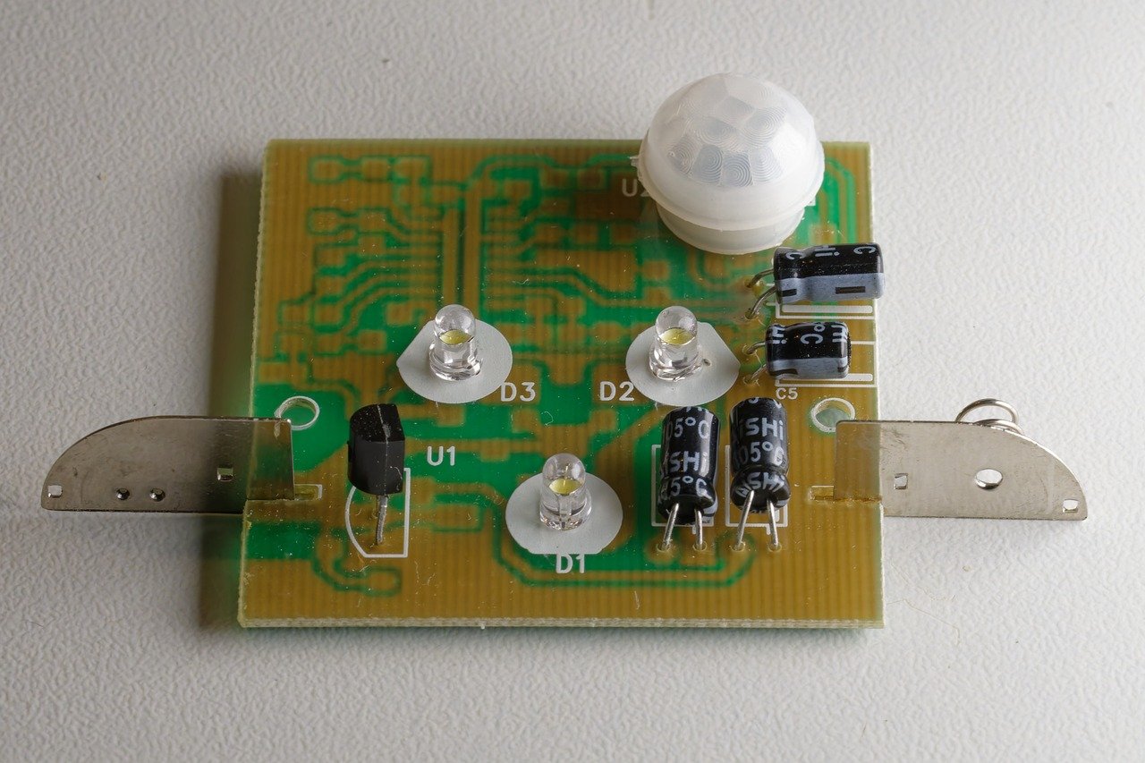
2. Poor Component Placement
Random component placement leads to longer traces, increased noise, and manufacturing difficulties. Plan your layout before placing components.
3. Missing or Incorrect Footprints
Using wrong component footprints is a costly mistake. Always verify footprints against manufacturer specifications and create custom footprints when needed.
4. Ignoring Thermal Considerations
Failing to account for heat dissipation can lead to component failure. Add thermal reliefs, heat sinks, and adequate copper pour for power components.
5. Inadequate Power Distribution
Undersized power traces or poor power plane design can cause voltage drops and system instability. Calculate power requirements and design accordingly.
6. No Design Rule Checks
Skipping DRC before manufacturing is risky. Always run comprehensive design rule checks and resolve all violations.
7. Poor Grounding Strategy
Inadequate grounding causes noise and EMI issues. Implement proper ground planes and star grounding where appropriate.
8. Missing Silkscreen Information
Insufficient labeling makes assembly and debugging difficult. Include clear reference designators, polarity marks, and component values.
Conclusion
Avoiding these common mistakes will significantly improve your PCB design quality and reduce time-to-market. Learn from others' experiences and always review your designs thoroughly.
Partagez cet article
Send Your Inquiry Today
We'll respond to your inquiry within 24 hours